A Novel Charge-Pumping Method for
Extracting the Lateral Distributions of
Interface-Trap and Effective Oxide-Trapped
Charge Densities in MOSFET Devices
Hsin-Hsien Li,
Student Member, IEEE,Yu-Lin Chu,
Student Member, IEEE,and Ching-Yuan Wu,
Member, IEEEAbstract— A novel charge-pumping method using dc source/
drain biases and specified gate waveforms is proposed to extract the lateral distributions of interface-trap and effective oxide-trapped charge densities. The surface potential redistribution due to the oxide-trapped charges is treated by an iteration process in order to accurately determine their lateral distributions. The proposed novel method is feasible for accurately extracting the distributions of interface-trap and effective oxide-trapped charge densities generated by the hot-carrier stress and can be further used to predict the device lifetime.
NOMENCLATURE
Flatband voltage.
High (low) voltage of the gate pulses. Time of the high (low) gate bias per cycle. Effective channel length.
Threshold voltage.
Surface electron (hole) concentration. Thermal velocity.
Hole (Electron) capture cross section. Intrinsic Fermi energy.
Intrinsic carrier concentration.
(Average) Interface-trap density per unit en-ergy.
Effective oxide trapped charge density. Trap energy level.
Elementary charge. Effective channel width. Frequency of gate pulses.
Lateral position along the channel. (Maximum) Charge pumping current. (Maximum) Recombined charge density per cycle.
Absolute slope of the rise (fall) edges of the gate pulses.
Boltzmann constant. Absolute temperature.
Manuscript received May 2, 1996; revised September 10, 1996. The review of this paper was arranged by Editor K. Tada. This work was supported by the National Science Council, Taiwan, R.O.C., under Contract NSC85-2215-E009-041.
The authors are with the Advanced Semiconductor Device Research Labo-ratory and Institute of Electronics, National Chiao-Tung University, Hsinchu 300, Taiwan, R.O.C.
Publisher Item Identifier S 0018-9383(97)03000-1.
Non-steady-state electron (hole) emission time.
Drain (source) current. Substrate voltage.
Drain-to-source (Source-to-drain) voltage. I. INTRODUCTION
W
ITH THE continuing scaling of MOS devices, the hot-carrier-induced device degradation has become a major reliability concern in sub- and deep-submicronmeter MOS-FET’s. It is believed that the degradation is mainly due to the effects of the generated oxide-trapped charges and interface-traps at the Si-SiO interface. In general, the large electric field is strongly localized near the drain, therefore, carrier injection and interface-trap creation are similarly concentrated. The strongly inharmonious characters of hot-carrier injection and resulted damages present a considerable challenge to both experimental and modeling efforts.One well-known experimental approach for measuring the Si-SiO interface-traps created by the hot-carrier stress is the charge-pumping technique [1]–[11]. In 1988, the ac drain pulse technique had been proposed to measure the spatial variations of hot-carrier-induced interface-trap density near the drain from small-geometry MOSFET’s [12]. After then, a similar technique had been developed to measure the lateral distribution of effective oxide-trapped charges [13]. However, according to our recent research [14], it is shown that the physical basis of using the ac source/drain pulses is incor-rect and the charge-pumping current is shown to be not sensitive to surface electric field in the inversion region but only sensitive to surface carrier concentration. Moreover, the extracted results using the ac source/drain method are sensitive to the applied waveforms and the delay time between the gate and source/drain pulses. Recently, a simple method has been proposed to derive the spatial distribution of hot-carrier induced interface-trap density [15], however, this method can only be applied for the case without oxide-trapped charges; moreover, its accuracy is poor.
In this paper, a novel charge-pumping method using dc source/drain biases is proposed to extract the lateral dis-tributions of both interface-trap and effective oxide-trapped charge densities. Based on the proposed new method, we can
LI et al.: NOVEL CHARGE-PUMPING METHOD 783
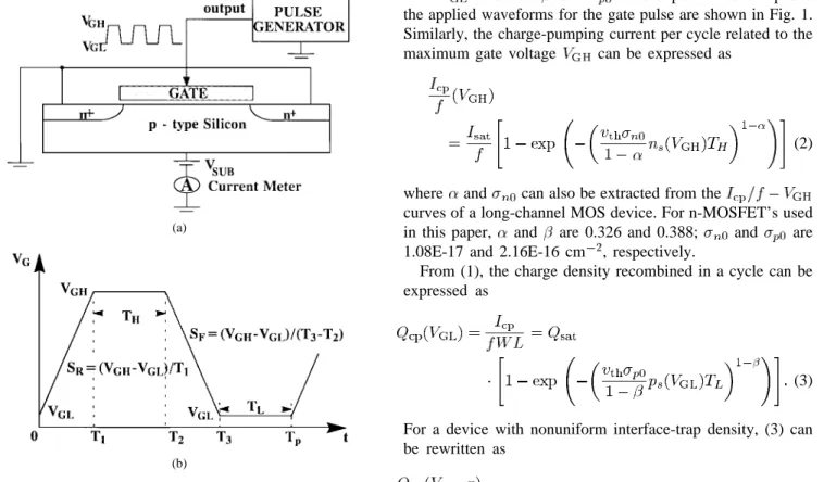
(a)
(b)
Fig. 1. (a) The experimental setup and (b) the applied gate pulse waveform for charge-pumping current measurement.
obtain the same damage profiles from the measured data under different gate or substrate biases. A detailed description of the proposed new method is given in Section I, which includes model derivations, applied gate waveform for measurements, and iteration process to obtain the accurate interface-trap density distribution. In Section II, the experimental results are presented, in which both the spatial damage distributions along the channel direction and the energy distribution of the interface traps in the bandgap have been extracted. In the last section, conclusions are made.
II. MODELDERIVATIONS ANDEXTRACTION METHOD
Based on a new charge-pumping current model [14] for a long-channel n-MOSFET with uniform interface-trap density distribution, the charge-pumping current per cycle related to the minimum gate voltage can be expressed as
(1) where is the saturation charge pumping current when the silicon surface is strongly inverted at , which is the func-tion of , and and can be obtained easily from the curves of a long-channel MOS device [14]; the value can be obtained from two-dimensional (2-D) numerical analysis. Note that the waveform used is important to obtain the correct results, the , and values are kept constant and the period is varied
with to obtain and The experimental setup and the applied waveforms for the gate pulse are shown in Fig. 1. Similarly, the charge-pumping current per cycle related to the maximum gate voltage can be expressed as
(2) where and can also be extracted from the
curves of a long-channel MOS device. For n-MOSFET’s used in this paper, and are 0.326 and 0.388; and are 1.08E-17 and 2.16E-16 cm , respectively.
From (1), the charge density recombined in a cycle can be expressed as
(3) For a device with nonuniform interface-trap density, (3) can be rewritten as
(4) where is the position along the channel direction, and
can be approximately expressed as
(5) with
(6) and
(7) Note that is the average interface-trap density from to is the nonsteady-state hole(electron) emission time [5]. For simplicity, at the proximity of the source/drain junction is assumed to be only related to the interface-trap density, i.e., and are independent of and and can be separately approximated as
(8) and
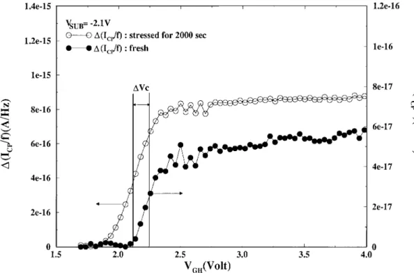
Fig. 2. The determination of 1Vc induced by the hot-carrier stress.
From (8) and (9), it is clear that is a function of through The total charge-pumping current per cycle for a device can be written as
(10) where
(11) If the silicon surface is accumulated at is equal to 1 in the middle of the channel and decreases to 0 rapidly at somewhere near the source/drain junction. The principal concept for obtaining the local interface-trap density is to measure the charge-pumping current contributed by a local area. In the previous methods [12], [13], the difference of the charge-pumping current measured with different substrate biases is used to extract the local interface-trap density. How-ever, because changes with , it becomes difficult to obtain accurately the charge-pumping current difference contributed completely by a local area. Using (8)–(9), it is obvious that if we keep , and unchanged, then
(10) can be expressed as
(12) and the charge pumping current difference per cycle measured from two low gate voltages and can be written as
(13) If the device is symmetrical, (13) can be rewritten as
(14) where is located at the center of the channel. If and are low enough to have the accumulated silicon surface, will be a highly localized weighting function near the junction, then we can obtain (15), shown at the bottom of the page, where
LI et al.: NOVEL CHARGE-PUMPING METHOD 785
Fig. 3. A flowchart showing the extraction process.
(16)
Note that used to measure should be high enough to strongly invert the silicon surface. Calculating at and using a 2-D device simulator, we can obtain interface-trap density distribution using (15).
If there is no long-channel device to extract the parameters and , an alternative method can be used. Using the “effective area” approach [16], we have
if
if (17)
TABLE I
DEVICEPARAMETERS OF THEn-MOSFET USED INTHISPAPER
where can be obtained from two MOSFET’s with different channel lengths. Using (17), (15) can be rewritten as
(18) where and can be obtained from
and However, the accuracy of (18) becomes poor when the interface-trap density is a fast changing function along the channel direction. Note that (15) and (18) can be used to calculate the interface-trap density of the unstressed devices. For the hot-carrier-stressed devices, one should measure the charge-pumping current before and after stress. Assuming the hot-carrier-induced damages only happen near the drain side, the increased interface-trap density can be written as (19), shown at the bottom of the page, or
(20) Note that the integral range in (19) is limited in the drain side; is the distribution function after stress, which will be discussed later.
(a)
(b)
Fig. 4. The measured (a)1(Icp=f) 0 VGH curves and (b) interface-trap density distribution near the source/drain junction before stress.
To check whether the self-consistent result can be obtained, the charge-pumping current can be measured with different substrate biases. To keep the integral range in the bandgap to be the same for all measurements, and should change with to keep and (i.e., and unchanged. According to (8) and (9), and for different can be approximated as
(21) and
(22) One of the major benefits of the proposed new method using dc source/drain biases and varied is that we can obtain the accurate curves contributed by a small region near the source/drain junction, as shown in Fig. 2. Using the method with ac source/drain biases [13], overshoot or undershoot is usually found in the curves and
LI et al.: NOVEL CHARGE-PUMPING METHOD 787
(a)
(b)
Fig. 5. Comparisons of (a) the interface-trap density and (b) the effective oxide-trapped charges before and after the adjustment of the surface potential changes.
the accuracy of the extracted effective oxide-trapped charge density becomes very poor. The effective oxide-trapped charge density can be derived from the difference after stress
(23) where is the voltage related to the half-maximum value of the curves, as shown in Fig. 2. Note that
of the unstressed device is a function of and will decrease when closing to the drain junction.
In general, adjustment of the surface potential variation after the hot-carrier stress is needed if the induced damages vary the function in (19) seriously. In that case, the iteration of the function and the calculated and profiles are needed: the function of the fresh device calculated by a 2-D device simulator is used to calculate and
Fig. 6. Comparisons of the interface-trap density distribution obtained from (19) and (20).
initially, and then the calculated and are used to simulate the new function, and the process is repeated until the convergence is obtained. Usually, it takes three or four iterations to derive the final results.
III. EXPERIMENTAL RESULTS AND SIMULATION
In this section, the hot-carrier stress experiments are pre-sented, the induced interface-trap and effective oxide-trapped charge densities are extracted. The experimental transistor used to demonstrate the novel method proposed in this paper is the same as that used in [14], [16] and is an n-channel MOSFET with the effective channel length of 0.58 m and the channel width of 100 m The device structure parameters given in Table I are measured or extrated for accurately simulating the characteristics of the fresh sample, in which the source/drain junction depth of 0.22 m was determined by SIMS analysis. Note that the metallurgical junction depth in lateral is determined by the source/drain junction depth and the lateral diffusion factor through simulation. From Table I, it is shown that the location of lateral metallurgical source/drain junction depth is
m m, which is only used as the reference point for profiling the distributions of interface trap and oxide-trapped charge. The extraction process for the hot-carrier stress induced and is shown in Fig. 3. Note that the characteristics are measured before and after the charge-pumping current measurement to check whether or not the gate pulses used in the charge-pumping current measurement have degraded the device. To our experience, the charge-pumping current measurement could induce the device damages when the surface is strongly accumulated with and the source/drain junction is applied with a high reverse
bias. Therefore, this check becomes very important to prevent the wrong analysis for the hot-carrier induced damages. The dc stress conditions used in this work are V,
V and V. The charge-pumping current is measured for different stress times to observe the time dependences of interface-trap and oxide-trapped charge generation.
A. Distribution of the Unstressed Device
Using (15), the interface-trap density near the junction can be obtained. The curves are measured with
varying from to and varying from 0 to 2.7 V. The typical and
curves of an unstressed device are shown in Fig. 4(a). It is obvious that the curves obtained from different are smooth and can be used to derive of the unstressed device. The saturation values of the curves are used to calculate of the unstressed device, and both and are 2E6 V/s. As shown in Fig. 4(b), the distributions derived from different and are self-consistent, and this means that the developed technique is stable and reliable. It is clearly shown that the interface-trap density is constant in the center of the channel and increases when closing to the source/drain junction, and the peak value appears at the proximity of the junction. It is the first time that the spatial interface-trap density distribution of an unstressed device can be measured so well.
B. Spatial Distributions of and Induced by Hot-Carrier Stress
The process of the charge-pumping current measurement for the stressed MOSFET devices is the same as that of the
LI et al.: NOVEL CHARGE-PUMPING METHOD 789
(a)
(b)
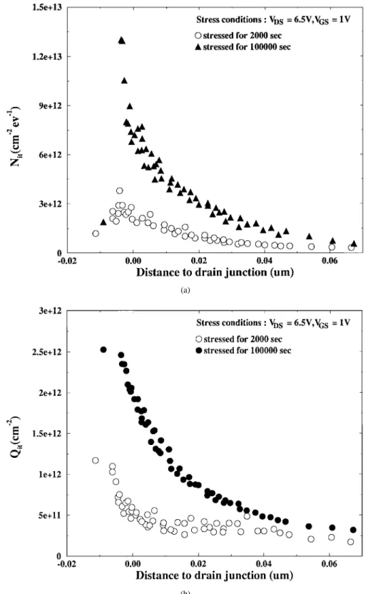
Fig. 7. The extracted (a) interface-trap density and (b) effective oxide-trapped charges for different stress times.
unstressed case, but (19) and (23) are used for and extractions. Because serious positive oxide-trapped charges are found after stress and the change of the surface potential near the drain junction cannot be ignored. Therefore, the iteration process mentioned in the previous section is necessary to obtain the accurate distribution. At the beginning, the function of the unstressed device is used to calculate and
, and after four iterations, the calculated and values
have converged to the stable values, and the values derived from different measuring conditions are shown to be self-consistent, as shown in Fig. 5. The distribution derived from (20) is shown in Fig. 6 and is compared to that derived from (19), it is obvious that the difference appears at the proximity of the drain junction because of the inharmonious distribution near the drain junction. Therefore, (20) is a good approximation only for the case with smooth
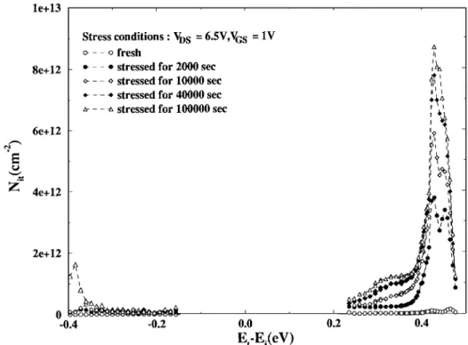
Fig. 8. The measured interface-trap density distribution in the bandgap for different stress times.
distribution. Note that the similar “effective area” approach for (20) had been used in all previous works to extract the spatial distribution, and this approach could induce obvious error because the peak of the distribution will be smoothed out. The and distributions after several stress times are shown in Fig. 7. Although the structure parameters shown in Table I have two decades numeral, they are only used to determine the reference point (“0” point) in lateral. The spatial distributions of interface-trap and effective oxide-trapped charge densities relative to the reference point (“0” point) are computed iteratively by the charge-pumping equa-tions given in Section II from the measured charge-pumping data; therefore, the resolution of three-decades numeral can be obtained. Note that the peak profiled by our novel charge-pumping technique isn’t located at the lateral drain junction, but is located in the gate-overlapped drain. This phenomenon is reasonable because the nonlocal effect [17], [18] of hot electrons will displace the peak distribution of hot electrons from the peak lateral electric field. The distance from the lateral drain junctions and the generated peak interface traps is about 0.003 m (30 ˚A) and this magnitude is approximately equal to the mean-free-path of hot electron and optical surface-phonon scattering.
C. Energy Distribution of in the Bandgap
Assuming that the energy distribution is independent of the spatial position, the distribution of in the upper part of the bandgap can be expressed as [11]
(24)
and that in the lower part of the bandgap can be expressed as (25)
Note that measuring the energy distribution of interface traps after the hot-carrier stress is useful for the 2-D numerical simulation of the stressed characteristics. The extracted distributions related to several stress times are shown in Fig. 8. There appear two peaks in the upper band, this means that there are two kinds of major interface-traps generated during the hot-carrier stress.
IV. CONCLUSIONS
An accurate and reliable charge-pumping method using dc source/drain biases is developed to extract the lateral distribu-tions of both interface-trap and effective oxide-trapped charge densities. Using the specified gate pulses with fixed , and the varied with , the smooth
curves related to a localized area near the drain(source) junction can be easily obtained and the interface-trap and effective oxide-trapped charge densities related to this area can be calculated at the same time. The effects of the hot-carrier-stress induced and on the surface potential are considered in this work to derive the accurate results. It is shown that the and distributions derived from different or are self-consistent. It should be emphasized that the developed method can also be applied to p-channel or LDD MOSFET’s. Therefore, the developed novel charge-pumping method will give the accurate analysis of the hot-carrier
LI et al.: NOVEL CHARGE-PUMPING METHOD 791
generated interface-trap and oxide-traps, which becomes the basis for future hot-carrier lifetime prediction.
REFERENCES
[1] P. Heremans, J. Witters, G. Groeseneken, and H. E. Maes, “Analysis of the charge pumping technique and its application for the evaluation of MOSFET degradation,” IEEE Trans. Electron Devices, vol. 36, pp. 1318, 1989.
[2] J. S. Burgler and P. G. Jespers, “Charge pumping in MOS devices,” IEEE Trans. Electron Devices, vol. ED-16, pp. 297, 1969.
[3] A. B. Elliot, “The use of charge pumping currents to measure surface state densities in MOS transistors,” Solid-State Electron, vol. 19, pp. 241, 1976.
[4] T. J. Russ L. Wilson, and M. Gaitan “Determination of the spacial variation of interface trapped charge using short-channel MOSFET’s,” IEEE Trans. Electron Devices, vol. ED-30, pp. 1662, 1983.
[5] G. Groeseneken, H. Maes, N. Beltran, and R. DeKeersmaecker, “A reliable approach to charge-pumping measurements in MOS transistors,” IEEE Trans. Electron Devices, vol. ED-31, pp. 42, 1984.
[6] U. Cilingiroglu, “A general model for interface-trap charge-pumping effects in MOS devices,” Solid-State Electron., vol. 28, pp. 1127, 1985. [7] W. L. Tseng, “A new charge pumping method of measuring Si-SiO2
interface states,” J. Appl. Phys., vol. 62, pp. 591, 1987.
[8] F. Hofmann and W. H. Krantschneider, “A simple technique for determining the interface trap distribution of submicron MOS transistors by the charge pumping method,” J. Appl. Phys., vol. 65, pp. 1358, 1989. [9] J. E. Chung and R. S. Muller, “The development and application of a Si-SiO2 interface-trap measurement system based on the staircase charge-pumping technique,” Solid-State Electron., vol. 32, pp. 867, 1989.
[10] N. S. Saks and M. G. Ancona, “Determination of interface trap capture cross sections using three-level charge pumping,” IEEE Electron Device Lett., vol. 11, pp. 339, 1990.
[11] G. Van den Bosch, G. V. Groeseneken, P. Heremans, and H. E. Maes, “Spectroscopic charge pumping: A new procedure for measuring interface trap distributions on MOS transistors,” IEEE Trans. Electron Devices, vol. 38, pp. 1820, 1991.
[12] M. G. Ancona, N. S. Saks, and D. McCarthy, “Lateral distribution of hot-carrier-induced interface traps in MOSFET’s,” IEEE Trans. Electron Devices, vol. 35, pp. 2221, 1988.
[13] W. Chen and T. P. Ma, “A new technique for measuring lateral distri-bution of oxide Charge and Interface traps near MOSFET junctions,” IEEE Electron Device Lett., vol. 12, pp. 393, 1991.
[14] H. H. Li and C. Y. Wu, “A new simplified charge-pumping current model and its model parameter extraction,” IEEE Trans. Electron Devices, vol. ED-43, p. 1857, 1996.
[15] P. Habas, “Charge-pumping characteristics of virgin and stressed lightly doped drain MOSFET’s,” Solid-State Electron., vol. 33, pp. 287, 1995. [16] H. H. Li and C. Y. Wu, “A novel extraction technique for the effective channel length of MOSFET devices,” IEEE Trans. Electron Devices, vol. 42, pp. 856, 1995.
[17] N. Goldsman and J. Frey, “Efficient and accurate use of the energy transport method in device simulation,” IEEE Trans. Electron Devices, vol. 35, pp. 1524, 1988.
[18] D. Chen, E. C. Kan, U. Ravaioli, C. W. Shu, and R.W. Dutton, “An improved energy transport model including nonparabolicity and non-Maxwellian distribution effects,” IEEE Electron Device Lett., vol. 13, pp. 26, 1992.
Hsin-Hsien Li (S’87) was born in Taiwan, R.O.C., in 1964. He received the B.S. degree from the De-partment of Electrical Engineering, National Cheng Kung University, Taiwan, in 1986, and the M.S. and Ph.D. degrees from the Institute of Electronics, National Chiao-Tung University, Hsinchu, Taiwan, in 1988 and 1995, respectively. His major research area was on device physics and reliability of deep-submicrometer MOSFET’s.
He is currently working with Silicon-Based Tech-nology Corporation, Hsinchu, and engages in device physics and circuit design of flash memory.
Mr. Li is a member of Phi Tau Phi.
Yu-Lin Chu (S’91) was born in Taiwan, R.O.C., on September 10, 1968. He received the B.S. degree from the Department of Material Science and Engi-neering, National Tsing-Hua University, Taiwan, in 1991, and the M.S. degree from the Institute of Elec-tronics, National Chiao-Tung University, Hsinchu, Taiwan, in 1993. He is currently pursuing the Ph.D. degree at the same institute. His present research areas focuses on deep-semiconductor MOS device physics and reliability issues, especially the charge-pumping technique.
Ching-Yuan Wu (M’72) was born in Taiwan, R.O.C., on March 18, 1946. He received the B.S. degree from the Department of Electrical Engineering, National Taiwan University, Taipei, in 1968, and the M.S. and Ph.D. degrees from the State University of New York (SUNY) at Stony Brook, in 1970 and 1972, respectively.
During the 1972–1973 academic year, he was appointed as a Lecturer at the Department of Electrical Sciences, SUNY, Stony Brook. During the 1973–1975 academic years, he was a Visiting Associate Professor at National Chiao-Tung University (NCTU), Hsinchu, Taiwan. In 1976, he became a Full Professor in the Department of Electronics and the Institute of Electronics, NCTU. At NCTU, he had been the Director of Engineering Laboratories and Semiconductor Research Center from 1974 to 1980; the Director of the Institute of Electronics from 1978 to 1984; and the Dean, College of Engineering, from 1984 to 1990. He was a Principal Investigator of the National Electronics Mass Plan-Semiconductor Devices and Integrated-Circuit Technologies, from 1976 to 1979, and had been a Coordinator of the National Microelectronics Researches and High-Level Mean-Power Education Committee, National Science Council, R.O.C., from 1982 to 1988. He has been the Research Consultant of the Electronics Research and Service Organization (ERSO), ITRI. His research activities have been in semiconductor physics and modelings, Integrated-circuit designs and Technologies. His present research areas focus on the developments of efficient 2-D and 3-D simulators for deep-submicrometer semiconductor devices, design rules and optimization techniques for deep-submicrometer CMOS devices, and key technologies for deep-submicrometer CMOS devices. He has published over 180 papers in the semiconductor field and has served as a reviewer for international journals such as IEEE ELECTRONDEVICELETTERS, IEEE TRANSACTIONS ONELECTRONDEVICES, and Solid-State Electronics.
Dr. Wu is a member of the Honorary Editorial Advisory Board of Solid-State Electronics, a board member of the Chinese Engineering Society. a member of the Academic Review Committee, the Ministry of Education; and the chairman of the Technical Review Committee on Information and Microelectronics Technologies, the Ministry of Economic Affairs. He received the Academic Research Award in Engineering from the Ministry of Education (MOE), in 1979 and the Outstanding Scholar Award from the Chinese Educational and Cultural Foundation in 1985. He received the Outstanding Research Professor fellowship from the Ministry of Education and the National Science Council (NSC), R.O.C., from 1982 to 1995. He also received the Distinguished Engineering Professor Medal Award from the Chinese Engineering Society in 1992.