A strictly nonblocking network based on nonblocking 4
×
4
optical switches
Chi-Ping Lee
a,b,∗, Chien-Ping Chang
c, Jiun-Shiou Deng
d, Min-Hao Li
e, Ming-Feng Lu
e,
Yang-Tung Huang
f, Ping-Yu Kuei
baDepartment of Computer Science and Information Engineering, Minghsin University of Science and Technology, No. 1, Hsinshing Rd., Hsinfeng,
Hsinchu, 304, Taiwan, ROC
bDepartment of Electrical Engineering, National Defense University, Taiwan, ROC
cDepartment of Computer Science and Information Engineering, Ching Yun University, Taiwan, ROC
dDepartment of Opto-Electronic System Engineering, Minghsin University of Science and Technology, Taiwan, ROC eDepartment of Electronic Engineering, Minghsin University of Science and Technology, Taiwan, ROC
fDepartment of Electronics Engineering, National Chiao-Tung University, Taiwan, ROC
a r t i c l e i n f o Article history:
Received 15 March 2010
Received in revised form 10 January 2011 Accepted 24 February 2011
Available online 17 April 2011
Keywords:
Optical multistage network Polarization selective element Strictly nonblocking System insertion loss Routing algorithm
a b s t r a c t
Recently, the demand for communication has been growing rapidly. Hence, optical multistage network technologies are more appreciated nowadays. A double-layer network is a strictly nonblocking network, and it has the lowest system insertion loss of non-dilated networks. A Beneš network is a rearrangeably nonblocking network, and it has the same system insertion loss as a double-layer network. We have proposed the use of modified polarization selection elements (PSEs). The system insertion loss, number of drivers, and number of required components of a double-layer network could be reduced if it is constructed with modified PSEs. A nonblocking 4×4 optical switch with two stages of polarization selective elements has been presented in our previous study. Based on this nonblocking 4×4 optical switch, we propose a strictly nonblocking network structure which features even lower system insertion loss than those of a double-layer network and a Beneš network. The signal-to-noise ratio of the proposed network structure is a constant, and is higher than the constraint, although it is lower than that of the double-layer network. The number of major components of the proposed network is less than that of a double-layer network and larger than that of a Beneš network, since a Beneš network is rearrangeably nonblocking. We also offer a routing algorithm for the new proposed network; the time complexity of the routing algorithm is O(1).
© 2011 Elsevier B.V. All rights reserved.
1. Introduction
Recently, the demand for communication has increased greatly. High transmitting capacity is an important feature
∗Corresponding author at: Department of Computer Science and
Information Engineering, Minghsin University of Science and Technology, No. 1, Hsinshing Rd., Hsinfeng, Hsinchu, 304, Taiwan, ROC. Tel.: +886 936 780 792; fax: +886 3 559 1402.
E-mail addresses:[email protected],[email protected]
(C.-P. Lee).
of communication systems. Since the bit rate of optical communication systems is higher than that of electronic communication systems [1], optical multistage networks are receiving more and more attention nowadays. To support optical communication systems, several kinds of optical multistage network have been presented [1–17]. A double-layer network is a strictly nonblocking network, and it has the lowest system insertion loss among non-dilated networks. A Beneš network is a rearrangeably nonblocking network. It has the same system insertion loss but a smaller number of optical switching elements compared with a double-layer network.
1573-4277/$ – see front matter©2011 Elsevier B.V. All rights reserved.
To implement these optical multistage networks, several optical switch structures have been proposed, such as integrated electro-optic devices on Ti
:
LiNbO3(titanium diffused lithium niobate) material [18], a prism PBS (polarization beam splitter), and a holographic PBS [19,20]. An optical multistage network constructed with LiNbO3features the allocation of all of the optical switching
elements and interconnection lines on the same plane. This feature induces the crossover problem of interconnection lines. The crossovers not only increase the system insertion loss but also reduce the signal-to-noise ratio (SNR) [21]. Since the polarization selective elements (PSEs), such as the prism PBS and the holographic PBS, are three-dimensional (3D) switching elements, all interconnection lines between two adjacent stages are parallel if the locations of the PSEs are arranged accurately. We could delete all interconnection lines and eliminate the crossover problem by coupling the stages tightly [22–32].
PSEs are convenient for constructing optical multistage networks due to the above features. A nonblocking 4
×
4 optical switch has been presented in our research [32]. Based on this nonblocking 4×
4 optical switch, we propose a strictly nonblocking network in this study. This paper is organized as follows. First, three types of optical switching element with PSEs are introduced in Section2. In Section3, the properties of blocking and crosstalk are discussed. In Section4, a strictly nonblocking network structure is proposed. We then offer the routing algorithm for the strictly nonblocking network in Section5. Finally, a brief conclusion is given.2. Optical switching elements with PSEs
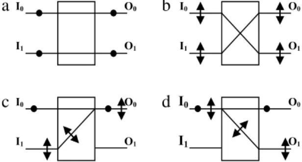
A 2
×
2 optical switching element with a PSE can have four possible switching states: ‘‘straight’’, ‘‘swap’’, ‘‘com-bine’’, and ‘‘split’’. The switching state is determined by the propagation direction of the PSE, which is determined by the polarization of the optical signal. These four states are shown inFig. 1. In the figures in this paper, s-polarization and p-polarization are denoted by ‘‘•
’’ and ‘‘↔
’’, respec-tively. InFig. 1(a), two s-polarized optical signals pass di-rectly through the PSE; thus it provides the ‘‘straight’’ state. InFig. 1(b), two p-polarized optical signals enter the PSE, and the propagation directions of these two p-polarized optical signals will be swapped by the PSE, so it provides the ‘‘swap’’ state. InFig. 1(c), two optical beams with dif-ferent polarizations enter the PSE from two separate input channels and depart from the same output channel; there-fore, it provides the ‘‘combine’’ state.Fig. 1(d) shows the opposite case. In this figure, two optical beams with differ-ent polarizations differ-enter the PSE from the same input chan-nel and depart from two separate output chanchan-nels, so it provides the ‘‘split’’ state.An electro-optic halfwave plate (EOHWP) is a compo-nent which can change the polarization of beam. An EO-HWP has two states: ‘‘active’’ and ‘‘inactive’’. An EOEO-HWP is in the ‘‘active’’ state when a voltage is applied to the EO-HWP. Otherwise, the EOHWP is in the ‘‘inactive’’ state. The beam through an EOHWP is changed from s-polarization to p-polarization or from p-polarization to s-polarization when the EOHWP is in the ‘‘active’’ state. In the other state,
Fig. 1. Four switching states of a 2×2 optical switching element with a PSE: (a) the ‘‘straight’’ state, (b) the ‘‘swap’’ state, (c) the ‘‘combine’’ state, and (d) the ‘‘split’’ state.
Fig. 2. The two switching states of a 2×2 optical switching element with one PSE and two EOHWPs: (a) the ‘‘straight’’ state, and (b) the ‘‘swap’’ state.
the EOHWP would not change the polarization of the pass-ing beam [33].
Shown inFig. 2 is a normal 2
×
2 optical switching element which is constructed by one PSE and two EOHWPs. The functions of the EOHWPs are twofold: to keep the polarization of the signals of the output channels the same as that of input channels, and to determine the switching state of the optical switching element. The switching element has two inputs (I0 and I1) and two outputs (O0and O1), and provides two switching states: one is the
‘‘straight’’ state and the other is the ‘‘swap’’ state. Each input (output) channel is passed by one optical signal; therefore, each interconnection line is passed by only one optical signal. A normal 2
×
2 optical switching element does not provide the ‘‘combine’’ state and the ‘‘split’’ state. We propose a modified 2×
2 optical switching element as shown inFig. 3. It is constructed by one PSE and four EOHWPs, and can provide the full states.A normal 1
×
2 optical switching element is constructed by one PSE and two EOHWPs, as shown in Fig. 4. The functions of the EOHWPs are the same as in a normal 2×
2 optical switching element. The 1×
2 switching element has one input (I) and two outputs (O0 and O1),and provides two switching states: a ‘‘straight’’ state and a ‘‘turn’’ state. We also propose a modified 1
×
2 optical switching element constructed by a PSE and an EOHWP; all of its possible switching states are shown in Fig. 5. BothFig. 5(a) and (b) show the ‘‘straight’’ state, and the output optical beams are s-polarized. BothFig. 5(c) and (d) show the ‘‘turn’’ state, and the output optical beams are p-polarized. Since the optical beam from the output channel could follow the same path backward with the corresponding polarization and finally reach the input channel, the 1×
2 optical switching element provides aFig. 3. The four switching states of a 2×2 optical switching element with one PSE and four EOHWPs: (a) the ‘‘straight’’ state, (b) the ‘‘swap’’ state, (c) the ‘‘combine’’ state, and (d) the ‘‘split’’ state.
Fig. 4. The two switching states of a 1×2 optical switching element constructed by a PSE and two EOHWPs: (a) the ‘‘straight’’ state and (b) the ‘‘turn’’ state.
Fig. 5. The four switching states of a 1×2 optical switching element constructed by a PSE and an EOHWP: (a) the ‘‘straight’’ state, (b) the ‘‘straight’’ state, (c) the ‘‘turn’’ state, and (d) the ‘‘turn’’ state.
bidirectional switching function. Therefore, a 1
×
2 optical switching element can act as a 2×
1 optical switching element.3. Optical multistage networks
3.1. Blocking properties
In general, there are four kinds of blocking property for switching networks: blocking, rearrangeably nonblocking, wide-sense nonblocking, and strictly nonblocking [34]. If there is no path to be established for a new legitimate request, we use the term blocking. If a legitimate request can be routed when some existing paths may be rerouted,
Fig. 6. A 4×4 blocking optical multistage network.
Fig. 7. (a) A 4×4 Beneš network, and (b) a 4×4 double-layer network.
we use the term rearrangeably nonblocking. If a legitimate request can be routed and no existing path needs to be rerouted when all connections are following a given routing algorithm, we use the term wide-sense nonblocking. If a legitimate request can be routed and all existing paths do not have to be rerouted regardless of how they are routed, we use the term strictly nonblocking.
3.1.1. Blocking optical multistage network
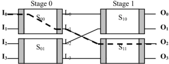
Fig. 6shows a 4
×
4 optical multistage network which has two stages of switching elements, and each stage has two 2×
2 optical switching elements, as shown in Fig. 1. In this structure, Lk,
Im, and On represent the kth interconnection line, mth input channel, and nthoutput channel, respectively, and Si−jrepresents the jth
switching element in the ith stage. Due to the fact that each interconnection line is only passed by one optical signal, input channel I1cannot be connected to output channel O3
when input channel I0is connected to output channel O2,
as shown inFig. 6. Therefore, it is a blocking network.
3.1.2. Nonblocking optical multistage networks
To solve the blocking problem, we have to use three stages of 2
×
2 optical switching elements to construct the networks, such as a 4×
4 Beneš network [3] and a 4×
4 double-layer network [1], as shown inFig. 7(a) and (b), respectively. Compared with the network shown in Fig. 6, a 4×
4 Beneš network has one more stage of 2×
2 optical switching elements and it provides nonblocking connection functions [32]. Similar to a 4×
4 Beneš network, a 4×
4 double-layer network has threeFig. 8. Two PSEs bound with one interconnection line.
Fig. 9. A nonblocking 4×4 optical switch.
stages of optical switching elements. However, the number of optical switching elements is doubled to provide a unique connection path for all permutations. Due to the unique feature, the double-layer network is strictly nonblocking. However, 4
×
4 Beneš and 4×
4 double-layer networks require more components and have higher system insertion loss than the network shown inFig. 4.3.1.3. A nonblocking 4
×
4 optical switchAs shown inFig. 8, we can bind two PSEs with one interconnection line. PSE0is the ‘‘combine’’ state and PSE1
is the ‘‘split’’ state. Two different polarized optical signals pass through the interconnection line L0 between PSE0
and PSE1at the same time. Therefore, the capacity of the
interconnection line L0has been increased, and the switch
can satisfy the nonblocking requirement. Utilizing these features, we can implement a nonblocking 4
×
4 optical switch with two stages of PSEs, as shown inFig. 9[32]. Ei−j,inFig. 9, represents the jth EOHWP of the ith stage.
3.2. Crosstalk
Most of the power of a signal passes through the desired path, but a small amount of the power does not; this is the crosstalk. We only discuss crosstalk occurring inside a PSE. When a signal passes through a PSE, we suppose that there is a part (
ε
) of the signal’s power that becomes crosstalk.3.2.1. Crosstalk in a 1
×
2 PSEFig. 10shows the crosstalk in a 1
×
2 PSE. As shown inFig. 10(a), the state of the PSE is the ‘‘straight’’ state. The s-polarized beam transmits from input I to output O0, and
there is
ε
Pinof the input beam that transmits to output O1which becomes crosstalk. The ‘‘turn’’ state, as shown in Fig. 10(b), is similar to the ‘‘straight’’ state, and the outputO0gains
ε
Pinof the p-polarized input beam, which is thecrosstalk.
3.2.2. Crosstalk in a 2
×
2 PSEA 2
×
2 PSE has four states, and the crosstalk of these states is illustrated inFig. 11.Fig. 11(a) shows the crosstalk of a 2×
2 PSE under the ‘‘straight’’ state. Two s-polarized beams transmit from input I0and I1to output O0and O1,respectively. Each beam has part (
ε
) of the signal powerFig. 10. The crosstalk in a 1×2 PSE: (a) the ‘‘straight’’ state and (b) the ‘‘turn’’ state.
Fig. 11. The crosstalk in a 2×2 PSE: (a) the ‘‘straight’’ state, (b) the ‘‘swap’’ state, (c) the ‘‘combine’’ state, and (d) the ‘‘split’’ state.
which transmits to another output, so each output has
ε
Pinof s-polarized crosstalk. The crosstalk of a 2×
2 PSEunder the ‘‘swap’’ state is shown inFig. 11(b). The signal of output O0consists of
(
1−
ε)
Pinof the p-polarized signalfrom input I1and
ε
Pinof p-polarized crosstalk from input I0. The output O1is similar to output O0. The crosstalk ofthe ‘‘combine’’ state is shown inFig. 11(c). The s-polarized signal beam enters into the PSE via input I0, then
(
1−
ε)
Pinof the signal departs from the PSE via output O0and
ε
Pinof the signal departs via output O1. The p-polarized signal
beam enters into the PSE via input I1, then
(
1−
ε)
Pinof thesignal departs from the PSE via output O0and
ε
Pinof thesignal departs via output O1. Therefore, the output O1has
2
·
ε
Pincrosstalk. The last case, shown inFig. 11(d), is thecrosstalk of the ‘‘split’’ state. The s-polarized signal beam and the p-polarized signal beam enter into the PSE via the same input I0. Then
(
1−
ε)
Pinsignal power of both beamsdeparts via output O0and O1, respectively. Meanwhile,
ε
Pinsignal power of both beams departs via output O1and O0,
respectively. Therefore, each output has
ε
Pincrosstalk. 3.2.3. Noise in a nonblocking 4×
4 optical switchThe first-order noise of a nonblocking 4
×
4 optical switch is shown inFig. 12; we neglect the higher-order crosstalk noise. As shown in Fig. 12(a), for either the ‘‘straight’’ state or the ‘‘swap’’ state, each output has 2·
ε
Pincrosstalk. InFig. 12(b), two PSEs are in the ‘‘combine’’ state and the others are in the ‘‘split’’ state. We can see that each output has 2
·
ε
Pincrosstalk, too. There are the same resultsin other permutation.
4. Strictly nonblocking networks with PSEs
We propose a new strictly nonblocking network which is constructed by the nonblocking optical switches shown
Fig. 12. First-order noise of a nonblocking 4×4 optical switch: (a) the ‘‘straight’’ state and the ‘‘swap’’ state and (b) the ‘‘combine’’ state and the ‘‘split’’ state.
in Figs. 3 and 9. In this section, the characteristics of the new proposed network, such as network structure, blocking property, numbers of PSEs and EOHWPs, system insertion loss, number of drivers, signal-to-noise ratio, and scalability, are discussed in detail. Then, we also compare the properties of this new proposed network with those of a double-layer network and a Beneš network.
4.1. Network structure
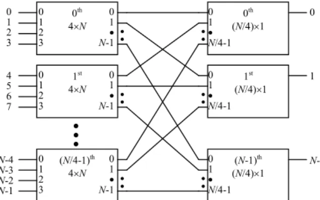
The basic structure of the new proposed N
×
N strictlynonblocking network is shown in Fig. 13. The network consists of two types of subnetwork: a 4
×
N subnetworkand an
(
N/
4) ×
1 subnetwork. The numbers of 4×
Nand
(
N/
4) ×
1 subnetworks are(
N/
4)
and N, respectively; there is one interconnection line to connect a given pair of 4×
N and(
N/
4)×
1 subnetworks. The network dimension of the proposed network structure is a multiple of 4, since we use the 4×
N subnetwork. An(
N/
4) ×
1 subnetwork consists of(
N/
4) −
1 2×
1 optical switching elements which are arranged in a(
k−
2)
-stage complete binary tree structure. The term k represents log2N. The basic structureof the 4
×
N subnetwork is shown inFig. 14; it consists of four 1×
2 optical switching elements and two 4×
(
N/
2)
subnetworks. This structure is a recursive structure. The basis of the 4×
N subnetwork is a nonblocking 4×
4 optical switch, shown inFig. 9. Therefore, the 4×
N subnetworkcan be divided into two parts: a 4
×
N optical beamsplitter and an
(
N/
4)
nonblocking 4×
4 optical switch. The 4×
N optical beam splitter consists of four 1×
(
N/
4)
optical beam splitters. Each 1×
(
N/
4)
optical beam splitter corresponds to an input channel, and each input channel can be completely connected to all nonblocking 4×
4 optical switches via a 1×
(
N/
4)
optical beam splitter. The 1×
(
N/
4)
optical beam splitter consists of(
N/
4) −
1 1×
2 optical switching elements arranged in a(
k−
2)
-stage complete binary tree structure. Fig. 15 shows a 4×
16 subnetwork which consists of four 1×
4 optical beam splitters and four nonblocking 4×
4 optical switches. In this figure, one of the 1×
4 optical beam splitters is indicated by dashed lines; it has three 1×
2 optical switching elements arranged in a two-stage complete binary tree structure.4.2. Blocking properties
For each connection, the optical signal will transmit through three parts: a 1
×
(
N/
4)
optical beam splitter, aFig. 13. The basic structure of an N×N strictly nonblocking network.
Fig. 14. The basic structure of a 4×N subnetwork.
Fig. 15. A 4×16 subnetwork.
nonblocking 4
×
4 optical switch, and an(
N/
4) ×
1 optical combiner (an(
N/
4)×
1 subnetwork). The 1×
(
N/
4)
opticalTable 1
The connection path table of a nonblocking 4×4 optical switch.
O0 O1 I0 E00→S00→E10→L0→S10→E20 E00→S00→E10→L0→S10→E21 I1 E01→S00→E10→L0→S10→E20 E01→S00→E10→L0→S10→E21 I2 E02→S01→E12→L2→S10→E20 E02→S01→E12→L2→S10→E21 I3 E03→S01→E12→L2→S10→E20 E03→S01→E12→L2→S10→E21 O2 O3 I0 E00→S00→E11→L1→S11→E22 E00→S00→E11→L1→S11→E23 I1 E01→S00→E11→L1→S11→E22 E01→S00→E11→L1→S11→E23 I2 E02→S01→E13→L3→S11→E22 E02→S01→E13→L3→S11→E23 I3 E03→S01→E13→L3→S11→E22 E03→S01→E13→L3→S11→E23
beam splitter is an active splitter switch and the
(
N/
4) ×
1 optical combiner is an active combiner switch. Both are strictly nonblocking [35]. The nonblocking 4×
4 optical switch will satisfy two conditions, unique feature and shareability of the first stage of the EOHWPs, if it is strictly nonblocking. The connection paths of the nonblocking 4×
4 optical switch are shown inTable 1. For each given pair of input and output, there is only one useful connection path; this means that the nonblocking 4×
4 optical switch has the unique feature. However, we need to prove that the operating state of the shared EOHWP is correct since some connection requests will use the same EOHWP of the first stage.Table 2shows the operating states of all EOHWPs of the first stage versus all connection requests. InTable 2, there are three terms: ‘‘I’’ represents the ‘‘inactive’’ state; ‘‘A’’ represents the ‘‘active’’ state; and blank represents the ‘‘don’t care’’ state. We find that the operating states are the same for a given pair of connection requests which share an EOHWP, and that they can exist concurrently. For example, there are two connection requests: I0→
O0and I1→
O1; both share an EOHWP, E10, and the operatingstates of E10are the same, ‘‘inactive’’. With the content of Table 2, we can prove the shareability of the first stage of the EOHWPs. Therefore, a nonblocking 4
×
4 optical switch is strictly nonblocking. Since all three parts are strictly nonblocking, the new proposed network is strictly nonblocking. We can prove this by contradiction. If the new proposed network is not strictly nonblocking, there is at least one part that needs to reroute the existing connection paths, and that part is not strictly nonblocking. This does not satisfy the known conditions. Therefore, the strictly nonblocking property of the new proposed network is proved.4.3. Numbers of PSEs and EOHWPs
The numbers of PSEs and EOHWPs are major cost factors. The number of 4
×
N subnetworks in the newproposed N
×
N strictly nonblocking network is(
N/
4)
. In a 4×
N subnetwork, the numbers of 1×
(
N/
4)
optical beam splitters and nonblocking 4×
4 optical switches are 4 andN
/
4, respectively. Each 1×
(
N/
4)
optical beam splitter has(
N/
4) −
1 1×
2 optical switching elements and each 1×
2 optical switching element is constructed by one PSE and one EOHWP. A nonblocking 4×
4 optical switch has 4 PSEs and 12 EOHWPs. The total numbers of PSEs and EOHWPs in a 4×
N subnetwork are(
2N−
4)
and(
4N−
4)
, respectively.Table 2
The operating states of all EOHWPs of the first stage versus all connection requests.
Request EOHWP E10 E11 E12 E13 I0→O0 I I0→O1 A I0→O2 A I0→O3 I I1→O0 A I1→O1 I I1→O2 I I1→O3 A I2→O0 A I2→O1 I I2→O2 I I2→O3 A I3→O0 I I3→O1 A I3→O2 A I3→O3 I
Hence, the numbers of PSEs and EOHWPs of all 4
×
Nsubnetworks are
(
N2/
2−
N)
and(
N2−
N)
, respectively.An
(
N/
4) ×
1 subnetwork consists of(
N/
4) −
1 2×
1 optical switching elements arranged in a(
log2N−
2)
-stage complete binary tree structure. The numbers of both PSEs and EOHWPs of an(
N/
4) ×
1 subnetwork are(
N/
4) −
1, as each 2×
1 optical switching element is constructed by one PSE and one EOHWP. Therefore, the numbers of both PSEs and EOHWPs of all(
N/
4) ×
1 subnetworks are(
N2/
4−
N)
. In total, the numbers of PSEs and EOHWPs inthe new proposed N
×
N strictly nonblocking network are(
3N2/
4−
2N)
and(
5N2/
4−
2N)
, respectively.4.4. System insertion loss
System insertion loss is an important constraint of system size; the system size could be larger if the system insertion loss were lower. 1
×
(
N/
4)
optical beam splitters and(
N/
4) ×
1 subnetworks have k−
2 stages of 1×
2 and 2×
1 optical switching elements, respectively. The system insertion loss is(
2k−
4)
LPSE+
(
2k−
4)
LEOHWP(in dB)in these two parts. In a nonblocking 4
×
4 optical switch, there are two stages of PSEs and three stages of EOHWPs, and the system insertion loss is 2LPSE+
3LEOHWP(in dB).Therefore, the system insertion loss of the new proposed
N
×
N network structure is(
2k−
2)
LPSE+
(
2k−
1)
LEOHWP(indB), where LPSEand LEOHWP(in dB) are the insertion losses
Fig. 16. An 8×8 strictly nonblocking network.
4.5. Number of drivers
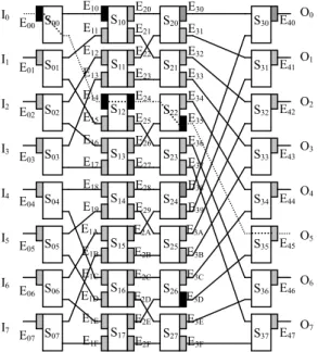
The number of drivers is a minor cost factor. Fig. 16
shows an 8
×
8 network structure with PSEs in which all EOHWPs have been numbered. We suppose that input I0isconnected to output O5; its connection path is indicated by
dash lines inFig. 16.
EOHWP10and EOHWP14are connected to the same 1
×
2optical switching element, S00. This 1
×
2 optical switchingelement only passes one optical signal to either EOHWP10
or EOHWP14. Therefore, EOHWP10and EOHWP14could be
set to the same state in any connecting case, and they need only one driver. There are eight pairs of EOHWPs in the first stage, and each pair needs one driver. Therefore, eight drivers are required. The EOHWPs in the third stage are in the same situation, so there are eight drivers, too. The EOHWPs in the zeroth and fourth stages, respectively, need eight drivers, since each EOHWP has to be controlled by an individual driver. Therefore, the EOHWPs in each stage, except the innermost stage, need eight drivers in an 8
×
8 strictly nonblocking network. In the innermost stage, the operating states of all EOHWPs are independent of each other. In this stage, the number of EOHWPs is 16, and the number of drivers is 16, too. In total, there are 48 drivers in an 8×
8 strictly nonblocking network.There are five stages of EOHWPs in an 8
×
8 strictly nonblocking network and(
2k−
1)
stages in an N×
Nstrictly nonblocking network. Except for the innermost stage, the EOHWPs in each stage need N drivers, and there are
(
2k−
2)
N drivers in subtotal. There are N2/
4 driversin the innermost stage. The total number of drivers is
(
N2/
4) +
2kN−
2N. 4.6. Signal-to-noise ratioThe noise comes from the crosstalk of each switching element. We only discuss the first-order noise, the major
Fig. 17. The worst case of SNR of an 8×8 strictly nonblocking network.
noise, and eliminate the higher-order noise. We show the worst case of signal-to-noise ratio of an 8
×
8 network as shown inFig. 17. Suppose that there are eight connection requests: inputs(
I0,
I1,
I2,
I3,
I4,
I5,
I6,
I7)
to outputs(
O0,
O2,
O1,
O3,
O4,
O7,
O6,
O5)
. The connection diagramis shown is Fig. 17. The bold lines present the signal paths, the solid arrows represent the major s-polarization noise paths, and the dotted arrows represent the major
p-polarization noise paths. InFig. 17, we only show the major noise of connection
(
I0,
O0)
. At output O0, there is3
·
ε
Pinnoise in total, which consists of 2·
ε
Pins-polarizationnoise and
ε
Pinp-polarization noise. We can eliminate the p-polarization noise by adding a polarizer at output O0(asshown inFig. 17); therefore, there is ultimately 2
·
ε
Pins-polarization noise. Hence, the signal-to-noise ratio of the proposed network structure is 10 log10
(
1/(
2·
ε)) = |
X| −
3 [36]
(|
X| =
10 log10(
1/ε))
.With a nonblocking 4
×
4 optical switch, the four input channels are connected to four 1×
(
N/
4)
optical beam splitters, and the four output channels are connected to four(
N/
4) ×
1 optical combiners. The signal is first transmitted into a 1×
(
N/
4)
optical beam splitter. A 1×
(
N/
4)
optical beam splitter has(
N/
4)
outputs and the power of the signals of all output channels forms a binomial distribution: one(
1−
ε)
k−2Pin
, (
k−
2)ε(
1−
ε)
k−3Pin, . . . , one
ε
k−2Pin. These output signals are the inputsignals of the nonblocking 4
×
4 optical switches. All input signals’ power of a nonblocking 4×
4 optical switch may be expressed as(
1−
ε)
k−2Pinsimultaneously, since the four
input signals come from four different 1
×
(
N/
4)
optical beam splitters. The output of a nonblocking 4×
4 optical switch has the largest noise power, 2·
ε
Pin, in this situation.Otherwise, the output has lower noise power or is pure noise. The output signals of a nonblocking 4
×
4 optical switch will transmit into the(
N/
4) ×
1 optical combiners. A(
N/
4) ×
1 optical combiner has N/
4 input channels, and its all input signals come from different nonblocking 4×
4 optical switches. A(
N/
4) ×
1 optical combiner isconstructed by
(
N/
4−
1)
2×
1 optical switching elements, arranged in a(
k−
2)
-stage complete binary tree structure. The output signal power of a 2×
1 optical switching element is(
1−
ε)
times the input signal power at most, no matter what the polarization of the input signal is (as shown inFig. 18). Therefore, the output signal power of a(
N/
4) ×
1 optical combiner is(
1−
ε)
k−2times the inputsignal power at most, since there are k
−
2 stages of 2×
1 optical switching elements. At most one s-polarization input signal and at most one p-polarization input signal could be transmitted to the output of a
(
N/
4) ×
1 optical combiner with the routing algorithm which is proposed in Section5.Fig. 19shows an example of a 4×
1 optical combiner. There is one s-polarization signal and one p-polarization signal to be transmitted to the output. The main input signal becomes an s-polarization signal when it departs from the output of the(
N/
4)×
1 optical combiner, no matter what its original polarization is. Meanwhile, at most one first-order noise input, which has different polarization than that of the main input signal, will become a p-polarization signal and depart from the output. We could eliminate this noise by a polarizer.4.7. Characteristics comparison
A double-layer network has the lowest system insertion loss of non-dilated networks [1]. We have proposed modified polarization selection elements. When a double-layer network is constructed with modified PSEs, its system insertion loss, number of drivers, and number of required components have been reduced [31]. Compared with such a double-layer network constructed by PSEs, the new proposed network structure has even lower system insertion loss and fewer major components. Meanwhile, we make a comparison between the new proposed network structure with a Beneš network constructed with PSEs. The new proposed network structure has lower system insertion loss but the Beneš network has fewer major components since it is a rearrangeably nonblocking network. The signal-to-noise ratios of a double-layer network and a Beneš network are
|
X|
[36] and|
X| −
10 log10
(
2k−
1)
[37] (in dB), respectively. A comparison of the characteristics between these network structures is shown inTable 3.4.8. Scalability
The transmission of a PSE is
η
PSE=
0.
9 [38], where thePSE is constructed by a prism PBS, and the transmission of an EOHWP is
η
EOHWP=
0.
85 [39]. Therefore, the systeminsertion losses LPSEand LEOHWPare 0.46 and 0.71 (in dB),
respectively, and the system insertion loss of the new proposed N
×
N network structure is 2.
43 log2N−
1.
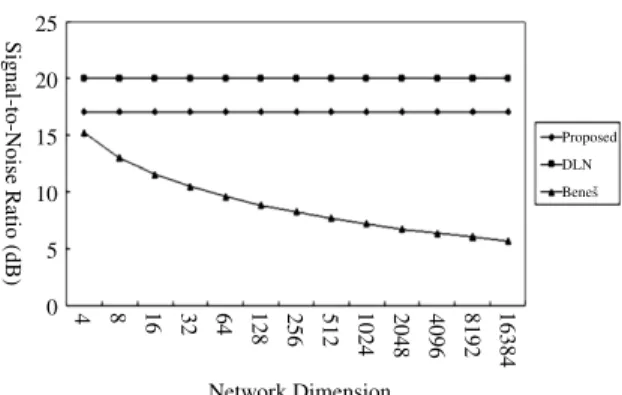
63. We assume that the system insertion loss is allowed to be 30 dB [37].Fig. 18shows the system insertion loss versus network dimension. We can see that the system insertion loss is over 30 dB when the network dimension is 16 384. For the signal-to-noise ratio, we suppose that|
X| =
20 dB andε =
10−2 [37]. The bit error rate is greater than10−9when the signal-to-noise ratio is less than 11 dB [37].
The signal-to-noise ratio versus the network dimension is shown inFig. 19.
Fig. 18. The system insertion loss versus network dimension.
Fig. 19. The signal-to-noise ratio versus network dimension.
5. Routing algorithm
In this section, we offer a routing algorithm for the new proposed strictly nonblocking network. We first introduce four terms used in the algorithm. The first term is
(
i)
j,which represents the jth bit of integer i; then i
=
(
i)
k−1(
i)
k−2. . . (
i)
0, and(
i)
j:m=
(
i)
j(
i)
j−1. . . (
i)
m. Thesecond term is S, which represents the source address of a connection. The third term is D, which represents the destination address of a connection. The last term is k, which represents log2N.
5.1. Routing algorithm
There are three arrays, Left, Middle, and Right, used in the routing algorithm. These arrays are used to control all drivers of the new proposed network. Array Left controls the drivers from the zeroth stage to the
(
k−
2)
th stage; array Middle controls the drivers of the(
k−
1)
th stage; and array Right controls the drivers from the kth stage to the(
2k−
2)
th stage. Array Left is a two-dimensional array, whose first index maps the stage of drivers and whose second index maps the input channel. For the first index, 0 maps the zeroth stage, 1 maps the first stage, and so on. For the second index, 0 maps input channel I0, 1 maps inputchannel I1, and so on. Array Middle is a one-dimensional
array, whose index maps the number of drivers in the
(
k−
1)
th stage. Array Right is a two-dimensional array, whose first index maps the stage of drivers and whose second index maps the output channel. For the first index, 0 maps the(
2k−
2)
th stage, 1 maps the(
2k−
3)
th stage, and so on. For the second index, 0 maps outputSignal-to-noise ratio |X| −3 |X| |X| −10 log10(2k−1)
Number of drivers N2/4+2kN−2N 2kN kN−N/2
Blocking property Strictly nonblocking Strictly nonblocking Rearrangeably nonblocking
channel O0, 1 maps output channel O1, and so on. When
the value of the entry is ‘‘false’’, the operating state of the EOHWP, which is controlled by the corresponding driver, is ‘‘inactive’’. Otherwise, the operating state of the EOHWP is ‘‘active’’. The data structures and the algorithm are shown as follows. Each expression can be executed merely from the source and destination addresses, not from the results of other expressions. Therefore, all expressions could be executed in parallel, and the time complexity of the routing algorithm is O
(
1)
.Data structures:
BooleanLeft
[
k−
1][
N]
,Middle[
N∗N/
4]
,Right[
k−
1][
N]
;Algorithm:
The zeroth stage: Left
[
0][
S] =
(
D)
k−1;Form the first stage to the
(
k−
3)
th stage Left[
i][
S] =
(
D)
k−iXOR(
D)
k−i−1;
(
1≤
i≤
k−
3)
The
(
k−
2)
th stageLeft
[
k−
2][
S] =
(
D)
2XOR(
D)
1XOR(
S)
0;The
(
k−
1)
th stageMiddle
[
(
S)
∗(k−1):2N+
(
D)
∗(k−1):24+
(
S)
∗12+
(
D)
1]
=
(
S)
1XOR(
S)
0XOR(
D)
1XOR(
D)
0;The kth stage
Right
[
0][
D] =
(
S)
k−1;Form the
(
k+
1)
th stage to the(
2k−
3)
th stage Right[
i][
D] =
(
S)
k−iXOR(
S)
k−i−1;
(
1≤
i≤
k−
3)
The
(
2k−
2)
th stageRight
[
k−
2][
D] =
(
S)
2XOR(
S)
1XOR(
D)
0;5.2. Deduction
For a given connection request
(
S,
D)
, we need to know two things: which EOHWP to operate and the operating state of the EOHWP.Each EOHWP is controlled by a driver. Therefore, instead of finding which EOHWP to operate, we can find which driver to operate. The number of the operating driver in the zeroth stage is the source address S, since the source address S is the number of the corresponding input channel, and the number of the driver in the zeroth stage is the number of the corresponding input channel, too. The numbers of the operating drivers from the first stage to the
(
k−
2)
th stage are the same as those in the zeroth stage.Table 4
The location of the operating driver versus the source and destination addresses of a nonblocking 4×4 optical switch.
S D 0(O0) 1(O1) 2(O2) 3(O3) 0(I0) 0(E10) 0(E10) 1(E11) 1(E11) 1(I1) 0(E10) 0(E10) 1(E11) 1(E11) 2(I2) 2(E12) 2(E12) 3(E13) 3(E13) 3(I3) 2(E12) 2(E12) 3(E13) 3(E13)
Fig. 20. The location of a nonblocking 4×4 optical switch.
The number of the operating driver in the
(
2k−
2)
th stage is the destination address D, since the destination addressD is the number of the corresponding output channel and
the number of the driver in the
(
2k−
2)
th stage is the number of the corresponding output channel, too. The numbers of the operating drivers from the kth stage to the(
2k−
3)
th stage are the same as for the(
2k−
2)
th stage. Each EOHWP in the(
k−
1)
th stage needs its own driver. The EOHWPs in the(
k−
1)
th stage of the new proposed network are the collection of the EOHWPs in the first stage of the nonblocking 4×
4 optical switches. We shall first find the operating driver in the first stage of the nonblocking 4×
4 optical switch. As shown inTable 4, we can locate the operating driver versus the source and destination addresses of the nonblocking 4×
4 optical switch fromTable 1. We can derive that the location of the operating driver is(
S)
∗12+
(
D)
1. Each connection will passthrough a nonblocking 4
×
4 optical switch; the location of the switch is shown inFig. 20. The nonblocking 4×
4 optical switch is the yth switch of the xth 4×
N subnetwork,where x is equal to
⌊
S/
4⌋ =
(
S)
k−1:2, and y is equal to⌊
D/
4⌋ =
(
D)
k−1:2. For the(
k−
1)
th stage, each 4×
Nsubnetwork contains N EOHWPs, and each nonblocking 4
×
4 optical switch contains four EOHWPs. Therefore, the number of the operating driver in the(
k−
1)
th stage is equal to(
S)
∗(k−1):2N+
(
D)
∗(k−1):24+
(
S)
∗12+
(
D)
1.The operating states of EOHWPs in the zeroth stage are determined by the polarization of the signals of the zeroth stage of the PSEs, and the operating states of the EOHWPs in the
(
2k−
2)
th stage are determined by the polarization of the signals of the(
2k−
3)
th stage of the PSEs. TheTable 5
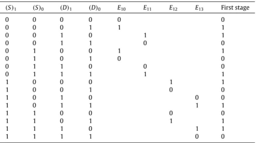
Truth table of the EOHWPs in the zeroth stage of a nonblocking 4×4 optical switch. (S)1 (S)0 (D)1 (D)0 E00 E01 E02 E03 Zeroth stage 0 0 0 0 0 0 0 0 0 1 0 0 0 0 1 0 1 1 0 0 1 1 1 1 0 1 0 0 1 1 0 1 0 1 1 1 0 1 1 0 0 0 0 1 1 1 0 0 1 0 0 0 0 0 1 0 0 1 0 0 1 0 1 0 1 1 1 0 1 1 1 1 1 1 0 0 1 1 1 1 0 1 1 1 1 1 1 0 0 0 1 1 1 1 0 0 Table 6
Truth table of the EOHWPs in the first stage of a nonblocking 4×4 optical switch. (S)1 (S)0 (D)1 (D)0 E10 E11 E12 E13 First stage 0 0 0 0 0 0 0 0 0 1 1 1 0 0 1 0 1 1 0 0 1 1 0 0 0 1 0 0 1 1 0 1 0 1 0 0 0 1 1 0 0 0 0 1 1 1 1 1 1 0 0 0 1 1 1 0 0 1 0 0 1 0 1 0 0 0 1 0 1 1 1 1 1 1 0 0 0 0 1 1 0 1 1 1 1 1 1 0 1 1 1 1 1 1 0 0
operating states of the other EOHWPs are determined by the polarization of the signals of the adjacent PSEs. The polarization of the signal of each stage of the PSEs is determined by the routing path, and the routing path is determined by the address. The routing path of a 1
×
(
N/
4)
optical beam splitter is determined by the destination address. When(
D)
i equals 0, where i is between 2 and(
k−
1)
, the signal’s polarization in the corresponding PSE (in the(
k−
i−
1)
th stage) is s-polarization; otherwise it is p-polarization. As regards the PSEs, the polarization expression of the ith stage is(
D)
k−i−1, where i is between0 and
(
k−
3)
. Therefore, the expression of the zeroth stage of drivers is(
D)
k−1and the expression of the ith stage is(
D)
k−iXOR(
D)
k−i−1, where i is between 1 and(
k−
3)
. Therouting path in an
(
N/
4) ×
1 combiner is determined by the source address. By the same method, the expression of the drivers in the(
2k−
2)
th stage is(
S)
k−1 and theexpression of the
(
2k−
2−
i)
th stage, 1≤
i≤
(
k−
3)
, is(
S)
k−iXOR(
S)
k−i−1. Table 5 shows the truth table ofthe operating states of the EOHWPs in the zeroth stage of a nonblocking 4
×
4 optical switch. The meaning of the value in each entry is as follows: 0 represents the ‘‘inactive’’ state; 1 represents the ‘‘active’’ state; and blank represents the ‘‘don’t care’’ state. The ‘‘Zeroth stage’’ field is the combined result from the ‘‘E00’’ field to the ‘‘E03’’field. We can get the general expression of the zeroth stage as
(
D)
1XOR(
S)
0. Therefore, the general expressionof the
(
k−
2)
th stage of the new proposed network is(
D)
2XOR(
D)
1XOR(
S)
0, since we need to consider thesignal’s polarization of the
(
k−
3)
th stage of the PSEs.Table 6shows the truth table of EOHWPs in the first stage; the ‘‘First stage’’ field is the combined result from the ‘‘E10’’
field to the ‘‘E13’’ field. We can get the general expression
of the first stage as
(
S)
1XOR(
S)
0XOR(
D)
1XOR(
D)
0, andthe general expression of the
(
k−
1)
th stage of the new proposed network is the same. Table 7shows the truth table of EOHWPs in the second stage; the ‘‘Second stage’’ field is the combined result from the ‘‘E20’’ fieldto the ‘‘E23’’ field. We can get the general expression of
the second stage as
(
S)
1XOR(
D)
0. Therefore, the generalexpression of the kth stage of the new proposed network is
(
S)
2XOR(
S)
1XOR(
D)
0, since it needs to consider thesignal’s polarization of the
(
k+
1)
th stage of the PSEs.6. Conclusion
A double-layer network is a strictly nonblocking network, and it has the lowest system insertion loss of non-dilated networks. A Beneš network has the same system insertion loss as a double-layer network, and it is
0 1 0 0 0 0 0 1 0 1 1 1 0 1 1 0 0 0 0 1 1 1 1 1 1 0 0 0 1 1 1 0 0 1 0 0 1 0 1 0 1 1 1 0 1 1 0 0 1 1 0 0 1 1 1 1 0 1 0 0 1 1 1 0 1 1 1 1 1 1 0 0
a rearrangeably nonblocking network. We have presented a double-layer network which could reduce the system insertion loss, number of drivers, and number of required components if it is constructed with modified PSEs which have been presented in our previous study. And we have proposed a nonblocking 4
×
4 optical switch and a modified 1×
2 optical switching element with PSEs. Based on these switches, a strictly nonblocking network structure has been proposed in this paper. Compared with a double-layer network with PSEs, the numbers of PSEs and EOHWPs of the proposed network are significantly reduced, by 40% and 37.5%, respectively. But they are still larger than for a Beneš network since a Beneš network is a rearrangeably nonblocking network. In addition, the system insertion loss is LPSE+
LEOHWP (in dB) less than that in adouble-layer network and LPSE
+
(
2 log2N−
1)
LEOHWP (in dB)less than that in a Beneš network, respectively. The signal-to-noise ratio of the new proposed network structure is
|
X| −
3 (in dB). It is a constant and higher than the constraint, although it is lower than the signal-to-noise ratio of a double-layer network. The number of drivers isN2
/
4+
2N log2N
−
2N, which is larger than for both adouble-layer network and a Beneš network. We also offer a routing algorithm for the new proposed network; the time complexity of the routing algorithm is O
(
1)
.References
[1] C.C. Lu, R.A. Thompson, The double-layer network architecture for photonic switching, IEEE Transactions on Lightwave Technology 12 (1994) 1482–1489.
[2] C. Clos, A study of nonblocking switching networks, Bell System Technical Journal (1953) 407–424.
[3] V.E. Beneš, Mathematical Theory of Connecting Networks and Telephone Traffic, Academic, New York, 1965.
[4] T. Lang, H.S. Stone, A shuffle-exchange network with simplified control, IEEE Transactions on Computers 25 (1976) 55–65. [5] H.S. Hinton, A nonblocking optical interconnection network using
directional couplers, in: Proc. of GLOBECOM, 1984, pp. 885–889. [6] R.A. Spanke, Architectures for guided-wave optical space switching
systems, IEEE Communications Magazine 25 (1987) 42–48. [7] R.A. Spanke, V.E. Beneš, N-stage planar optical permutation network,
Applied Optics 26 (1987) 1226–1229.
[8] K. Padmanabhan, A. Netravali, Dilated networks for photonic switch-ing, IEEE Transaction on Communications 35 (1987) 1357–1367. [9] C.-T. Lea, Multi-log2N network and their applications in high-speed
electronic and photonic switching systems, IEEE Transaction on Communications 38 (1990) 1740–1749.
[10] T.H. Lee, S.J. Liu, Banyan network nonblocking with respect to cyclic shifts, Electronics Letters 27 (1991) 1474–1476.
[11] P. Giacomazzi, V. Trecordi, A study of nonblocking multicast switching network, in: Proc. of GLOBECOM, 1996, pp. 739–743. [12] W. Kabacinski, Modified dilated Beneš network for photonic
switch-ing, IEEE Transaction on Communications 47 (1999) 1087–1091. [13] J.-S. Deng, Y.-T. Huang, W.-Y. Wang, Clos network with cyclic
crossbar structure, in: Fiber and Optical Interconnection Network 2001, 2001.
[14] D.Z. Du, P. Fishburn, B. Gao, F.K. Hwang, Wide-sense nonblocking for 3-stage Clos networks, in: D.Z. Du, H.Q. Ngo (Eds.), Switching Networks: Recent Advances, Amsterdam, 2001.
[15] J.-S. Deng, Y.-T. Huang, Modified Beneš networks for photonic switching, in: Proc. of SPIE, vol. 4595, 2001, pp. 74–82.
[16] F.H. Chang, J.Y. Guo, F.K. Hwang, C.K. Lin, Wide-sense nonblocking for symmetric or asymmetric 3-stage Clos networks under various rout-ing strategies, Theoretical Computer Science 314 (2004) 375–386. [17] J.S. Deng, M.F. Lu, Y.T. Huang, Cyclic crossbar network for photonic
switching, Journal of Optical Networking 12 (4) (2004) 839–853. [18] J.E. Watson, M.A. Milbrodt, K. Bahadori, M.F. Dautartas,
C.T. Kemmerer, D.T. Moser, A.W. Schelling, T.O. Murphy, J.J. Veselka, D.A. Herr, A low-voltage 8×8Ti : LiNbO3switch with a
dilated-Beneš architecture, IEEE Journal of Lightwave Technology 8 (1990) 794–801.
[19] Y.T. Huang, Y.H. Chen, Polarization-selective element with a substrate-mode grating pair structure, Optics Letters 18 (1993) 921–923.
[20] J.S. Deng, M.F. Lu, C.P. Lee, Y.T. Huang, A high contrast ratio optical switch with holographic optical switching elements, WSEAS Transactions on Electronics 2 (2005) 33–38.
[21] C.-T. Lea, Crossover minimization in directional-couple-based pho-tonic switching systems, IEEE Transactions on Communications 36 (1998) 355–363.
[22] K.M. Johnson, M.R. Surette, J. Shamir, Optical interconnection network using polarization-based ferroelectric liquid crystal gates, Applied Optics 27 (1988) 1727–1733.
[23] A. Karppinen, S. Lottholz, R. Myllyla, G. Anderson, M. Matuszczyk, K. Skarp, I. Dahl, S.T. Lagerwall, Electrically controlled optical atten-uators and switches with ferroelectric liquid crystals, Ferroelectrics 114 (1991) 93–97.
[24] M. Kato, H. Ito, T. Yamamoto, F. Yamagishi, T. Nakagami, Multichan-nel optical switch that uses holograms, Optics Letters 17 (1992) 769–771.
[25] Y.-T. Huang, M.-F. Lin, J.-S. Deng, K.-T. Fan, M.-J. Chang, Holographic polarization-selective elements in optical network applications, in: Proc. of SPIE, vol. 2885, 1996, pp. 112–123. (Invited).
[26] M. Cao, Q. Hua, Z. Wana, F. Luo, A novel routing optical matrix switching method, Optics Communications 204 (2002) 163–170. [27] J.-S. Deng, M.-F. Lu, Y.-T. Huang, Double-layer networks with
holographic optical switches, Applied Optics 43 (2004) 1342–1348. [28] C.P. Lee, J.S. Deng, M.F. Lu, Y.T. Huang, Performance analysis of Beneš networks with high contrast ratio holographic optical switching elements, WSEAS Transactions on Communications 2 (5) (2006) 259–266.
[29] J.S. Deng, M.F. Lu, C.P. Lee, Y.T. Huang, AS/AC networks with holographic optical switching elements, International Journal of Microwave and Optical Technology 2 (1) (2006) 570–575.
[30] J.S. Deng, C.Y. Lee, M.F. Lu, Y.T. Huang, Loss reduction of AS/AC networks with holographic optical switches, in: The 7th WSEAS International Conference on Electric Power System, High Voltages, Electric Machines, Venice, Italy, Nov. 2007, pp. 21–24.
[31] J.S. Deng, H.H. Huang, M.F. Lu, Y.T. Huang, Loss reduction of double-layer networks with holographic optical switches, in: Proceedings of the 8th WSEAS International Conference on APPLIED COMPUTER SCIENCE, ACS’08, Venice, Italy, Nov. 2008, pp. 21–23.
[32] J.S. Deng, C.P. Lee, M.F. Lu, M.F. Lin, Y.T. Huang, 4 × 4 opti-cal switch with polarization selective elements, in: IEEE Interna-tional Conference on Networks, ICON 2006, Singapore, Sep. 2006, pp. 361–365.
[33] N.A. Riza, N. Madamopoulos, Characterization of a ferroelectric liquid crystal-based time delay unit for phased array antenna applications, Journal of Lightwave Technology 15 (7) (1997) 1088–1094.
[34] F.K. Hwang, A survey of nonblocking multicast three-stage Clos networks, IEEE Communications Magazine (2003) 34–37. [35] R.A. Spanke, Architecture of large nonblocking optical space
switches, IEEE Journal of Quantum Electronics 6 (QE–22) (1986) 964–967.
[36] M.H. Li, J.S. Deng, High performance strictly nonblocking network with polarization selection elements, Master Thesis, Minghsin University of Science and Technology, Taiwan, 2010.
[37] H. Tian, A.K. Katangur, J. Zhong, A novel multistage network architecture with multicast and broadcast capability, vol. 35, 2006, pp. 277–300.
[38]http://search.newport.com/?q=*&x2=sku&q2=05FC16PB.3. [39] N. Madamopoulos, N.A. Riza, Adaptable-delay balanced-loss binary
photonic delay line architectures using polarization switching, Optics Communications 152 (1998) 135–143.


![[102-2] WNFA lab4 - A Tiny Wireless Sensor Network](data:image/gif;base64,R0lGODlhAQABAIAAAP///wAAACH5BAEAAAAALAAAAAABAAEAAAICRAEAOw==)