An ultra-broadband nano-plasmonic reflector with an asymmetric
nano-ring resonator
Yuhsin Chang, and Chyong-Hua Chen
Department of Photonics and Institute of Electro-Optical Engineering,
National Chiao Tung University, 1001 University Road, Hsinchu 30010, Taiwan
ABSTRACT
We propose a broadband nano-plasmonic reflector by using an asymmetric nano-ring resonator directly connected to the input and output waveguides based on metal-insulator-metal waveguides. Due to direct connection, both clockwise and counterclockwise traveling modes propagate inside the ring resonator, giving rise to resonator resonances and Mach Zehnder interference. Ultra-broad bandwidth is realized by adjusting the lengths of the ring to manipulate the resonant wavelengths and varying its widths to minimize the low-transmission ripples. An example of the plasmonic reflector with the dimensions of 200×522 nm×nmand the bandwidth of 1000 nm is numerically accomplished
Keywords: Plasmonic waveguide, optical resonator, broadband reflector, integrated photonics 1. INTRODUCTION
Plasmonics provides a promising on-chip platform for the ultra-density photonic integrated circuits (PICs) because surface plasmon-polariton (SPP) modes are highly confined in the plasmonic waveguides at sub-wavelength scale1,2.
Among various plasmonic waveguides, metal-insulator-metal (MIM) waveguides have a potential for future ultra-density PICs due to strong field confinement of SPP modes, relatively low bending and propagation losses and easy fabrication 3-7. Plasmonic ring resonators based on MIM waveguides are essential components in the ultra-density PICs due to its
compactness, wide free-spectral range and potential in monolithic integration. Various devices with this scheme have been proposed and investigated, including Mach Zehnder interferences3, power splitters4, bandpass filters5, notch filters6
and sensors7. In this paper, we use an asymmetric plasmonic ring resonator to design a broadband reflector. This device
consists of a plasmonic nano-ring resonator directly connected to the input and output waveguides based on MIM waveguides. We use an equivalent circuit model to analyze the performance of this structure, and then observe that either Mach Zehnder interference3 (MZI) or the ring resonance6 (RR) results in high reflectance of the device. Subsequently,
we manipulate the resonant wavelengths of RR and of MZI for completely destructive interference in the output waveguide to achieve an ultra-broadband plasmonic reflector. Design example to obtain a broadband reflector with given specifications is numerically demonstrated, and simulation results show that this device has the dimensions of 200×522 nm×nm, the maximum reflectance of -0.8 dB and a bandwidth of 1000 nm.
2. BROADBNAD REFLECTOR
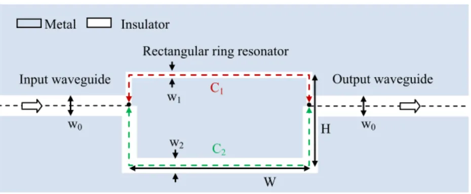
The structure of the proposed ultra-broadband nano-plasmonic reflector based on MIM waveguides is shown in Fig. 1. An asymmetric rectangular ring resonator with a width W and a height H is directly connected to the input and output waveguides. The waveguide width of the input and output waveguides are w0. Due to direct connection between the
input/output waveguides and the rectangular ring resonator, the rectangular ring resonator is divided into two branches C1 and C2. Let the waveguide width and the length of the branch Ci be wi and Li, respectively, for i=1 and i=2. Then,
Figure 1. Proposed structure for the ultra-broadband nano-plasmonic reflector.
Because the propagation behavior of MIM waveguides in optical region is similar to that of a parallel-plate transmission line in microwave domain8, we use the equivalent circuit model of the transmission line to analyze this proposed
structure. The characteristic impedances of the input and output waveguides are calculated by Z0=(β0w0)/(ωε0εd), where
β0 is the propagation constant, ω is the incident frequency, ε0 ispermittivity of free space and εd is relative permittivity of
the insulator. Each waveguide segment of the branch Ci is represented by a symmetric T-type equivalent circuit9 with the
impedances of Zia=jZitan(βiLi/2) and Zib=-jZi/sin(βiLi), where βi and Zi=(βiwi)/(ωε0εd) are the propagation constant and of
the characteristic impedance of the branch Ci, for i=1 and 2. Then, the equivalent input impedance of this structure is
illustrated in Fig. 2.
Figure 2. The equivalent input impedance of the proposed structure
This equivalent input impedance is then calculated by
0 0 ( a)( ) ,b in a a b Z Z Z Z Z Z Z Z + = + + + (1) where Za=Z1a+Z2a and Zb=Z1b+Z2b.
The reflectance of the proposed structure is expressed by10
2 2 2 2 0 0 2 2 0 0 0 0 2 2 2 2 in a b a in a b a b a Z Z Z Z Z Z R Z Z Z Z Z Z Z Z Z Z − − − = = + + + + + (2)
As shown in Fig. 2, we find that the maximum reflectance may be obtained as the load voltage at Z0 (i.e., the output port)
is zero in order to obtain zero transmission. Then, zero transmission is obtained as (i) β1L1=pπ and β2L2=(p+q)π, where p
is an integer and q is an odd number, or as (ii) Zb=0, that is Z1sin(β2L2)+Z2sin(β1L1)=0. In our proposed structure, the
wave inside the resonator can propagate either clockwise or anticlockwise owing to the impedance mismatch of the T-branch at each intersection. As the wave in the T-branches C1 and C2 propagates oppositely, MZI occurs. Contrarily, the
Z
2aZ
2aZ
2bZ
1aZ
1aZ
1bZ
0Z
in+
-
V
load Metal Insulator w0 w0 w2 w1 Input waveguide W H C1 C2Rectangular ring resonator
shows that the phase difference between the branches C1 and C2 is an odd multiple of π, as a consequence of destructive
interference of MZI in the output waveguide. On the other hand, the second condition shows the interference of the clockwise and anti-clockwise circulating waves inside the resonator is completely destructive in the output waveguide, where Z1 and Z2 are relevant to the transmission coefficients of the two branches in an opened T-branch splitter. This
expression corresponds to the condition of the zero-transmission RR.
Due to lossy SPP modes, these two conditions are too difficult to be satisfied, and thereby the transmission is impossible to reach zero. However, the high reflectance still can be obtained as real parts of the conditions are taken into account for a comparatively low loss structure, i.e., (i) Re{β1L1}=pπ and Re{β2L2}=(p+q)π, and (ii) Re{Z1sin(β2L2)+Z2sin(β1L1)}=0.
Then, in order to obtain a broadband reflector, we manipulate the resonant wavelengths of these two conditions. For a reflector with a squared reflection spectrum, the upper and lower edge wavelengths are λU and λL, respectively. Because
the difference between the adjacent resonant wavelengths of the RR is smaller than that of the MZI, the first- and second-order resonant wavelengths of the RR, λRR,1 and λRR,2, are assigned as λU and λL, respectively. The wavelength for
the destructive interference of the MZI λMZI is the center wavelength of the reflector because the reflection is rather
higher at λMZI than at λRR,1 and λRR,2 as a result of higher circulating propagation loss for the RR. The relative locations of
these resonant wavelengths are delineated in Fig. 3.
Then, to realize a broadband reflector, the design parameters of this structure can be obtained by satisfying the following conditions: 1 1 Re{ (β λMZI) }L =π (3) 2 2 Re{ (
β λ
MZI) } 2 ,L =π
(4){
1 RR,1 1 2 RR,1 2 2 RR,1 2 1 RR,1 1}
Reβ λ
( ) sin( (wβ λ
) )L +β λ
( ) sin( (wβ λ
) )L =0 (5){
1 RR,2 1 2 RR,2 2 2 RR,2 2 1 RR,2 1}
Reβ λ
( ) sin( (wβ λ
) )L +β λ
( ) sin( (wβ λ
) )L =0. (6)Figure 3. The relative location of the RR and MZI resonant wavelengths for a broadband reflector
3. SIMULATED RESULTS
Here, we use the Ag-air-Ag waveguides to demonstrate our design concepts. The permittivity of the silver εm is
described by the Drude-Lorentz model11. Suppose that the targeted reflector has edge wavelengths of 1450nm and
1650nm. Then, λRR,1=1650nm, λRR,2=1450nm and λMZI=1550nm. Because (3)-(6) show the conditions of the high
reflections are independent of w0, we arbitrarily choose w0 as 50 nm. In addition, (3)-(6) are related as the propagation
constant of the fundamental SPP mode for a fixed waveguide width is an approximately linear function of the wavelength λ. Then, we can arbitrarily choose w1 and find the corresponding L1 by (3). For example, let w1 be 16 nm
and then L1=383nm. Subsequently, we obtain w2 and L2 by numerically or graphically solving (5) and (6). The graphical
solution sets of {w2, L2} for (5) and (6) are shown in Fig. 4. These two curves intersect at {w2=43 nm, L2=1060 nm}, and
then w2 and L2 are set as 43 nm and 1060 nm, respectively. As we examine (4) with w2=43 nm and L2=1060 nm, the
20 40 60 80 800 900 1000 1100 1200 1300 w2 (nm) L 2 (n m )
Figure 4. Graphical solution sets {w2, L2} for (5) (solid curve) and (6) (dashed curve) with w1=16 nm, L1=383 nm, λRR,1=1650 nm and λRR,2=1450 nm .
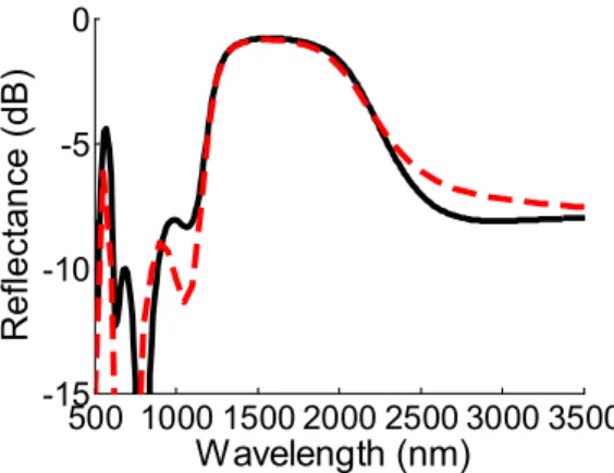
To avoid the coupling between two adjacent waveguides, the resonator width W is chosen as 200 nm, and then the corresponding height H is 522 nm, i.e., the dimensions of the rectangular waveguide is 200×522 nm×nm. The reflectance spectra of this reflector both calculated by (2) and simulated by two-dimensional (2D) finite-difference time domain (FDTD) method are shown in Fig. 5. A maximum reflectance of roughly -0.8 dB is obtained at the wavelength of λMZI=1550nm, and the reflectance is larger than -0.9 dB over the wavelength range of λRR,1=1650 nm and λRR,2=1450 nm.
These indicate that the high-reflectance region is expectedly obtained. The 3-dB bandwidth is approximately 1000 nm. In addition, the calculated data and simulated FDTD results are closely consistent with a small deviation outside of the high-reflectance band. 500 1000 1500 2000 2500 3000 3500 -15 -10 -5 0 Wavelength (nm) Refle ctan ce (d B)
Figure 5. Reflectance spectra of the proposed reflector calculated by the equivalent circuit model (solid black curve) and the FDTD method (dashed red curve) with w1=16 nm, L1=383 nm, w2=43 nm, and L2=1060 nm.
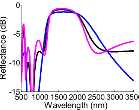
Next, we discuss the influence of w1 on the reflectance spectrum of a broadband reflector with the same design
specifications. The aforementioned procedure is applied to obtain the design parameters with different w1. Figure 6
shows the reflectance spectra for various designs with different w1. To obtain a reflector with the same specifications, we
find that the width of branch C2, w2, increases with the increase of w1. However, the dimension of the device becomes
larger as w1 increases. As shown in Fig. 6, the maximum reflectance decreases with the decrease of w1 because of rather
large propagation loss for a narrow MIM waveguide. Furthermore, the high-reflectance region becomes flat and the 3dB-bandwidth is broader as w1 decreases.
500 1000 1500 2000 2500 3000 3500 -15 -10 -5 0 Wavelength (nm) Refle ctan ce (d B)
Figure 6. The reflectance spectra of three designed reflectors, where w0=50 nm: w1=10 nm, L1=317 nm, w2=28 nm and L2=933 nm (blue curve); w1=16 nm, L1=383 nm, w2=43 nm, and L2=1060 nm (black curve); and w1=20 nm, L1=416 nm,
w2=53 nm, and L2=1117 nm (magenta curve)
4. CONCLUSION
We numerically present an asymmetric nano-ring resonator to realize an ultra-broadband plasmonic reflector. An analytical formulation to describe the performance of this structure is obtained by using the equivalent circuit model based on the transmission line theory. Subsequently, a systematic design procedure is developed to obtain the design parameters of the broadband reflector with given specifications. An example of the plasmonic reflector with the dimension of 200×522 nm×nmand the bandwidth of 1000 nm is numerically accomplished. The calculated results are validated with the simulated ones obtained by the 2D FDTD method. The performance of the device can be improved by increasing w1 with a rather large device's size.
REFERENCES
[1] Gramotnev, D. K. and Bozhevolnyi, S. I., "Plasmonic beyond the diffraction limit," Nature 4(2), 83-91 (2010). [2] Schuller, J. A., Barnard, E. S., Cai, W. S., Jun, Y. C., White, J. S. and Brongersma, M. L., "Plasmonics for
extreme light concentration and manipulation," Nature Materials 9(3), 193-204 (2010).
[3] Wang, B. and Wang, G. P., "Surface plasmon polariton propagation in nanoscale metal gap waveguides," Optics Letters 29(17), 1992–1994 (2004).
[4] Chen, C.-H. and Liao, K.-S., "1xN plasmonic power splitters based on metal-insulator-metal waveguides," Optics Express 21(4), 4036–4043 (2013).
[5] Swillam, M. A. and Helmy, A. S., "Feedback effects in plasmonic slot waveguides examined using a closed form model," IEEE Photonics Technology Letters 24(6), 497-499 (2012).
[6] Nezhad, V. F., Abaslou S. and Abrishamian, M. S., "Plasmonic band-stop filter with asymmetric rectangular ring for WDM networks," Journal of Optics 15, 055007 (2013).
[7] Bahramipanah, M., Abrishamian, M. S., Mirtaheri, S. A., and Liu, J.-M., "Ultracompact plasmonic loop-stub notch filer and sensor," Sensors and Actuators B 194, 311-318 (2014)
[8] Nejati, H. and Beirami, A., "Theoretical analysis of the characteristic impedance in metal-insulator-metal plasmonic transmission lines," Optics Letters 37(6), 1050-1052 (2012).
[9] Chang, K. and Hsieh, L.-H., [Microwave Ring Circuits and Related Structures ], 2nd edition, Wiley, New York,
24 (2004)
[10] Pozar, D. M., [Microwave Engineering], 4th edition, Wiley, New York, 29 (2011)
[11] Johnson, P. B., and Christy, R. W., "Optical constants of the noble metals," Physical Review B 6, 4370-4379 (1971).