國 立 交 通 大 學
電子工程學系 電子研究所
博 士 論 文
低溫製程技術應用於動態隨機存取記憶體之鈦酸鍶鋇
薄膜電容器之研究
Low-Temperature Processing Techniques Applied on
Barium Strontium Titanate Films for the Applications of
DRAM Storage Capacitors
研 究 生:史 德 智
指導教授:邱 碧 秀 博士
低溫製程技術應用於動態隨機存取記憶體之鈦酸鍶鋇
薄膜電容器之研究
Low-Temperature Processing Techniques Applied on
Barium Strontium Titanate Films for the Applications of
DRAM Storage Capacitors
研 究 生:史 德 智 Student: D. C. Shye 指導教授:邱 碧 秀 博士 Advisor: Dr. B. S. Chiou
國
立
交
通
大
學
電
子
研
究
所
博
士
論
文
A DissertationSubmitted to Institute of Electronics
College of Electrical Engineering and Computer Science National Chiao Tung University
in Partial Fulfillment of the Requirements for the Degree of
Doctor of Philosophy in Electronics Engineering
January, 2005
Hsinchu, Taiwan, Republic of China
推薦函
中華民國九十三年十二月十四日
事由: 推薦電子研究所博士班研究生史德智提出論文並參加國立交通大 學博士論文口試。 說明: 電子研究所博士班研究生史德智先生,業已修畢部訂所需學分,通 過博士資格考之學科考試,並完成博士論文初稿之撰寫,論文名稱為: 「低溫製程技術應用於動態隨機存取記憶體之鈦酸鍶鋇薄膜電容器之研 究」。博士論文內容中已有數篇期刊論文、會議論文及專利發表,同時尚 有數篇論文投稿中,準備發表於學術期刊。茲列舉如下:Journal Papers
1. Der-Chi Shye, Bi-Shiou Chiou, Ming-Jiunn Lai, Chuan-Chou Hwang, Cheng-Chung Jaing, Jyh-Shin Chen, Ming-Hwu Cheng, and Huang-Cheng-Chung Cheng, " Low-Temperature Radio-Frequency-Sputtered (Ba, Sr)TiO3 Films on Pt/TiN/Ti/Si
Substrates with Various Oxygen/Argon Mixing Ratios", Journal of The Electrochemical Society, vol. 150(2) p. F20-F27, 2003.
2. Der-Chi Shye, Jyh-Shin Chen*, Meng-Wei Kuo, Bruce C. S. Chou, Chueh-Kuei Jan, Mei-Fang Wu, Bi-Shiou Chiou and Huang-Chung Cheng, "Current-temperature Characteristics of Low-temperature-sputtered (Ba,Sr)TiO3 Films Post Treated by
Rapid Thermal Annealing", Integrated Ferroelectrics, vol. 47, pp.217-225, 2002. 3. Der-Chi Shye, Bi-Shiou Chiou, Meng-Wei Kuo, Jyh-Shin Chen, Bruce C. S. Chou,
Chueh-Kuei Jan, Mei-Fang Wu and Huang-Chung Cheng, " Polarization Dependence on Temperature-Coefficient-Resistance of (Ba, Sr)TiO3 Thin Films Post
Treated by Rapid Thermal Annealing", Electrochemical and Solid State Letters, vol. 6 (4), p. G55-G58, Apr. 2003.
4. Der-Chi Shye, Chuan-Chou Hwang, Ming-Jiunn Lai, Cheng-Chung Jaing, Jyh-Shin Chen, Stewart Huang, Miin-Horng Juang, Bi-Shiou Chiou and Huang-Chung Cheng, "The Effects of Post Oxygen Plasma Treatment on Pt/(Ba,Sr)TiO3/Pt Capacitors at
Low Substrate Temperatures", Japanese Journal of Applied Physics: Part 1, No. 2A, Vol. 42, p. 549-553, 15 February 2003.
5. Der-Chi Shye, Bi-Shiou Chiou, Chuan-Chou Hwang, Cheng-Chung Jaing, Hsien-Wen Hsu, Jyh-Shin Chen and Huang-Chung Cheng, "The Effects of Post Excimer Laser Annealing on BST Thin Films at Low Substrate Temperatures", Japanese Journal of Applied Physics: : Part 1, No. 4A, Vol. 42, pp1680-1685, 2003.
6. Jyh-Liang Wang, Der-Chi Shye, Bi-Shiou Chiou, Chao-Kai Chung, Chen-Chia Chou and Huang-Chung Cheng, "Characterization of pulsed-laser deposition (Pb, Sr)TiO3 films with low-temperature processing parameters", Ferroelectrics, under revision, regular paper for a special issue, Ref No.:emf2003:proc:9322.
7. Meng-Wei Kuo, Der-Chi Shye, Bi-Shiou Chiou, Jyh-Shin Chen, Jyh-Liang Wang and Huang-Chung Cheng, “Enhanced Thermal Stability Using a Novel Sandwich Structure of BST/Nano-scaled Chromium/BST Multifilm for DRAM’s Cell Capacitor”, submitted by Electron Device Letters, Dec. 2004.
8. Meng-Wei Kuo, Der-Chi Shye, Bi-Shiou Chiou, Jyh-Shin Chen and Huang-Chung Cheng, “Effects of thermal stabilities for the ultra thin chromium layers applied on (Ba,Sr)TiO3 thin films” INTEGRATED FERROELECTRICS 61: 183-187 2004
Conference Papers
1. Der-Chi Shye,Meng-Wei Kuo, Bi-Shiou Chiou, Jyh-Shin Chen , Jyh-Liang Wang and Huang-Chung Cheng, “Thermal Stabilization Effects of BST/Nano-scaled Cr/BST Multifilm Applied on DRAM’s Cell Capacitor”, Proceedings of The 2004 International Electron Devices and Materials Symposia (IEDMS), p. 127, Dec. 2004. 2. Der-Chi Shye, Bi-Shiou Chiou, Chuan-Chou Hwang, Jyh-Shin Chen, I-Wei Su, Chen-Chia Chou and Huang-Chung Cheng, “Characteristics of Low-temperature-prerpared (Ba, Sr)TiO3 Films Post Treated by Novel Excimer Laser Annealing”, Proceeding of the 13th IEEE International Symposium on Applications of Ferroelectrics (ISAF), p. 227, May 2002.
3. Der-Chi Shye, Ming-Jiunn Lai, Chuan-Chou Hwang, Cheng-Chung Jaing, Jyh-Shin Chen, Bi-Shiou Chiou and Huang-Chung Cheng, “The Study of Oxygen Effect
during RF Sputtering BST Films Deposited on Pt/TiN/Ti/Si Substrate at Low Temperature for DRAMs’ Capacitors”, International Electronics Devices and Materials Symposia (IEDMS), p339-342, Dec. 2000.
4. Huang-Chung Cheng , Chuan-Chou Hwang, Cheng-Chung Jaing, Der-Chi Shye, Hsien-Wen Hsu, Jyh-Shin Chen and Miin-Horng Juang, “A Novel Excimer Laser Annealing to Achieve Thin BST films at Low Substrate Temperatures”, International Electronics Devices and Materials Symposia (IEDMS), p. 335-338, Dec. 2000.
Patents
1. “Piezoelectric material sensor used on in-situ monitor of the mechanical stress and strain during thin film deposition”, R.O.C. Patent, No. 138296.
2. “Methodologies of Excimer Laser Annealing on DRAMs’ Capacitors”, R.O.C. Patent, No. 137418.
3. “Non-volatile ferroelectric memory cell using flash-like cell structure”, R.O.C. Patent, No. 138296.
4. “Novel cell structure of non-volatile ferroelectric random access memory (FeRAM)”, R.O.C. Patent, No. 134861.
史德智先生已具備交通大學電子研究所應有之教育及訓練水準,特以 推薦參加博士論文畢業口試。 此 致 電子研究所 國立交通大學電子研究所教授 邱 碧 秀 博士
低溫製程技術應用於動態隨機存取記憶
體之鈦酸鍶鋇薄膜電容器之研究
研究生:史德智
指導教授: 邱碧秀 教授
國立交通大學
電子工程學系 電子研究所
摘 要
本論文將研究以先進低溫製程技術製備之鈦酸鍶鋇( (Ba, Sr)TiO3, BST) 薄膜 電容器之特性。本研究中,Pt/TiN/Ti/Si 基板被應用於所有的樣本上,用以模擬動 態隨機存取記憶體 (DRAM) 之 capacitor over bit-line (COB) 結構。本實驗使用雙靶射頻磁控濺鍍系統在低基板溫度下 (<450o
C)來成長鈦酸鍶鋇 (BST)薄膜電容器。環境氣體壓力、濺鍍鎗功率和氧氣/氬氣混合比 (O2/(Ar+O2)
mixing ratio, OMR)為此鈦酸鍶鋇薄膜製備過程之主要參數。電氣特性與材料特性 分析顯示濺鍍環境氣氛之氧氣/氬氣混合比 (O2/(Ar+O2) mixing ratio, OMR)扮演最
重要的角色。電漿光譜顯示 BST 薄膜之成長速度和品質將被 OMR 之值所嚴重影 響,而在 5% OMR 之下可以得到薄膜之最高介電常數值。較高之 OMR 可提升時 間相對之介電崩潰限度(TDDB),換言之、即 BST 薄膜之可靠度因為薄膜中氧空缺 補償之故而大幅提升。此外導電電流分析顯示在高電場下 Pt/BST/Pt 薄膜之導電機 制將被 Poole-Frenkel emission (PF) 所主導, 而低電場下則為蕭特基發射(Schottky
emission, SE) 所主導,當 OMR 增加時蕭特基發射之機制影響亦增加。在本文中將 以能帶圖來分析探討此導電電流機制。 BST 薄膜於極低溫沉積完成後,低溫後處理將被應用於改善薄膜之品質。應 用 248nm 波長之 KrF 準分子雷射(ELA) 於低基板溫度 300o C 下對此薄膜進行熱處 理,以強化此膜之結晶性與電介質特性。實驗結果顯示結晶特性及電介特性將被 顯著地強化。光學及熱傳分析顯示 BST 薄膜對 248nm 波長之準分子雷射之光吸收 深度只有 20nm,因此下層電極和元件將不會被此製程所損傷。雖然準分子雷射能 於 BST 陶瓷薄膜之上表面進行快速有效的”淺層加熱”,但卻也容易破壞薄膜表面 、形成大量之氧空缺,因之漏電流也隨之上升。此外、薄膜之優選晶向也會被雷 射熱處理所影響,卽處理完後由 (mm0) 轉變成 (m00) 與 (mmm),此將影響薄膜 之光學與高頻電性。製程參數中, 入射能量、薄膜厚度, 基板組成結構和溫度都會 明顯地影響此雷射熱處理之效能。 在氬離子環境中濺鍍與 ELA 處理所造成之 BST 表面氧空缺損傷會引起高的漏 電流。本實驗使用氧氧離子電漿 (oxygen plasma) 後處理來改善此現象。氧離子電 漿後處理可有效地鈍化與補償薄膜表面之氧空缺以降低漏電流,並提高薄膜之可 靠度。但電漿處理時間過長將會引起電漿損傷,所以時間與入射能量等參數必須 被謹慎地控制。 此外、超薄奈米尺度之鉻金屬夾層被應用於鈦酸鍶鋇薄膜電容器上,形成 BST/nano-scaled Cr/BST 之三明治夾層事之結構。此三明治夾層結構可以大幅降低 漏電流與增強電容與色散特性之熱穩定性,這些有趣的特性將十分有助於實際 DRAM 電容器之元件整合與應用規範需求。實驗結果顯示漏電流與熱穩定性與鉻 金屬夾層之厚度呈相依函數之關係,且 2nm 厚度之鉻金屬夾層可得最低漏電流。 此外,在不同操作溫度下(室溫到 150o C)的溫度電容係數(Temperature coefficient of
capacitance, TCC) 由 單 層 BST 電 容 400nm 之 35% 降 至 BST(200nm)/Cr(2nm)/BST(200nm) 三明治複合多層電容之 5%以下。微觀分析指出 非理想介面之散射行為、異常空間電荷場形成與金屬氧化物串接電容為此低電流 與熱穩定性之形成機制。 透過低溫製程技術之整合,鈦酸鍶鋇(BST)薄膜電容元件將可成為 Giga-bit 世 代 DRAM 電容器之最佳候選元件。本文中將綜合結論鈦酸鍶鋇薄膜電容器之最佳 特性可由製程參數控制、後處理方法應用與特殊多層膜結構之整合而得到完全低 溫低熱預算之製程技術。
Low-Temperature Processing Techniques
Applied on Barium Strontium Titanate
Films for the Applications of DRAM
Storage Capacitors
Student: Der-Chi Shye
Advisors: Dr. Bi-Shiou Chiou
Abstract
The characteristics of (Ba, Sr)TiO3 thin films, prepared by novel techniques of low
temperature treatments, were systematically studied in this thesis. Pt/TiN/Ti/Si substrates were applied on each sample to simulate the real capacitor over bit-line (COB) structure of dynamic random access memory (DRAM).
(Ba, Sr)TiO3 (BST) films were sputtered by radio frequency (RF) magnetron system
with dual targets at low substrate temperature, lower than 450oC (340oC at sample surface), and the effects of the process parameters were also investigated. The work pressure, the sputtering gun power and the gas-mixing ratio are the important parameters in the BST film deposition. Material analyses and electrical testing show that the low temperature BST films are significantly affected by those process parameters. The O2/(Ar+O2) mixing ratio (OMR) is a most critical parameter during
BST film sputtering. Plasma emission spectra indicate that the deposition rate declines at a higher OMR due to oxide formation on the target surface. The dielectric constant of
the BST films can reach a maximum of 364 at 5% OMR. The ten-year lifetime of the time-dependent dielectric breakdown (TDDB) implies that the reliability of the capacitor can be enhanced at a higher OMR due to the compensation of oxygen vacancies and smaller grain sizes. Current-voltage analysis indicates that the leakage current of the Pt/BST/Pt capacitor is limited by Schottky emission (SE)/Poole-Frenkel emission (PF) at a lower/higher applied field, accordingly. The applied field boundary between SE and PF shifts toward higher field as OMR increases. Moreover, an energy-band model was proposed and this leakage mechanism was also discussed.
Post low-temperature treatments were applied on the BST films to further improve their crystallinities and electrical properties. A novel process, KrF excimer laser annealing (ELA) at the wavelength of 248 nm, had been undertaken to implement BST films at a process temperature of 300o C to avoid the steep thermal gradient in thin films. The dielectric constant of the amorphous (α) BST film was remarkably enhanced from 80 to over 250 after ELA treatment. The optical testing and the heat conduction analyses indicate that the underlayer films and devices cannot be damaged during ELA treatment due to a very shallow light absorption depth (20 nm) of the BST film at the wavelength of 248-nm. Besides, the laser energy fluence and film thickness greatly influence the thermal conduction and the temperature distribution within the BST films. In the meanwhile, the as-deposited films revealed (mm0) preferred orientation, and, intriguingly, the preferred orientations changed into (m00) and (mmm) after ELA treatments. The optical and the high frequency properties may be affected by this preferred-orientation change. However, although the ELA can perform “shallow-depth annealing” for BST thin film, the degradation of upper surface is strongly influenced by
the laser energy fluence. Hence, the leakage current will be significantly affected by the energy fluence of the laser.
The leakage current of the ferroelectric film increases after sputtering process and post ELA treatment, but post oxygen plasma treatment can effectively improve the BST film surface to suppress the leakage at low processing temperature of 250oC. According to the analysis results in this thesis, the oxygen plasma treatment can effectively passivate the oxygen vacancies of BST films, decreasing the leakage currents. The leakage current can be reduced as many as two orders of magnitude under proper control of plasma conditions.The characteristics of the dielectric reliability, TDDB, can be also improved by this treatment due to the compensation of the surface oxygen vacancies.
In addition, a nano-scaled chromium (Cr) layer is applied onto (Ba, Sr)TiO3 (BST)
thin film capacitor as an inter-layer to enhance thermal stability of capacitance and suppress leakage current. Temperature coefficient of capacitance (TCC) using this BST/Cr/BST (200nm/2nm/200nm) multifilm can achieve 30% lower than that using BST mono-layer (400nm) film. Besides, the leakage current can be also greatly suppressed by applying this nano-scaled Cr layer onto BST thin film capacitor. TCC and leakage current behave as functions of Cr thickness, so the optimal properties can be obtained with the Cr thickness of 2nm. Microstructure analysis suggests that the interfacial continuity strongly influences the TCC and leakage property due to scattering centers and series capacitance formed at imperfect interface. The correlated mechanisms between electric and material properties are systematically investigated in this work.
capacitor, because the low temperature processes can be compatible to the IC’s integration. In this thesis, the optimal properties of the BST films can be obtained by adjusting process parameter, applying post treatments and using thermal stabilization structures to achieve thorough low-temperature processes.
誌 謝
回首這六年多的博士求學經歷中,一路走來像是歷經一場豐盛的邀宴,有趣 而又充實。回顧當初對半導體產業的懵懵懂懂,而這幾年下來卻得以一窺半導體 世界的堂奧,有如北歐神話的費爾森喝龍血,耳聰目敏。首先、要感謝我的指導 教授邱碧秀博士和鄭晃忠博士在這幾年來的指導、釋疑與協助,也因為他們對研 究充分授權與支持,因而使我的研究課題能在最佳的狀態下得以發揮。此外、邱 老師與鄭老師也給我極大的自由空間,使得我在工作與學業間能作最佳之調配。 這幾年下來讓我最大的感觸是團隊合作的重要,一個人能成任何事,一己之 力薄,眾人之助厚。我最感謝的是黃全洲學長,他領我入 IC 工業這行,不管是學 業或工作上,他都是我最佳的夥伴與先行者。此外、賴明駿同學亦為本研究之先 期工作打下基礎。如果沒有全洲學長與明駿的先期規劃與實驗資料的建立,本研 究之後續工作幾乎不可能順利進行。感謝精密儀器中心陳至信博士與江政忠博士 提供極佳之研究環境與設備,同時也對我們的實驗規劃與結果,提出許多有助的 建議與修正。郭孟維與詹爵魁也是我實驗中最佳的工作夥伴與幫手,有了他們的 努力與確實執行,本論文中有許多重要的成果得以被發現。台科大周振嘉教授、 潘漢昌博士、周嘉峰同學及其他實驗室的同學協助下,使本研究中的材料分析得 以順利進行。王志良同學亦協助許多儀器設立與材料分析的工作。在電性分析上, 李國暥同學提供許多有用的寶貴意見。另外、感謝張麗君和何嘉政的熱情協助使 的學校及實驗室的許多工作得以順利解決。 千言萬語,總是一聲感謝在心裡。而在這過程中,最感慶幸的是有這樣一個 好的環境和能受一群優秀的人所幫助,因而可以使我的人生中,有幸躬逢一個新 的轉折點。Contents
Abstract (in Chinese) i
Abstract (in English) iv
Acknowledgements viii
Contents 1
Table Lists 5
Figure Captions 7
Chapter 1 Introduction
1-1 Challenges of Advanced BST Cell Capacitors 1-1 1-1.1 BST capacitors applied on advanced DRAM cells 1-1 1-1.2 Challenges of BST capacitors integrated with CMOS IC processing 1-5 1-2 Motivation of this Thesis 1-7 1-3 Thesis Organization 1-10
Chapter 2 General Backgrounds and Literature Review
2-1 General Backgrounds of DRAM Cell 2-1 2-1.1 Overview on DRAM cells 2-1 2-1.2 Trends and challenges of DRAM 2-6 2-2 Basic Concepts of the High-k Perovskite Material 2-11
2-2.1 The material and electrical characteristics of perovskite ceramics 2-11 2-2.2 Applications of BST thin films for DRAM’s cell capacitor 2-23 2-2.3 Fabrication methods of perovskite thin films 2-25
2-3 Excimer Laser Annealing 2-27 2-3.1 General feature of Excimer Laser Annealing 2-27 2-3.2 Mechanisms of Excimer Lasr Annealing (ELA) 2-31 2-4 Process Integration of the BST Capacitor 2-33
Chapter 3 Experimental Overview
3-1 Experimental Procedure 3-1 3-2 Sample Preparations 3-6
3-2.1 BST film fabrications 3-6 3-2.2 Post treatments 3-8 3-3 Characteristics Analysis 3-9
3-3.1 Physical characterization techniques 3-9 3-3.2 Electrical characterization techniques 3-11
Chapter 4 BST Thin Films Prepared by RF Co-Sputtering Technique at
Low Substrate Temperatures
4-1 BST/Pt/TiN/Ti/Si Multifilm Sputtered at Low Temperature 4-1
4-2 Experiments 4-3
4-3 Properties of BST Films Sputtered at Low temperature 4-6 4-3.1 Effects of process parameters during BST sputtering 4-6 4-3.2 Material and electrical analysis of sputtered BST thin films 4-10 4-3.3 Leakage current mechanisms 4-19
Chapter 5 Crystallinity and Dielectric Properties of BST Films Enhanced
by Post Excimer Laser Annealing
5-1 Brief Concept of BST Films Post Treated by ELA 5-1
5-2 Experiments 5-2
5-3 Properties and Analysis of ELA BST Films 5-3 5-3.1 Optical absorptions and thermal conduction analysis of
ELA-BST films 5-3 5-3.2 Material and electrical characterizations of ELA BST films 5-10 5-3.3 Leakage current mechanisms 5-17
5-4 Summary 5-21
Chapter 6 Leakage Current Improved by Post Oxygen Plasma Treatment
6-1 6-1 Brief Concept of Oxygen Plasma Treatment 6-1
6-2 Experiments 6-2
6-3 Properties of BST Films Post Treated by Oxygen Plasma 6-4 6-3.1 Leakage current suppressed by oxygen plasma treatment 6-4 6-3.2 Material and electrical characterizations of BST films post treated
by oxygen plasma 6-6
6-4 Summary 6-10
Chapter 7 Thermal Stabilization Effects of Nano-scaled Cr Layer Integrated
into BST Cell CapacitorsBST/ultra-thin-Cr/BST Multifilms
7-2 Experiments 7-3 7-3 Thermal Stability and Leakage Current Improved by the Novel Structure
of BST/nano-scaled Cr/BST Multifilms 7-5 7-3.1 Electrical properties of the BST/ultra-thin-Cr/BST multifilms 7-5 7-3.2 Micro structure analysis 7-9
7-4 Summary 7-13
Chapter 8 Conclusions and Future Prospects
8-1 Conclusions 8-1
8-2 Future Prospects 8-4
References R-1
Appendix
A. The TCR Effects for the RTA Treated BST Thin Film Resistors A-1 B. The Characteristics of PLD-PSrT Films Prepared on LT-Substrates B-1
Table Lists
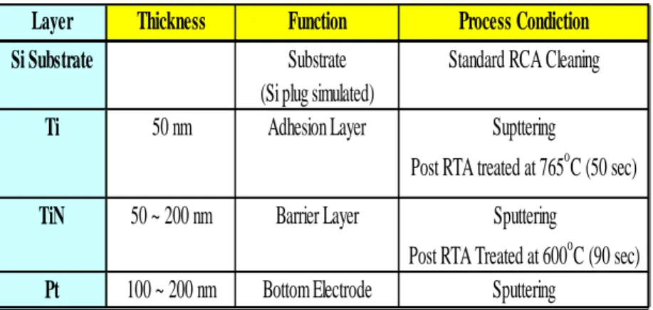
Table 1-1 DRAM device requirements and overall technology trend. Table 1-2 Comparisons of the relevant properties for various dielectrics.
Table 1-3 Comparisons of various technologies for BST films deposited at different conditions.
Table 1-4 Comparisons of various post treatment technologies. Table 2-1 The solution roadmap of DRAM capacitor.
Table 2-2 Bottom electrode requirements for stacked BST capacitor. Table 2-3 Different excimer laser gases and corresponding wavelengths. Table 3-1 The process parameters of Pt/TiN/Ti/Si substrate preparation Table 3-2 The process conditions of BST deposition
Table 4-1 The dynamic dielectric constant, static dielectric constants and optical dielectric constants of BST films prepared in various OMR.
Table 7-1 The comparisons of the composition properties between Cr and BST crystals.
Table 8-1 Comparing with various process parameters for the influences on material and electric properties of BST thin film sputtered at low temperature.
Table 8-2 Electric properties of the BST films before/after post treatments using ELA and oxygen plasma techniques.
Table 8-3 Comparisons of the electric properties between BST mono-layer film and BST/nano-scaled Cr/BST multifilm.
Table B-1 FWHM, grain sizes and root mean square roughness (RRMS) of PSrT
films prepared in various conditions.
Table B-2 Remanent polarization (Pr), saturation polarization (Ps) and coercive field (Ec) of PSrT films prepared in various conditions.
Table B-3 Comparisons of dielectric characteristics for the ferroelectric films fabricated from different kinds of material and by various deposition techniques.
Figure Captions
Figure 1-1 The schematic representation of typical COB stacked cell. (1) storage node, (2) storage node junction, (3) cell transistor, (4) world line interconnection, (5) metal or silicide plug and (6) metallized interconnection and dielectric isolation layers [2].
Figure 1-2 Comparisons of N/O, Ta2O5 and BST performance [22].
Figure 2-1 Figure 2-1 (a) Schematic diagram of 1T1C-transistor cell in DRAMs. (b) Operation scheme and stress bias conditions [35].
Figure 2-2 Schematic cross section of (a) stacted and (b) trench capacitor cell [7]. Figure 2-3 The schematic representation of the stacked cell using the typical
structure of capacitor under bit-line (CUB) [3]
Figure 2-4 The evolvement trend of the multilayer structure used for DRAM cell capacitors.
Figure 2-5 DRAM capacity requirement for (a) average Mbytes/system by computer segment, and (b)major application demand [38].
Figure 2-6 Historical and future trends of (a) lithographic resolution capability, (b) estimation of cell sizes and chip sizes of gigabit density based on the 8F2 folded bit line. (c) The maximum stack height of cylinder-type COB stack cell [4, 5, 39].
Figure 2-7 (a)Trend of the channel length and the substrate doping density of the cell transistor as a function of memory density. (b)Min cell capacitance
as a function of substrate doping density. (c) Data retention time as a function of DRAM density [4, 6].
Figure 2.8 Trend of dielectric materials applied on various DRAM generations [40]. Figure 2-9 The dispersion relation of dielectric constant and tangent loss of the
dielectric materials [41].
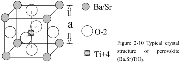
Figure 2-10 Typical crystal structure of perovskite (Ba.Sr)TiO3. Figure 2-11 Various phase transitions in barium titanate.
Figure 2-12 Temperature dependence of the spontaneous polarization and permittivity in s ferroelectric material.
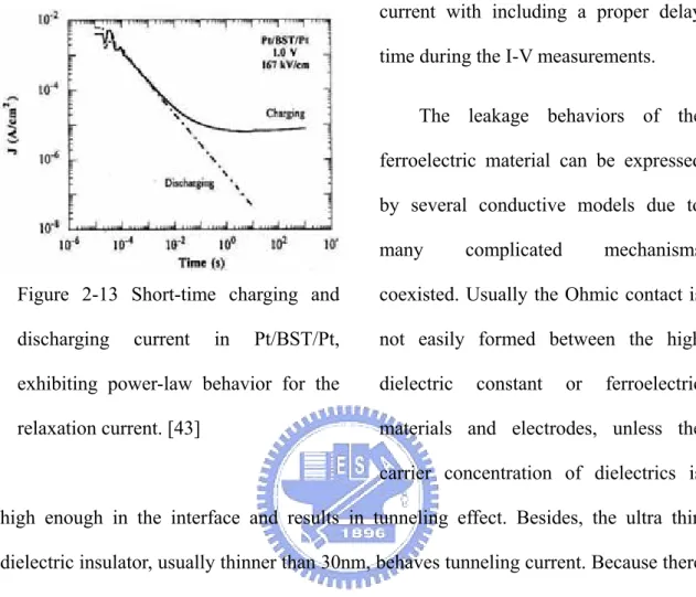
Figure 2-13 Short-time charging and discharging current in Pt/BST/Pt, exhibiting power-law behavior for the relaxation current [43].
Figure 2-14 The circuit model of tangent loss due to the leakage current through the loss by a parallel resistance.
Figure 2-15 Equivalent circuit for a capacitor in series with a high resistance electrode. Cd, Re, Ce and Re stand for the capacitance and resistance of the dielectric and those of the electrode, respectively [43].
Figure 2-16 Schematic graphs of the frequency dependence of Cs and D. Cs and D show the Debye-type dispersion [25].
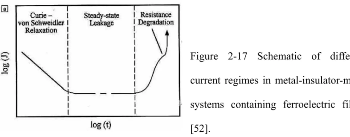
Figure 2-17 Schematic of different current regimes in metal-insulator-metal systems containing ferroelectric films [52].
Figure 2-18 Average grain size of laser crystallized poly crystalline silicon films as a function of the laser energy fluence [72].
Figure 2-19 Time dependence of Si-layer melt front profiles under excimer laser irradiation [85].
Figure 2-20 The transition of grain size distribution using various numbers of shots to perform excimer laser annealing [75].
Figure 3-1 The experimental concepts of this thesis.
Figure 3-2 The experimental flow of the processes and the analysis for the BST capacitor formation.
Figure 3-3 The experimental flow of the processes and the analysis for the ELA treatments.
Figure 3-4 Fabrication process of the thermal testing capacitor with intercrossing electrodes.
Figure 3-5 The schematic diagram of the RF magnetron co-sputter system.
Figure 3-6 The (a) The four-level energy system (KrF excimer laser) scheme and (b) ELA system.
Figure 3-7 The schematic diagram of the MIM testing sample with TiN/Ti barrier layers.
Figure 3-8 Block diagram of the Keithley C-V package 82 system.
Figure 3-9 The typical hysteresis loop of the P-E curve in ferroelectric state. Figure 4-1 Cross-sectional micrograph of BST/Pt/TiN/Ti/Si capacitor.
Figure 4-2 Deposition rate of (a) BST films, (b) individual STO and BTO films versus OMR with sputtering power 230W/175W applied on STO/BTO targets respectively.
Figure 4-3 The plasma spectra of (a) Sr plasma in pure Ar ambient, (b) Sr plasma in 2.5% OMR, (c) Ar plasma in pure Ar ambient and (d) Ar plasma in 2.5 % OMR, all detected near SrTiO3 target.
Figure 4-4 The Ba/Ba+Sr ratio of BST films prepared in various OMR.
Figure 4-5 XRD patterns of BST films deposited on Pt/TiN/Ti/Si substrates with various OMR.
Figure 4-6 AES spectra of BST films sputtered in (a) 5% and (b) 25% OMR.
Figure 4-7 (a) Grain sizes and relative XRD intensities of (100) and (110) textures for the BST films sputtered at various OMR; (b) Dielectric constant of BST films prepared at various OMR.
Figure 4-8 AFM images of BST films deposited in (a) 0% OMR (RRMS = 5.06 nm) and (b) 12.5% OMR (RRMS = 2.46 nm).
Figure 4-9 (a) Leakage current density, (b) tangent loss, and (c) the time-zero dielectric breakdown (TZDB) field of Pt/BST/Pt capacitors prepared in various OMR.
Figure 4-10 TDDB as a function of electric field of BST films deposited in various O2/Ar+O2 ratio (OMR).
Figure 4-11 (a) The log (J/T2) versus E1/2 plot showing Schottky emission fitting, and (b) the log (J/E) versus E1/2 plot showing Poole-Frenkel emission fitting for BST films prepared in various OMR.
Figure 4-12 (a) the range of applied field for SE/PF mechanism in various OMR ambient, and the diagrams of the electron energy band in (b) pure Ar or lower OMR ambient and (c) higher OMR ambient.
Figure 5-1 The reflectivity, R, and the extinction coefficient, k, of amorphous thin Ba0.5Sr0.5TiO3 film for light of wavelength from 198 nm to 900 nm. Figure 5-2 The process schemes of ELA treatment applied on the
BST/metal-bottom-electrode multilayer: (a) during ELA process and (b) after ELA treatment.
Figure 5-3 Cross-sectional TEM micrographs (a) bright-field images for the KrF-excimer-laser annealed PZT films, and (b) SADP of upper layer region and (c) lower layer region of PZT thin film [134].
Figure 5-4 The XRD patterns of thin BST films (a) as-deposited, (b) with 300oC PA, (c) with 46.7 mJ/(cm2×pulse) ELA, (d) with 57.8 mJ/(cm2×pulse) ELA, and (e) with 66.7 mJ/(cm2×pulse) ELA.
Figure 5-5 The fractional intensity of the (111) texture for the BST film post treated at various condition.
Figure 5-6 TEM diffraction patterns of (a) PA 300oC in O2 ambient only, (b) 46.7 mJ/(cm2*pulse) ELA treated BST films
Figure 5-7 Polarization versus electric field of BST film treated at various ELA conditions.
Figure 5-8 (a) The dielectric constants and equivalent SiO2 thickness of the BST films versus LEF, and (b) the dielectric constant versus the thickness of the as-deposited/the 57.8 mJ and the (cm2×pulse)-ELA-treated BST film. Figure 5-9 (a) Leakage current density and tangent loss of the Pt/BST/Pt capacitors post treated at various ELA conditions, and (b) the leakage current
density versus the thickness of as-deposited and the 57.8 mJ/(cm2× pulse)-ELA-treated BST film.
Figure 5-10 The TDDB reliability of BST films treated at various conditions.
Figure 5-11 The leakage current densities of the Pt/BST/Pt/TiN/Ti capacitors biased at positive/negative voltage with various treatments.
Figure 5-12 Oxygen species in-situ detected by RGA during ELA process.
Figure 5-13 The electron energy band of (a) as-deposited BST film biased at positive voltage, (b) BST film post annealed in O2 and biased at negative voltage, and (c) ELA-BST film biased at negative voltage.
Figure 6-1 The typical curve of the leakage current versus the electric field for the as-deposited BST films.
Figure 6-2 Dependence of the the leakage current measured at various electric fields with a delay time of 30 s on duration of O2 plasma treatment after BST film deposition.
Figure 6-3 The surface roughness of (a) as-deposited BST thin films and (b) 5-min O2-plasma-treated BST film.
Figure 6-4 X-ray diffraction patterns of BST thin films with O2 plasma treatment for different durations after BST film deposition.
Figure 6-5 The dielectric constant and the estimated grain size versus the duration of O2 plasma treatment on the BST films.
Figure 6-6 AES profiles of the BST films post treated by oxygen plasma under various treatment durations.
films.
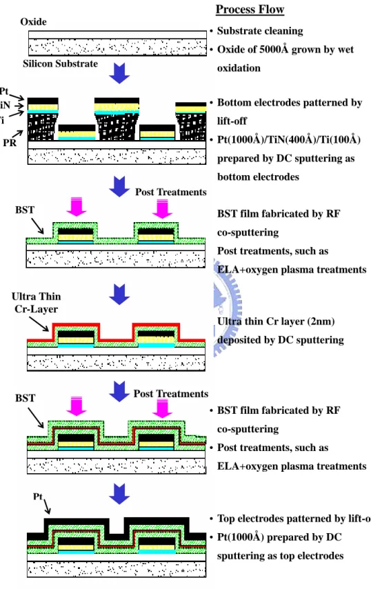
Figure 7-1 (a) The testing structure of Pt/BST/Pt/TiN/Ti multifilm with intercrossing top/bottom electrodes, and (b) the top view photograph of this intercrossing structure.
Figure 7-2 Fabrication process of the BST capacitor with intercrossing electrodes Figure 7-3 The leakage current versus Cr-thickness for the BST/nano-scaled Cr/BST
under electric field of 125 KV/cm at various temperatures.
Figure 7-4 ((a) Capacitance versus temperature with different Cr thickness and (b) Temperature Coefficient of Capacitance (TCC) of the BST/nano-scaled-Cr/BST multifilms measured from 30oC to 150oC.
Figure 7-5 a) The dispersion relation of tangent loss and (b) the tangent-loss for the mono BST layers (400nm) and the BST/nano-scaled-Cr/BST (200nm/2nm/200nm) at various temperatures.
Figure 7-6 XRD patterns of BST/nano-scaled-Cr/BST thin films with various Cr thicknesses.
Figure 7-7 The cross sectional TEM pictures for the structures of (a) BST/Cr(2nm)/BST and (b) BST/Cr(3nm)/BST.
Figure 7-8 The EDS results of (a) Cr layer of BST/Cr(2nm)/BST (b) ”discontinuous region” of BST/Cr(2nm)/BST and (c) any region at BST/Cr interface of BST/Cr(3nm)/BST.
Figure A-1 The testing structure of Pt/BST/Pt/TiN/Ti multifilm with intercrossing top/bottom electrodes.
Figure A-2: The resistances and the TCR of the BST films polarized at –3 volts for the films (a) without RTA and with RTA treatment at (b) 500oC and (c) 600oC.
Figure A-3 The log (J/T2) versus (a) E1/2 and (b) 1/T plots showing Schottky emission fitting for the BST films treated with various RTA conditions at negative bias.
Figure A-4 The resistances and the TCR of the BST films polarized at +3 volts for the films (a) without RTA and with RTA treatment at (b) 500oC and (c) 600oC.
Figure A-5 The log (J/T2) versus 1/T plot showing Schottky emission fitting for the BST films with various RTA conditions at positive bias.
Figure A-6 The electron energy bands for the RTA-treated BST films biased at (a) negative and (b) positive voltages.
Figure B-1 XRD patterns of PSrT films deposited onto Pt/SiO2/Si substrates (a) at
various laser energy fluence, and (b) at various
2
O
P .
Figure B-2 The fractional intensity of (110) orientated texture for the PSrT films deposited at (a) various LEF and
2
O
P 75 mtorr, and at (b) various
2
O
P
and 1.55 J/(cm2*pulse).
Figure B-3 Surface-morphology micrographs of FESEM for the PSrT films deposited at LEF of (a) 1.02, (b) 1.15, (c) 1.55 and (d) 1.70 J/(cm2*pulse).
(b)1.15, (c)1.55 and (d) 1.70 J/(cm2*pulse).
Figure B-5 P-E hysteresis loops of PSrT films fabricated at LEF of (a) 1.02, (b) 1.15, (c) 1.55 and 1.55 (d) 1.70 J/(cm2*pulse) and fixed
2
O
P 75 mtorr, and at
2
O
P of (e) 100 mtorr, (f) 200 mtorr and fixed 1.55 J/(cm2*pulse).
Figure B-6 Capacitance versus applied voltage for PSrT films deposited at various LEF and
2
O
P ( → -5V to +5V, ← +5V to –5V).
Figure B-7 Leakage current density versus applied electric field for PSrT films deposited at various (a) LEF and (b)
2
O
P .
Figure B-8 (a) the dielectric constant and leakage current density (at 100 kV/cm), and (b) the tangent loss for the PSrT films deposited at various LEF. Figure B-9 (a) the dielectric constant and leakage current density (at 100 kV/cm),
and (b) the tangent loss of the PSrT films deposited at various
2
O
Chapter 1
Introduction
1-1 Challenges of Advanced BST Cell Capacitors
1-1.1 BST capacitors applied on advanced DRAM cells
Since the dynamic random access memory (DRAM) with one-transistor and one-capacitor (1T1C) cell was invented in the late 1960s [1], the DRAM technology has progressed at a rapid pace in the past decades. In the past 20 years, the chip density has been quadrupled every three years, and the chip size is 1.5X bigger than that of previous generation. Therefore, three-dimensional (3-D) cell structure has been widely introduced into high-density DRAM cells, and Figure 1-1 shows a typical 3-D cell with capacitor-over-bit line (COB) structure [2].
The stacked cell with COB structure can easily integrate with non-silicon-dioxide
Figure 1-1 The schematic representation of typical COB stacked cell. (1) storage node, (2) storage node junction, (3) cell transistor, (4) world line interconnection, (5) metal or silicide plug and (6) metallized interconnection and dielectric isolation layers [2].
materials and provide large capacitor area, but there are still many critical requirements for the capacitor scaling down, as listed below [3].
(1) Sufficient capacitance for cell operation: Both of increasing cell area and using high-dielectric materials can enhance the cell capacitance. However, the planar dimensions of capacitors and stacked height must be severely constricted due to cell size shrunk of new generation requirements [4, 5]. Therefore, the high dielectric materials must be necessary for advanced capacitor applications.
(2) Low leakage-current/dielectric ratio for data retention: The data retention time is one of the most important parameters for DRAMs’ applications. The data retention time is the period of the stored data lost owing to the leakage current before data refreshing, and that has to be doubled as the memory density increases 4X in every new generation [6]. Therefore, the node leakage must be improved to obtain a better data retention property.
(3) Plenty of manufacturing resources and mature technologies for CMOS-IC processes:
DRAM Generation Lithography (µm) Cell Area (µm2) Device Voltage (V) Cell Capacitance (fF) Equivalent Oxide Thickness, tox (nm) Maximum Capacitor Voltage, VBLH, VWLL=0 (V) 1Mbit 1.00 30.00 5.0 35-40 8.8 2.7 4Mbit 0.80 10.00 5.0 35 8.8 2.7 16Mbit 0.50 3.50 3.3 30-35 6.6 1.8 64Mbit 0.35 1.30 3.3 30 6.6 1.8 128Mbit 0.25 0.75 2.5 25-30 5.0 1.2 256Mbit 0.18 0.25 2.5 25 5.0 1.2 512M~1G bit 0.13 0.11 1.8 25 3.6 0.7 4Gbit 0.10 0.07 1.5 >25 3.0 0.4 16Gbit 0.07 0.03 1.2 >25 2.4 0.3 32Gbit 0.045 0.012 1.0 >25 2.0 0.25
In practical applications, cost and production feasibilities are the key concerns for the developments of new generation technologies. The mature techniques, such as CVD and PVD, used for thin film fabrications can easily satisfy those targets of the cost reduction and the feasibility concerns. Especially, the fabrication cost will be incredibly huge for the generation scaled down to nano-order, so plenty of manufacturing resources will become very high priority for the new technology developments.
(4) Performing excellent reliability to satisfy the qualification criteria in practical
applications: The qualification criteria become more and more severe for new
generation IC chip due to the crucial requirements in high-speed, low power and embedded memory integrated into a system-on-chip (SOC). For instance, according to the industrial standards, the operation junction-temperatures for DRAMs’ applications and qualification spec range from –0 oC to 120oC (ambient temperature ranging from –40~85 oC for consumer IC), so the thermal stabilities of the electrical properties become the very critical concerns for the device developments and
Medium dielectric constant materials
Dielectric εr Ccrit (fF µm -2 ) Note SiO2 3.9 25 Si3N4 7 7 ~ 10 Ta2O5 25 ~ 50 12 ~ 20 TiO2 30 ~ 40 10 ZrO2 14 ~ 30 10 Nb2O3 30 ~ 100 -Y2O3 15 ~ 20 5
(Ba, Sr)TiO3 (BST) 300 ~ 800 40 ~ 120 Paraelectric Phase
(Pb, La)(ZrTi)O3 (PLZT) ~1400 80 ~ 90 Ferroelectric Phase
applications.
The requirements of the DRAMs’ cells from 1Mbit to 64Gbit are summarized in Table 1-1, which was further modified by the information of ITRS 2003 and IBM Res. [7, 8]. This technology roadmap reveals the high dielectric materials applied on cell capacitor is indeed necessary for giga-bit generation DRAM.
(Ba, Sr)TiO3 (BST) film has been investigated as capacitor’s material for giga-bit
DRAM applications because of the following reasons.
(1) Extremely large dielectric constant: BST has a very large dielectric constant at the high frequency zone for memory operation. Comparing with many high-k dielectrics, BST exhibits unbelievably high dielectric constant in paraelectric phase, as depicted in Table 1-2 [9~11]
(2) Lower leakage-current/dielectric ratio for data retention: BST capacitor behaves semi-insulation properties, but the leakage current is still acceptable during refreshing cycle. Figure 1-2 shows the effective oxide thickness versus leakage
Figure 1-2 Comparisons of N/O, Ta2O5 and BST performance [22].
current using different high dielectric materials, such as N/O, Ta2O5 and BST [22].
Obviously, the effective oxide thickness of the BST is smallest at the same leakage current, that is, BST has best capability for charge storage among such high-k materials. Hence, the BST capacitor possesses excellent property of data retention. (3) Compatible materials for CMOS processing: The film does not contain the harmful
elements, such as Na, K and Li, which can greatly degrade the performance of Si transistor.
(4) Paraelectric phase in operation temperature: The composition of BST film can be adjusted into paraelectric phase, without spontaneous polarization, at operation temperature, so the film can get rid of fatigue phenomenon.
(5) Plenty of fabrication resources: Abundant technologies can be easily applied on this film fabrication, such as sputtering, sol-gel, PLD, CVD etc., so it’s easy to find a suitable resource to reduce the cost.
Consequently, according to the above excellent characteristics, BST thin film capacitors are almost able to satisfy the requirements of the new generation cell capacitors, but some of the integration obstacles must be concerned below.
1-1.2 Challenges of BST capacitors integrated with CMOS IC
processing
BST is the best candidate of Giga-bit DRAM material, but there are still some challenges for the integrations of CMOS processing.
(1) CMOS devices deformed by high temperature process: In general, high temperature (>450oC) deposition of BST films is frequently applied to obtain good crystallinity of a perovskite structure [12, 13], as denoted in Table 1-3 [23 - 34], but the high temperature process may deform the junction profile and alter the gate length of the metal-oxide-semiconductor field-emission-transistor (MOS-FET), especially on the deep submicron scale. In stacked-capacitor (STC) structure, the MOS-FET dopant is always implemented prior to the capacitor fabricated, which needs to be fabricated at low temperature to avoid the damage of the MOS-FET.
(2) Difficult electrode formation of BST capacitor: Usually, there is serious inter-diffusion between dielectrics and silicon during the deposition of dielectrics. A thermally and electrically stable diffusion barrier is needed to prevent inter-diffusion,
Table 1-3 Comparisons of various technologies for BST films deposited at different conditions.
Deposition Technologies Post Treatments
Low Temperature
Process Anounced?
Compositions Substrates Film Thickness (nm)
Dielectric Constant Reference
RF-sputtering (660oC) n/p no (Ba0.75, Sr0.25)TiO3 Pt/SiO2/Si 30 250 [23]
RF-sputtering (640~660oC) n/p no (Ba0.5, Sr0.5)TiO3 Pt/SiO2/Si 20 320 [24]
RF-sputtering (500~550oC) n/p yes (Ba0.4, Sr0.6)TiO3 LNO/Pt/Ti/SiO2/Si 80 250 [25]
ECR-sputtering (200oC) Microwave (300oC) *1 yes SrTiO3 Pt/Ti/SiO2/Si 200 260 [26]
CVD (400oC) Furnace Annealing (700oC) yes (Ba0.6, Sr0.4)TiO3 Pt/TaOx/SiO2/Si 30 170 [27]
CVD (400oC) Furnace Annealing (600oC) yes (Ba0.6, Sr0.4)TiO3 SRO 10 < 260 [28]
LSCVD (500oC) n/p no (Ba0.5, Sr0.5)TiO3 Pt/Poly-Si/SiO2 35~200 300 [29]
ECR-CVD (450oC) RTA (700oC) yes (Ba0.5, Sr0.5)TiO3 Pt/TaOx/Si 61 220 [30]
Sol-gel (RT) Furnace Annealing (700oC) no (Ba0.5, Sr0.5)TiO3 Si 250 435 [31]
MOD (RT) Furnace Annealing (750oC) no (Ba0.7, Sr0.3)TiO3 Pt/Ti/Si 140 480 [32]
PLD (700oC) *2 n/p no (Ba0.6, Sr0.4)TiO3 Pt/Ti/SiO2/Si 200~400 450~600 [33]
PLD (400oC) *2 ELA(400oC) yes BaTiO3 Pt/Ti/Si 250 150~1200 [34]
BST samples prepared by various techniques
*1: Microwave treatment behaves low substrate temperature, but high thermal budget. Besides, this technique may damage the underlayer due to bump heating. *2: PLD technology behaves bad uniformity for practical applications.
and it also cannot be oxidized during high temperature processes with O2 ambient.
(3) Leakage current increasing after thermal cycles or Ar/N2 plasma processing: The
leakage current of the BST film would be greatly increased after post annealing or ion sputtering process [1.14~1.17]. Although the dielectric properties can be greatly enhanced, the increased leakage current will result in the degradation of the data retention.
(4) Dramatic variations of the dielectric properties for the device operating in various
temperatures: The dielectric constant and the conduction current can decrease about
20% and increase 3-order, respectively, while the BST capacitor operates from room temperature to 110oC [18,19]. In industrial criteria, the operation junction-temperatures for DRAMs’ applications and qualification spec range from –0 oC to 120oC (ambient temperature ranging from –40~85 oC for consumer IC), so the dramatic variations of the electric-temperature properties may cause the deviation of the normal device operation.
Therefore, the thin film technologies of the BST capacitors must overcome the above tough barriers, or it should be impossible to perform the practical DRAM applications.
1-2 Motivation of this Thesis
This thesis dedicated in obtaining excellent characteristics of BST capacitor fabricated by low-temperature novel technologies. The motivation and the major concepts of this study are listed below.
(1) Optimizing the process controls for BST thin film fabricated at low temperature: In general, Dual-Gun RF-sputtering-system can reduce the reaction energy than Single-Gun RF-sputtering-system theoretically, so this sputtering technique was applied on BST film fabrication in this thesis, using two individual targets, BaTiO3
and SrTiO3, simultaneously. Although a low temperature technique is required for
the deposition of BST in the IC process, controlling the crystallinity and dielectric constant is normally more difficult with a low temperature technique than with a high temperature technique. The process parameters and the electrical mechanisms were systematically studied to obtain the optimal process conditions.
(2) Enhancing the crystallinity of BST films using the novel post-treatment of ELA
technique: Low temperature prepared BST films always exhibit poor crystallinity,
so the films have to be post treated by the annealing process to enhance the crystallinity and dielectric properties. A novel low-temperature technique, using excimer laser annealing (ELA), was introduced in this work due to its very low thermal budget and high crystallization efficiency. In addition, the shallow depth of energy absorption using ELA won’t damage the under layer devices. Hence, ELA is an extremely powerful technology to achieve a successful integration process at low temperature. The comparisons of several post treatment technologies are listed in Table 1-4, which shows ELA possesses excellent characteristics for thin film applications. Although ELA technology is widely used for preparing poly-Si thin film in current semiconductor industry, but up to now, very few reports investigate the ELA mechanism for ferroelectric films. Hence, this thesis investigated the effects, the mechanisms and the process window of ELA technique applied on BST
films.
(3) Suppressing the leakage current using oxygen plasma technique after post annealing: The leakage current increases after sputtering and post annealing process due to surface damage. Oxygen plasma treatment can effectively improve the surface states, and therefore the leakage current can be greatly reduced because of oxygen vacancies compensation.
(4) Enhancing thermal stability using the novel sandwich structure of BST/Nano-scaled
Cr/BST Multifilm: The stable properties of the dielectric constant and conducting
current are indeed necessary during device operating. The nano-scaled Cr layer was applied onto the BST capacitor to enhance the thermal stability. The electric characteristics and corresponding mechanisms will be systematically discussed in this investigation.
Besides, according to previous studies, the excellent bottom electrodes can be obtained by the formation controls of the Pt/TiN/Ti/Si multilayer films, and the barrier capability of the TiN layer can be largely enhanced by rapid thermal annealing (RTA)
Thermal Budget Mechanical
Stress Releasing Uniformity
Throughput for Mass Production
RTA low bad good good
Microwave high good excellent good
Furnace Annealing high excellent good excellent
ELA with Optical
Scanning System low excellent good worse *
Comparisons of Various Post Treatment Technologies
* The throughput of ELA technique can be improved by equipment modifications
[14, 20, 21]. Therefore, this thesis won’t discuss the electrode formation anymore.
1-3 Thesis Organization
This thesis reports how the novel low temperature techniques applied on the BST capacitor fabrications. The structure of Pt/TiN/Ti/Si was proposed as the bottom electrode substrate for BST deposition, simulating the COB capacitor structure of DRAM capacitor in this study. Electrical and material properties are systematically analyzed in this work.
Chapter 2 reports the general background and the literature review of BST thin film capacitors. Lots of works reported the DRAM’s new generation trends and developments, low-temperature techniques, mechanisms/applications of BST thin films, obstacles and potential solutions for BST applications.
Chapter 3 presents the details of the experimental concepts and the equipments of this study. The experimental procedures, thin film fabrication processes, electric and material analysis techniques will be introduced in this chapter.
Chapter 4 investigated the characteristics of the low-temperature prepared BST Films. Processing parameters were carefully controlled and studied, and then the experimental results show oxygen/argon-mixing-ration (OMR) plays a most important role in the RF co-sputtering process. The corresponding analysis of the electric and the material properties were performed in this chapter.
Chapter 5 demonstrates the effects of ELA treatment applied on the BST capacitors. The mechanisms of recrystallization were thoroughly analyzed by thermal conduction analysis. Furthermore, the material and the electric analysis show the process window
of the ELA BST film is very hard to control. This chapter thoroughly investigated the ELA processing issues.
Chapter 6 presents the post treatment using oxygen plasma applied on the BST/Pt/TiN/Ti/Si multilayer films. The great enhancement of leakage suppressing can be achieved, and the corresponding mechanisms were studied.
Chapter 7 demonstrates a novel sandwich structure of BST/nano-scaled-Cr/BST multifilm was introduced into the cell capacitor. The thermal stability of BST capacitance can be greatly enhanced by applying this nono-scaled Cr layer. The electric characteristics and corresponding mechanisms will be systematically discussed in this investigation.
Chapter 2
General Backgrounds and Literature
Review
2-1 General Backgrounds of DRAM Cell
2-1.1 Overview on DRAM Cell
Figure 2-1(a) shows a DRAM cell with one-transistor and one-capacitor (1T1C) structure, and Fig. 2-1(b) depicts one of the typical cell operations [35]. The cell data is read out to bit line (BL) while the selected world line (WL) is boosted to Vpp. After
sensing, the BL voltage is fully amplified to internal array operation voltage Vaa for data
“1” and Vss for data “0” simultaneously. For data “1” write, the WL voltage must be
higher than Vpp (=Vaa+Vtcell) to write data “1” to the memory cell, where Vtcell is the
threshold voltage of the cell transistor. Besides, for data “0” write, the bit line must be biased to ground.
In the early age of DRAM development, two-dimensional cell structure, formed by double polysilicon transistor, was widely applied on the standard DRAM cell, known as the “planar type” DRAM. Three-dimensional cell structure was introduced to 4Mb-above generation, and these innovations included the trench capacitor cell and stacked capacitor cell (STC). Both of the trench and the stacked cell techniques are used
in commercial DRAM products till now, but they have been greatly improved in the past generations, as depicted in Figs. 2-2 (a) and (b) [36, 37]. The most important benefits of the trench cell are high transistor performance and effective topology. Excellent transistor performance results from the trench capacitor formed at the early processing stage, so the thermal budget can be reduced during chip fabrication. Hence, it makes trench technology more favorable as the embedded memories integrated with the high performance CMOS logic [7]. The topology of trench can effectively raises the capacitance up, but without increasing the planar cell area. The disadvantages of trench cell come from the obstacles of the manufacture and the new material applications. The extremely deep trench etching and the cell isolation are very difficult to be manufactured by semiconductor processing technologies. In addition, the leakage current density of the trench capacitor rapidly increases as the cell size decreases due to lots of profile defects. Trench cell also lacks of fabrication technologies for high dielectric material applications, such as penta-oxide (Ta2O5) and barium strontium
Figure 2-1 (a) Schematic diagram of 1T1C-transistor cell in DRAMs. (b) Operation scheme and stress bias conditions [35].
World Line (Row) Bit Line (Column) VBB Read/Write Select Read/Write Data Cell Node Storage Capacitor Cell Plate
(b)
(a)
titanate (BST).
On the other hands, the benefits of using the stacked cell (STC) are that the standard techniques of the planar silicon processing are still available for this capacitor fabrication, which is contained in the multiple interconnect layers above the silicon. Therefore, lots of techniques can be applied on the stacked capacitor using the high dielectric materials. Stacked cell has been changed from the capacitor-under-bit line (CUB) to capacitor over bit line (COB) structure to increase the cell capacitance, as shown in Figs. 2-3 and 1-1 respectively. Compared with CUB, the COB stacked cell can
Figure 2-2 Schematic cross section of (a) stacked and (b) trench capacitor cell [7].
Figure 2-3 The schematic representation of the stacked cell using the typical structure of capacitor under bit-line (CUB) [3].
(b)
(a)
provide larger cell area, so that will be a promised candidate for the giga-bit scaled DRAM. Although COB could be able to applied on giga-bit generation, there are still many challenges for scaling down, such as large leakage current at the storage junction, variation of cell transistors’ threshold voltage, parasitic resistance and capacitance between the bit-line/the cell-capacitor, and insufficient cell area. However, insufficient cell area is one of the most disadvantages for STC, so the high dielectric material is indeed necessary as the capacitor material for the new generation stacked-cell [3].
Memory cell capacitance plays a key role, which can determine the sensing signal margin, speed, data retention time and endurance against the soft error. In the multimega bit generation, the minimum cell capacitance should be 25 fF/cell. Capacitance can be described as the following equation.
d A CS ε × = (2-1)
where CS is the memory cell capacitance, εis the capacitor dielectric, A denotes the
capacitor area and d is the capacitor thickness. The leakage current at the cell node, consisted by sub-threshold leakage, irradiation charge loss, noise coupling, junction leakage and cell dielectric leakage, will strongly affect the sensing signal margin, as shown in the following equation.
) ) (( ) ( 1 ) ( 2 1 C N B ref d sub j B S cc S B S s I I I t C V Q C C V C C C V + + + + + − + = (2-2)
where VS presents the sensing signal voltage, CB is the parasitic bit line capacitance, Ij,
Isub and Id indicate the current of junction leakage, sub-threshold leakage and dielectric
transistor-threshold/sensing amplifier mismatch, and QC is the charge loss induced by
irradiation [2]. To obtain the excellent properties of crystallinity and leakage reduction, the choice of electrode structure is another important concern. The trend of electrode-capacitor material structure is shown in Fig 2-4. The capacitor of COB cell adopted the silicon-insulator-silicon (SIS) structure before, but the novel Ta2O5 or Al2O3
dielectric in metal-insulator-silicon (MIS) is replacing the long-lived NO dielectric in SIS, ranging from 0.18μm to 100 nm node. As the feature size shrinking under 100 nm, the advanced high-K dielectric, Ex. BST, with metal-insulator-metal (MIM) will be inevitably applied on the giga-bit generation DRAM cell.
Ox or NO Poly Silicon Poly Silicon Ta2O5 or Al2O3 Metal Poly Silicon High-K Dielectric (BST) Nobel Metal Nobel Metal Barrier & Adhesion Layer
SIS
MIS
MIM
0.18um above 0.18um ~ 100nm New GenerationFigure 2-4 The evolvement trend of the multilayer structure used for DRAM cell capacitors.
2-1.2 Trend and Challenges of DRAM
In the past 20 years, the desktop PC was the primary driver for DRAM’s industry. Although the PC market still keeps on growing, the DRAMs’ market structure must be modulated due to the high-end demand rising [38]. Fig. 2-5(a) indicates the memory sizes for the computer segment. In general, the communication servers require the highest density DRAM in each generation. Fig. 2-5(b) presents the
market trends of 128-megabit-equivalent DRAM. Obviously, the market share of PCs’ DRAM are decreasing, but that of communications’ is greatly growing. The evolution of CMOS technologies was described as Moor’s law, which predicted the number of components would be double on the integrated circuit (IC) chip each year. The common rule of Moor’s law is still useful even though that has been modified several times [39]. The trend of lithographic capability was predicted by Semiconductor Figure 2-5 DRAM capacity requirement for
(a) average Mbytes/system by computer segment, and (b)major application demands [38]. Desktops Communication
(b)
Servers Workstations Notebook Desktop Sub-portables(a)
Industry Association (SIA), as shown in Fig. 2-6(a), where half pitch is the minimum size of lithographic features on a chip. According to the experiential rule in the past 20 years, the chip density has been quadrupled every three years, and the chip size is 1.5X bigger than that of previous generation. In addition, the chip speed keeps on improving in spite of the chip size increasing. Table 1-1 shows the DRAM device requirements and overall technology trend. Fig. 2-6(b) shows the forecast of the chip-size/cell-size versus generation, based on the architecture of 8F2 folded line cell, where F is the feature size [4]. The vertical stack height is another important factor of COB technologies. To meet the requirement of minimum cell capacitance, dielectric thickness decreasing or stack height increasing are carried out as the solutions of the new generation cell, but both of them will induce large leakage current. The upper limitation trend of the stack height is shown in Fig. 2-6(c), which shows the stack height must be lower than 1μm to satisfy the 0.11μm technology and under [5].
The DRAM manufacturing was developed from 4Mb to 256Mb through the decade of the 1990s. During those generations, density-enhancing technologies dedicated in the shallow trench isolation (STI), bit-line contact borderless to world-line, capacitance enhancing, junction leakage suppressing and self-aligned buried strap [7]. A high substrate doping density, > 5×10¹⁷ /cm3, was required in order to keep the threshold voltage at 1 volt to suppress the short channel effect, but the junction leakage current would be the crucial issues due to this high doping density. Hence, the self-aligned channel implantation was introduced as the solution of substrate doping suppressed [2, 4]. The trend of cell transistor’s channel length is a function of substrate doping density, as shown in Fig. 2-7(a). In general, the minimum accepted cell capacitance is
Figure 2-6 Historical and future trends of (a) lithographic resolution capability, (b) cell sizes and chip sizes estimations based on the 8F2 folded bit line. (c) the
maximum stack height of cylinder-type COB stack cell [4, 5, 39].
Figure 2-7 (a) Trend of channel length and substrate doping density of cell transistors. (b) Min cell capacitance as a function of substrate doping density. (c) Data retention time as a function of DRAM density [4, 6].
(b)
(a)
(c)
(b)
(a)
(c)
reduced as the new generation progressing, but that must be higher than 25 fF /cell for the giga-bit DRAM cell. High doping density results in the junction leakage current increasing, so the cell capacitance must be higher than 25 fF /cell, as shown in Fig. 2-7(b). However, the requirements of the DRAMs’ cells from 1Mbit to 64Gbit are summarized in Table 1-1, which was further modified by the information of ITRS 2003 and IBM Res. [7, 8]. Besides, the data retention time is the one of the most important parameters for DRAMs’ applications. The data retention time is the period of the stored data lost owing to the leakage current before data refreshing. The data retention time has to be doubled as the memory density increases 4X in every new generation to satisfy the requirements of high speed and low power consumption, as shown in Fig. 2-7(c) [6]. The leakage current at a cell node, which was consisted by the cell transistor sub-threshold current, cell dielectric leakage and source/drain junction current, greatly influences the data retention time. Therefore, to obtain a better data retention property, the node leakage should be improved in many ways, such as interface improvement of shallow trench isolation, electric field suppressed at the cell node junction and material improvement in cell dielectric layer.
Year of the First Product Shipment, Technology Node 2001 130 nm 2002 2003 2004 90 nm 2005 2006 2007 65 nm 2010 45 nm 2013 32nm 1016 22nm Upper Electrode
High-k Dielectric ONO or NO Bottom Electrode
Metal
Poly Silicon Metal Perovskite
Ta2O5, Al2O3 BST, STO Epi BST
The selections of dielectric material and the electrode structure are very important for the electric properties of cell capacitor. Fig. 2-8 depicts the roadmap of capacitors’ material applied on various DRAMs’ generations [40]. The cell capacitor of the high density DRAM adopted
Si3N4/SiO2 (nitride/oxide, NO) as its
insulator’s material under 256M-bit generation. Because the ultimate of NO dielectric is limited to around 4-nm in oxide equivalent thickness, the only possible solution is to increase surface area using hemi-spherical grain (HSG) technique. However, there is not much room for the cell size scaling down owing to the limitations of the stack height and the HSG grain size. Therefore, a tantalum pentoxide (Ta2O5) is
being applied on the generations of 256M-bit~4G-bit generation now instead of nitride material. The capacitor using Ta2O5 dielectric is based on metal-insulator-silicon (MIS)
structure, but the capacitor structure will switch to metal-insulator-metal (MIM) structure for the generation scaling down to 0.13μm. The metal storage node instead of the poly silicon node is in order to eliminating the native oxide formed at the poly silicon node, but the technique of the metal electrode integrated with Ta2O5 dielectric is
a big challenge due to large leakage current. So far, the Ta2O5 can be further scaled
down to 0.13μm technology, but its limitation will be 2-3 nm in oxide equivalent Figure 2-8 Trend of dielectric materials
applied on various DRAM generations [40].
thickness. One of the prevalent candidate for multi-giga bit generation is probably (Ba, Sr)TiO3 (BST) dielectric, because BST can achieve extremely high dielectric constant
around 150-400 and be crystallized on the noble metal electrode. MIM BST capacitor is the most promised cell capacitor in the near future. Table 2-1 indicates the roadmap of the cell capacitor development using different electrode structures and insulator material.
At current technology timeline, DRAM progressing is limited by further scaling-down of MOSFET channel length, leakage current and insufficient cell capacitance. As DRAM enters the 21st century, the advanced technologies ranging from 0.18μm to below 100nm give bright future for the new generation applications.
2-2 Basic Concepts of the High-k Perovskite Material
2-2.1 The material and the electrical characteristics of perovskite
Ceramic
Capacitor material is one of the most important factors for the characteristic of DRAM cell. Cell capacitance, leakage current and fabrication process can be significantly influenced by this factor. Some of the fundamental parameters of capacitor material are introduced below. The electric displacement D related to polarization P can be expressed as:
D = ε0 E+P = ε0 E+χeε0 E =ε0(1+ χe) E
=ε0εr E = εE (2-3)
where D: electric displacement E: external electric field P: polarization
ε0: the vacuum permittivity
εr: the relative dielectric constant of dielectric material
χe: electric susceptibility E P e ∝∂ /∂ χ (2-3-1) εr=1+χe (2-3-2)
The definition of electric polarization is shown below.
∑
∑
= − = N r N E E P α ε0(ε 1) (2-4) where α is polarizability.The total polarizability can be divided into four possible compositions, as denoted below.
α= αe + αi + αd + αs (2-5)
These four compositions are illustrated as following.
(1) The electronic polarizability, αe, is caused by a slight displacement of the negatively charged electron cloud in an atom relative to the positively charged nucleus. Electronic polarizability occurs in all solids and in some, such as diamond, it is the only contributor to the dielectric constant since ionic, dipolar and space charge
polarizabilities are absent.
(2) The ionic polarizability, αi, arises from a slight relative displacement or separation of anions and cations in a solid. It is the principal source of polarization.
(3) Dipolar polarizability, αd, arises in materials such as HCL or H2O that contain
permanent electric dipoles, these dipoles may change their orientation and they tend to align themselves with an applied electric field. The effect is usually very temperature dependent since the dipoles may be " frozen in " at low temperature. (4) Space charge polarizability, αs, occurs in materials that are not perfect dielectric but
in which some long range charge migration may occurs.
Usually, the polarizability decreases in the order αe < αi < αd < αs. Fig. 2-9 shows
the dispersion relation of dielectric and tangent loss [41]. In general, the tangent is loss due to the leakage current, and that can be express as:
Figure 2-9 The dispersion relation of dielectric constant and tangent loss of the dielectric materials [41].
![Figure 2-3 The schematic representation of the stacked cell using the typical structure of capacitor under bit-line (CUB) [3]](https://thumb-ap.123doks.com/thumbv2/9libinfo/8142119.166716/43.892.146.762.160.426/figure-schematic-representation-stacked-using-typical-structure-capacitor.webp)
![Figure 2-9 The dispersion relation of dielectric constant and tangent loss of the dielectric materials [41]](https://thumb-ap.123doks.com/thumbv2/9libinfo/8142119.166716/53.892.255.625.198.458/figure-dispersion-relation-dielectric-constant-tangent-dielectric-materials.webp)
![Figure 2-19 Time dependence of Si-layer melt front profiles under excimer laser irradiation [85]](https://thumb-ap.123doks.com/thumbv2/9libinfo/8142119.166716/70.892.122.752.159.736/figure-time-dependence-layer-profiles-excimer-laser-irradiation.webp)
![Figure 2-20 The transition of grain size distribution using various numbers of shots to perform excimer laser annealing [75]](https://thumb-ap.123doks.com/thumbv2/9libinfo/8142119.166716/71.892.465.759.169.488/figure-transition-distribution-various-numbers-perform-excimer-annealing.webp)