國 立 交 通 大 學
光電工程研究所
博士論文
以增益開關法布里-珀羅雷射二極體為
基礎的全光通訊信號格式轉換元件研究
All Optical NRZ-to-RZ Format Converter
by a Fabry-Perot Semiconductor Laser
Diode
研 究 生:張詠誠
指導教授:林恭如 教授
以增益開關法布里-珀羅雷射二極體為
基礎的全光通訊信號格式轉換元件研究
All Optical NRZ-to-RZ Format Converter
by a Fabry-Perot Semiconductor Laser
Diode
研 究 生:張詠誠
Student: Yung-Cheng Chang
指導教授:林恭如
Advisor: Gong-Ru Lin
國立交通大學 電機資訊學院
光電工程研究所
博士論文
A Dissertation
Submitted in Partial Fulfillment of the Requirements
for the Degree of Doctor of Philosophy in
The Institute of Electro-Optical Engineering
College of Electrical Engineering and Computer Science
National Chiao-Tung University
Hsin-Chu, Taiwan, R.O.C.
摘 要
論文名稱:以增益開關法布里-珀羅雷射二極體為基礎的全光通訊信號格式轉換元件 研究 校所別:國立交通大學光電工程研究所 頁數:1 頁 畢業時間:九十四學年度第二學期 學位:博士 研究生:張詠誠 指導教授:林恭如 教授 關鍵詞: 法布里-珀羅雷射二極體, NRZ-to-RZ 格式轉換, 光注入鎖定引起的閾值電流 降低現象, 光纖通訊, 全光邏輯或閘, 啁啾 本論文的主旨在利用半導體雷射中光注入鎖定會造成雷射的閾值電流降低現象來實 現一全光式非歸零轉歸零之格式轉換器。閾值電流在注入鎖定半導體雷射情況下所造 成的閾值電流降低現象也做了詳細的理論推導。在實驗上,我們成功地展示全光非歸 零轉歸零的格式轉換器,同時這種利用光注入鎖定的技術可以使法布里-珀羅雷射二 極體同時具備單縱模輸出、啁啾降低與頻寬延展等好處。在應用上,以此種全光格式 轉換器實現之全光或閘也首度被展示。進一步,我們評估輸出歸零光訊號的啁啾特 性,並以日本 NTT 研究群所提出的動態光固子傳輸架構為基礎提出傳輸此格式轉換後 的歸零訊號之傳輸架構。ABSTRACT
Title:All Optical NRZ-to-RZ Format Converter by a Fabry-Perot Semiconductor Laser Diode Pages:1 Page
School:National Chiao Tung University
Department:Institute of Electro-Optical Engineering
Time:June, 2006 Degree:Doctor of Philosophy Researcher:Yung-Cheng Chang Advisor:Prof. Gong-Ru Lin
Keywords : Fabry Perot laser diode, NRZ-to-RZ format conversion, optical injection-locking-induced threshold current reduction, fiber-optic communication, optical OR logic gate, chirp.
In this dissertation, a reduction in the threshold current of a Fabry-Perot laser diode (FPLD) is first used to convert a nonreturn-to-zero (NRZ) to return-to-zero (RZ) formatted data stream. The threshold current reduction in external injection locking condition is derived by using a phenomenological approach to diode lasers and Li’s theory. Such a reduction in the threshold current by the injection locking technique can reduce the linewidth/chirping and enhance the modulation bandwidth of the FPLD. In applications, an NRZ-to-RZ-based all-optical OR logic gate is also demonstrated. Furthermore, by using a spectral windowing, linear dispersion compensation, and a preemphasis technique we believe that a soliton transmission for the RZ-formatted data stream may be expected.
Acknowledgements
博士論文終於完成了。首先要特別對我的指導教授 林恭如老師在研究的過程中 不斷的給予支持與耐心的指導表達敬意與感謝之意,使我在求學態度受益良多。 感謝實驗室歷年學弟士雄、世剴、忠嶸、百勝、鈺晃、銘忠、奕祥、齊冠、家 陽、昆潔與博士班同學俊榮、育聖的陪伴。天下無不散之宴席,我終於要離開這個實 驗室了,期盼接下來的實驗室環境會更好,有更多的研究成果以及積極的研究風氣。 最後我要感謝我最摯愛的家人,尤其是在背後默默支持我的爺爺、爸爸、媽媽、弟弟、 妹妹、叔叔、嬸嬸、姑姑、姑丈等,以及我的女友佩誼及其他關心我的好朋友,對於 你們長期以來的支持與關愛,在此獻上誠摯的感謝。CONTENTS
PageChinese Abstract
IEnglish Abstract
IIAcknowledgements
IIIContents
IVList of Figures
VIIList of Tables
XIIChapter 1
Introduction
1
1.1 Introduction of Semiconductor Lasers 1
1.1.1 Historical Review of Semiconductor Lasers 1
1.1.2 Operating Principles of Semiconductor Lasers 5
p-n Junction 5
Dielectric Waveguide 7
Recombination Mechanisms 8
Laser Threshold 8
1.2 Enabling Technology for Data Format Conversion 10
1.2.1 All-optical Non-Return-to-Zero (NRZ) to Return-to-Zero
(RZ) Data Format Conversion by using Fabry-Perot laser diodes (FPLDs)
11
1.2.2 Techniques for Generating Short Pulse 12
1.2.3 Introduction of Injection Locking 14
1.3 Motivation of an novel FPLD-based NRZ-to-RZ Data
Format Converter
15
1.4 Organization of Dissertation 16
Figures 18
Chapter 2
Theory of Threshold Current Reduction under External Light
Injection Locking
27
2.1 Introduction 27
2.2 A Phenomenological Approach to Diode Lasers 29
2.2.2 Spontaneous Photon Generation in LEDs 33
2.2.3 Photon Generation and Loss in Laser Cavities 36
2.2.4 Threshold or Steady-State Gain in Lasers 39
2.2.5 Threshold Current and Output Power vs. Current 43
2.2.6 Relaxation Resonance and Frequency Response 50
2.3 Threshold Current Reduction Under External Light Injection 55
Table 64 Figures 65
Chapter 3
All-optical NRZ-to-RZ Data Format Converter with An
Injection-locked Fabry-Perot Laser Diode in Unlasing Condition
72
Abstract 72
3.1 Introduction 72
3.2 Operating Principle of Injection-locking-induced
gain-switching in a Synchronously-modulated FPLD just below Threshold Current
73
3.3 Experimental Setup and Results 74
3.3.1 Threshold Current Reduction under External Injection Locking
74
3.3.2 Injection-locking-induced Gain Switching 75
3.3.3 FPLD-based All-optical NRZ-to-PRZ Data Format Converter
78
Table 83 Figures 84
Chapter 4
Injection-locking Laser Diode based OC-192 optical NRZ-to-RZ
OR Logic Gate
100
Abstract 100
4.1 Introduction 100
4.2 FPLD-based All-optical NRZ-to-RZ OR logic gate 101
Figures 104
Chapter 5
Dynamic Chirp Characteristics in FPLD-based All-optical
NRZ-to-RZ Data Format Converter
107
5.1 Introduction 107 5.2 Evaluation of Chirp in FPLD-based NRZ-to-RZ Data Format
Converter
109
5.3 Results and Discussion 111
Table 114 Figures 115
Chapter 6
Conclusions
122 6.1 Summary 1226.2 Suggestions for Future Work 124
References 125 Curriculum Vitae
List of Figures
Fig. 1.1 Schematic illustration of (a) homostructure and (b) double-heterostructure semiconductor lasers with their typical physical dimensions. The dotted area represents the depletion region in the vicinity of the homojunction. The hatched area shows the thin (~0.2 μm) active layer of a semiconductor material whose band gap is slightly lower than that of the surrounding cladding layers. [G. P. Agrawal, and N. K. Dutta, Long-wavelength Semiconductor Lasers, New York: Van Nostrand Reinhold, 1986.]
Fig. 1.2 Schematic illustration of the simultaneous confinement of the charge carriers and the optical mode to the active region occurring in a double-heterostructure semiconductor laser. The active layer has a lower band gap and a higher refractive index than those of the cladding layers.
[H. C. Casey, Jr., and M. B. Panish. Heterostructure Lasers, Parts A and B. New York: Academic Press, 1978.]
Fig. 1.3 Basic p+nn+ laser structure showing the stripe geometry contact which confines the active portion of the junction to a narrow region. The xyz axes are also defined.
[J. C. Dyment, “Hermite-gaussian Mode Patterns in GaAs Junction Lasers,” Appl. Phys. Lett. 10, 84 (1967).]
Fig. 1.4 Two types of diode lasers with strong transverse confinement: (a) a gain-guided laser with poor lateral confinement; (b) an index-guided laser for strong lateral confinement. The current flow is laterally restricted by a strip of width w. [Peter Vasil’ev, Ultrafast Diode Lasers: Fundamentals and Applications, Boston: Artech House Publishers, 1995]
Fig. 1.5 Energy-band diagram of a p-n junction at (a) zero bias and (b) forward bias. (c) Schematic representation of the electron and hole densities under forward bias. Radiative recombination of electrons and holes in the narrow overlapping region generates light.
[G. P. Agrawal, and N. K. Dutta, Long-wavelength Semiconductor Lasers, New York: Van Nostrand Reinhold, 1986.]
Fig. 1.6 Energy-band diagram of a double-heterostructure semiconductor laser at (a) zero bias and (b) forward bias. (c) The band-gap discontinuities at the two heterojunctions help to confine electrons and holes inside the active region, where they recombine to produce light.
[G. P. Agrawal, and N. K. Dutta, Long-wavelength Semiconductor Lasers, New York: Van Nostrand Reinhold, 1986.]
higher refractive index ( μ2 >μ1) of the active layer allows total internal reflection to occur at the two interfaces for angles such that sinθ μ μ> 1 2.
[G. P. Agrawal, and N. K. Dutta, Long-wavelength Semiconductor Lasers, New York: Van Nostrand Reinhold, 1986.]
Fig. 1.8 Schematic illustration of (a) spontaneous-emission and (b) stimulated-emission processes wherein an electron-hole pair recombines to generate a photon. In the case of stimulated emission the two outgoing photons match in their frequency and direction of propagation.
[G. P. Agrawal, and N. K. Dutta, Long-wavelength Semiconductor Lasers, New York: Van Nostrand Reinhold, 1986.]
Fig. 1.9 Experimental setup. PC: polarization controller; SMF: single mode fiber; APD: avalanche photodiode; EDFA: erbium-doped fiber amplifier; BERT: bit-error tester.
[C. W. Chow, C. S. Wong, H. K. Tsang, “All-optical NRZ to RZ format and wavelength converter by dual-wavelength injection locking,” Opt. Commun. 209, 329 (2002).]
Fig. 1.10 Experimental setup for NRZ-to-PRZ converter; EDFA: erbium-doped fiber amplifier; PC: polarization controller; OBF: optical bandpass filter; PBS: polarization beam splitter.
[Y. D. Jeong, H. J. Lee, H. Yoo, and Y. H. Won, “All-optical NRZ-to-PRZ converter at 10 Gb/s based on self-phase modulation of Fabry-Perot laser diode,” IEEE Photon. Technol. Lett. 16, 1179 (2004).]
Fig. 1.11 Experimental setup. The gain-switched DFB3 is used to manipulate the gain in SOA1 and SOA2.
[J. P. R. Lacey, M. V. Chan, R. S. Tucker, A. J. Lowery and M. A. Summerfield, “All-optical WDM to TDM transmultiplexer,” Electron. Lett. 30, 1612 (1994).] Fig. 1.12 (a) All-optical WDM-to-TDM node incorporating the modular functions of: (1)
NRZ-to-RZ conversion; (2) extinction ratio enhancement; and (3) wavelength shifting. (b) Conceptual operation of the WDM-to-TDM node.
[D. Norte and A. E. Willner, “Demonstration of an all-optical data format transparent WDM-to-TDM network node with extinction ratio enhancement for reconfigurable WDM networks,” IEEE Photon. Technol. Lett. 8, 715 (1996).]
Fig. 2.1 Light-current graph for free running, injected locked laser and the difference of the two.
[S. Sivaprakasam and Ranjit Singh, “Gain change and threshold reduction of diode laser by injection locking,” Optics Communications, 151, 253 (1998).] Fig. 2.2 Electronic transitions between the conduction and valence bands. The first
three (a-c) represent radiative transitions in which the energy to free or bind an electron is supplied by or given to a photon. The fourth illustrates two nonradiative processes.
[L. A. Coldren, and S. W. Corzine, Diode Lasers and Photonic Integrated Circuits, New York: Wiley Interscience, 1995.]
Fig. 2.3 Band diagram of forward biased double-heterostructure diode.
[L. A. Coldren, and S. W. Corzine, Diode Lasers and Photonic Integrated Circuits, New York: Wiley Interscience, 1995.]
Fig. 2.4 Reservoir with continuous supply and leakage as an analog to a DH active region with current injection for carrier generation and radiative and nonradiative recombination (LED or laser below threshold).
[L. A. Coldren, and S. W. Corzine, Diode Lasers and Photonic Integrated Circuits, New York: Wiley Interscience, 1995.]
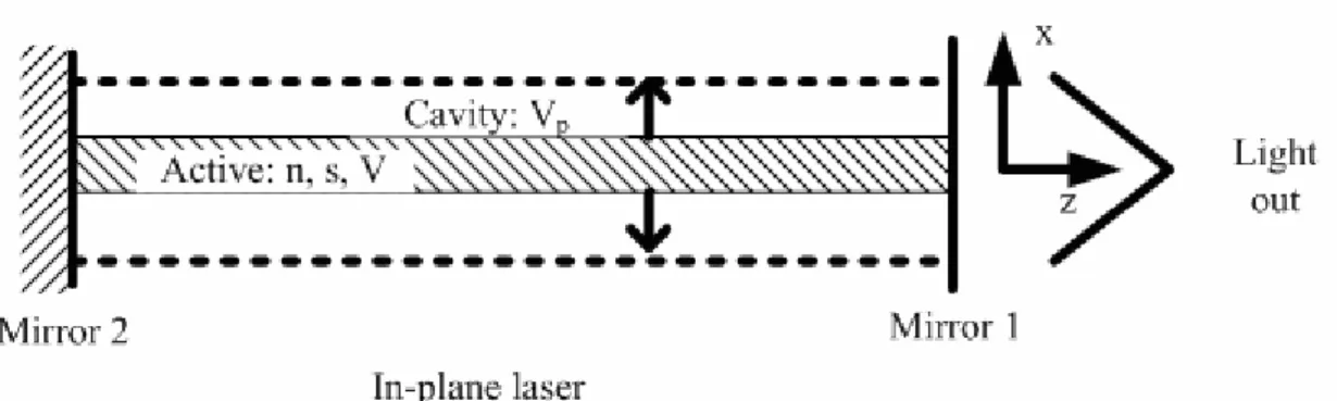
Fig. 2.5 Schematics of in-plane and vertical-cavity lasers illustrating the active (cross-hatched) and cavity (within dashed lines) volume as well as the coordinate systems.
[L. A. Coldren, and S. W. Corzine, Diode Lasers and Photonic Integrated Circuits, New York: Wiley Interscience, 1995.]
Fig. 2.6 Schematic of LED showing how only a small portion of the generated light reaches a desired detector.
[L. A. Coldren, and S. W. Corzine, Diode Lasers and Photonic Integrated Circuits, New York: Wiley Interscience, 1995.]
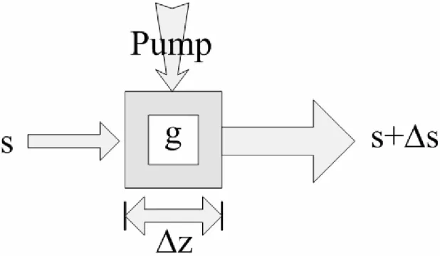
Fig. 2.7 Definition of gain in terms of the increase in photon number across a small segment of gain material.
Fig. 2.8 Maximum gain gmax and gain at a specific photon energy. [K. Petermann, Laser Diode Modulation and Noise, 1991]
Fig. 2.9 Generic laser cavity cross section showing active and passive sections and the guided-mode profile.
[L. A. Coldren, and S. W. Corzine, Diode Lasers and Photonic Integrated Circuits, New York: Wiley Interscience, 1995.]
Fig. 2.10 Reservoir analogy above threshold where water level has risen to the spillway so that an increased input results in an increased output (R ) but no increase in st carrier density (water level). The flows Rnr and Rsp do not change above
threshold.
[L. A. Coldren, and S. W. Corzine, Diode Lasers and Photonic Integrated Circuits, New York: Wiley Interscience, 1995.]
Fig. 2.11 Gain vs. carrier density and carrier density vs. input current. The carrier density clamps at threshold causing the gain to clamp also.
[L. A. Coldren, and S. W. Corzine, Diode Lasers and Photonic Integrated Circuits, New York: Wiley Interscience, 1995.]
Fig. 2.12 Illustration of output power vs. current for a diode laser. Below threshold only spontaneous emission is important; above threshold the stimulated emission power increases while the spontaneous emission is clamped at its threshold value.
[L. A. Coldren, and S. W. Corzine, Diode Lasers and Photonic Integrated Circuits, New York: Wiley Interscience, 1995.]
Fig. 2.13 Schematic illustration of modal gain versus injected carrier density with values labeled from the two-parameter logarithmic fit of Eq. (2.41).
[L. A. Coldren, and S. W. Corzine, Diode Lasers and Photonic Integrated Circuits, New York: Wiley Interscience, 1995.]
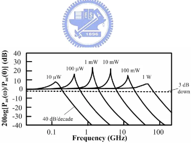
Fig. 2.14 Frequency response of an idealized diode laser for several different output powers.
[L. A. Coldren, and S. W. Corzine, Diode Lasers and Photonic Integrated Circuits, New York: Wiley Interscience, 1995.]
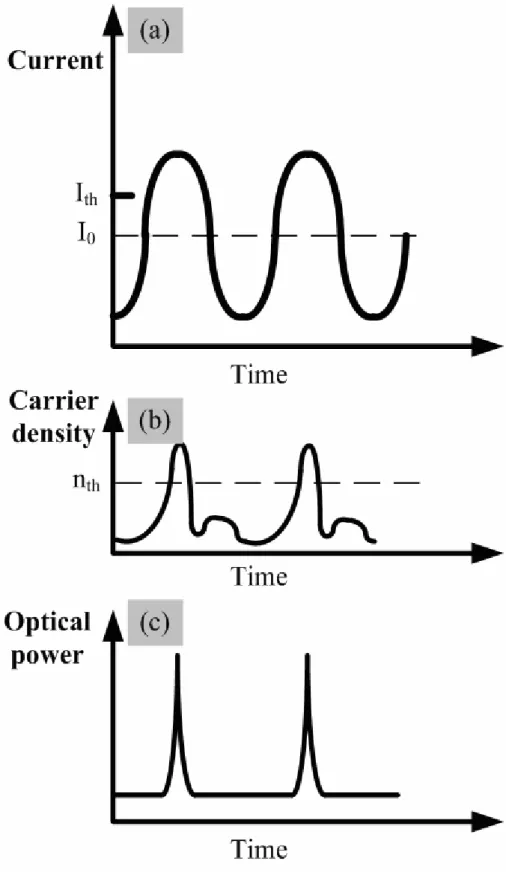
Fig. 3.1 The principle of gain switching. (a) The time dependence of the applied current; (b) The time dependence of the carrier density; (c) The time dependence of output pulses.
Fig. 3.2 (a) The ‘general’ gain-switching; (b) The injection-locking-induced gain-switching: (A) without external injection; (B) with external injection. Fig. 3.3 Experimental setup for the observation of the power-current curve with and
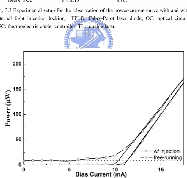
without external light injection locking. FPLD: Fabry-Perot laser diode; OC: optical circulator; TEC: thermoelectric cooler controller; TL: tunable laser. Fig. 3.4 Light-current (L-I) curves with and without external light injection locking. Fig. 3.5 Experimental setup for injection-locking-induced gain-switching. AMP: RF
amplifier; EDFA: erbium-doped fiber amplifier; FPLD: Fabry-Perot laser diode; TL: tunable laser; OBPF: optical bandpass filter; OC: optical circulator.
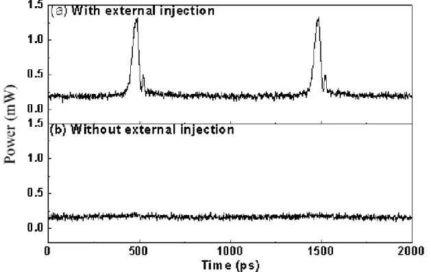
Fig. 3.6 The injection-locking-induced gain switching. (a) with external injection; (b) without external injection.
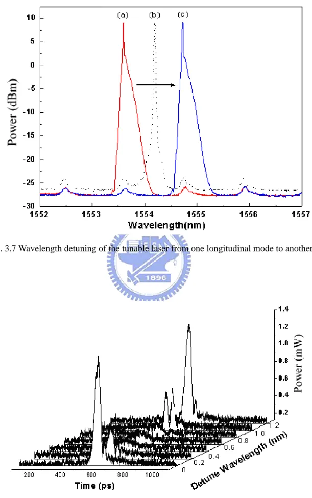
Fig. 3.7 Wavelength detuning of the tunable laser from one longitudinal mode to another.
Fig. 3.8 Temporal traces versus the detuning range.
Fig. 3.9 The injection-locking-induced pulse: (a) with injection locking at wavelengthλ ; (b) with injection locking at wavelengthλ+0.6nm; (c) without injection. The repetition rate of the pulse train is 1 GHz.
Fig. 3.10 Optical spectra of the FPLD modulated by a large sinusoidal signal at just below threshold: (a) injection locking; (b) injection with detuned
wavelength,λ+0.6nm; (c) without injection. It is noted that the red peak in trace (b) is the signal of the external injection light. The FPLD is not locked in this condition.
Fig. 3.11 Optical spectra: (a) modulated FPLD; (b) CW tunable laser; (c) CW FPLD injection-locked FPLD.
Fig. 3.12 The extinction ratio of the injection-locked FPLD at different RF driving and external injection power.
Fig. 3.13 The peak power and the SMSR of the single-mode gain-switched FPLD in injection-locking condition.
Fig. 3.14 The SSB phase noise density and the associated timing jitter of the injection-locking-induced pulses.
Fig. 3.15 Timing jitter and pulsewidth versus external injection power.
Fig. 3.16 Experimental setup for NRZ-to-RZ data format conversion. AMP: RF amplifier; EDFA: erbium-doped fiber amplifier; FPLD: Fabry-Perot laser diode; MZM: Mach-Zehnder intensity modulator; TL: tunable laser; OBPF: optical bandpass filter; OC: optical circulator; PG: pattern generator.
Fig. 3.17 The characteristic transmission coefficient of MZM at different DC bias. Fig. 3.18 RZ data streams (a) without OBPF (b) with OBPF.
Fig. 3.19 The patterns: (a) the electrical NRZ data before the MZM; (b) the PG-encoded optical NRZ data; (c) the transformed RZ signal generated from the single-mode FPLD. The data rate is 2.488 Gbit/s.
Fig. 3.20 The corresponding eye diagrams: (a) the electrical NRZ data before the MZM; (b) the PG-encoded optical NRZ data; (c) the transformed RZ data. The data rate is 2.488 Gbit/s.
Fig. 3.21 The BER performance at 2.488 Gbit/s. Fig. 3.22 The BER versus the external injection power.
Fig. 3.23 The dependence of operation data rate on FPLD’s DC bias current.
Fig. 3.24 The patterns: (a) the electrical NRZ data before the MZM; (b) the PG-encoded external injection light; (c) the converted RZ signal generated from the injection-locked FPLD. The data rate is 9.953 Gbit/s.
Fig. 3.25 The corresponding eye diagrams: (a) the electrical NRZ data before the MZM; (b) the PG-encoded external injection light; (c) the converted RZ signal generated from the single-mode FPLD. The data rate is 9.953 Gbit/s.
Fig. 3.26 The BER against the received optical power for NRZ-encoded external injection light and converted RZ signal at data rate of 9.953 Gbit/s.
Fig. 3.27 The BERs for different external injection powers at data rate of 9.953 Gbit/s. Fig. 4.1 Experimental setup and the truth table of the FPLD-based logic OR gate. AMP:
channel 2; EDFA: erbium-doped fiber amplifier; FPLD: Fabry-Perot laser diode; OBPF: optical bandpass filter; OC: optical coupler.
Fig. 4.2 The monitored data patterns. (a) and (b): two input NRZ data-streams; (c): passively combined data-stream; (d) the output data-stream (with the FPLD modulated at below threshold condition).
Fig. 4.3 The power dependent extinction ratio of the RZ-formatted data at rf-modulating power of (i) 24.4 dBm and (ii) 24.7 dBm. Inset: the conceptual diagrams of (i) the power-dependent and (ii) the power-independent OR gating operations. Fig. 4.4 P-I curves and of the rf-modulated and injection-locked FPLD for different
injection power.
Fig. 4.5 P-I slope of the rf-modulated and injection-locked FPLD for different injection power.
Fig. 4.6 The power-dependent (dotted trace) and power-independent (solid trace) logic OR output.
Fig. 5.1 Experimental setup for measurement of the dynamic chirp of the RZ-formatted data stream. DCM: dispersion compensation module.
Fig. 5.2 Experimental setup for 20-GHz soliton amplification and transmission. [M. Nakazawa, K. Suzuki, and Y. Kimura, Opt. Lett. 14, 1065 (1989).]
Fig. 5.3 Experimental setup for soliton transmission with a preemphasis technique using erbium-doped fiber amplifiers and repeaters.
[M. Nakazawa, K. Suzuki, and Y. Kimura, “3.2-5 Gb/s, 100 km Error-Free Soliton Transmissions with Erbium Amplifiers and Repeaters,” IEEE Photon. Technol. Lett. 2, 216 (1990).]
Fig. 5.4 Temporal trace of our RZ-formatted data by injection-locking the synchronously-modulated FPLD just below threshold current.
Fig. 5.5 Optical spectrum of the RZ-formatted data stream.
Fig. 5.6 Proposed experimental setup for soliton transmission for NRZ-to-RZ data format converter.
Fig. 5.7 Chirp characteristic in conventional gain-switching pulse. Fig. 5.8 Chirp characteristic of an injection-locking-induced pulse train. Fig. 5.9 Dynamic chirp of an injection-locking-induced data stream.
Fig. 5.10 Curves of the dispersion versus the wavelength for standard single mode fiber, Corning MetroCor fiber, and dispersion compensation fiber.
Fig. 5.11 Chirping results of RZ-formatted data stream after passing through different fibers.
List of Tables
Table 2.1 Typical parameter values for a 1.55 μm semiconductor laser in a injection-locking condition.
Table 3.1 Comparison among versatile NRZ-to-RZ techniques. Table 5.1 Formulas of calculation for excitingN = 1.4soliton.
Chapter 1
Introduction
1.1 Introduction of Semiconductor Lasers
To date semiconductor lasers have been considered the best light sources for high-bit-rate optical communication lines and fast optical data-processing systems. Compared to solid-state, gas, and dye lasers, the diode laser offers a considerably smaller size, higher efficiency, lower cost, and the unique ability to be modulated up to gigahertz rates by simply changing the driving current through the device. One of the main advantages of lightwave systems over electronic ones is their high speed and transmission capacity. The fundamental reason for this is the much higher carrier frequency of light (1014 to 1015 Hz) in a lightwave system. To realize the potentially very high capacity of lightwave system, the light source used should be able to generate short pulses at high repetition rates and capable of being modulated and encoded. These requirements are completely satisfied by using semiconductor laser diodes.
1.1.1 Historical Review of Semiconductor Lasers [1]
The advent of the laser dates back to 1958, the year in which the seminal paper of Schawlow and Townes appeared [2]. It was followed by the successful operation of a solid-state ruby laser [3] in May 1960 and of a He-Ne gas laser [4] in December 1960. The feasibility of stimulated emission in semiconductor lasers was considered during this period [5-7], and in 1962 several groups [8-11] reported the lasing action in semiconductors. The device consisted of a forward-biased GaAs p-n junction [8-10]. Electron-hole recombination in the depletion region of the p-n junction provided the optical gain, and the polished facets
perpendicular to the junction plane provided the optical feedback (by forming a resonant cavity)—the two necessary ingredients for any laser. Soon p-n junction of other direct-band-gap semiconductor materials such as InAs, InP, GaAsP, and InPAs were used to obtain semiconductor lasers at different wavelengths. Practical utility of these earlier devices was, however, limited since a large value of the threshold current density (Jth ≥50 kA/cm2) inhibited their continuous operation at room temperature.
As early as 1963 it was suggested [12, 13] that semiconductor lasers might be improved if a layer of one semiconductor material were sandwiched between two cladding layers of another semiconductor that has a relatively wider band gap. Such a device consisting of two dissimilar semiconductors is commonly referred to as a heterostructure laser, in contrast to the single-semiconductor devices, which are labeled as homostructure lasers. Both of these structures are shown schematically in Fig. 1.1, which also indicates their typical physical dimensions. Heterostructure lasers are further classified as single-heterostructure or double-heterostructure devices depending on whether the active region, where lasing occurs, is surrounded on one or both sides by a cladding layer of higher band gap. The use of a heterostructure, however, requires a careful matching of the lattice constants of the two semiconductors. It was only in 1969 that the successful room-temperature operation of a heterostructure laser was demonstrated [14-16] using the liquid-phase epitaxial technique [17] for the growth of GaAs and AlxGa1-xAs layers. However, these lasers operated in the pulsed mode. Further work led in 1970 to heterostructure lasers operating continuously at room temperature [18, 19]. Notation such as (Ga,Al)As or AlGaAs/GaAs is often used to emphasize the heterostructure nature of these GaAs lasers.
Already in 1969 double-heterostructure GaAs lasers with room-temperature value of 2
5 kA/cm th
J ≅ were reported [16]. This value was reduced [18] to about 1.6 kA/cm in 2
(~ 0.1 m thickμ ) active layers [20]. This was an improvement by more than two orders of magnitude over the simple homostructure lasers first made in 1962. It converted the semiconductor laser from a laboratory curiosity to a practical, compact, coherent light source useful for numerous applications.
The physical reason for the reduction in the threshold current density with the use of a heterostructure device is twofold [12, 13]. The cladding layers surrounding the active layer have a higher band gap and at the same time a lower refractive compared with those of the active layer (see Fig. 1.2). The band-gap difference helps to confine electrons and holes to the active layer, where they recombine to produce the optical gain. At the same time the refractive-index difference confines the optical mode close to the active layer, which acts as a dielectric waveguide. The optical-mode confinement significantly reduces the internal loss [14] that would otherwise occur in the absence of index guiding due to the spreading of the optical mode in the lossy regions.
A double-heterostructure semiconductor laser such as shown in Fig. 1.1 is sometimes called a broad-area laser since it does not incorporate any mechanism for the lateral (parallel to the junction plane) confinement of the injected current or the optical mode. As early as 1967, stripe-geometry homostructure lasers were proposed [21] to limit the lateral spread of the injected carriers inside the active layer, as shown in Fig. 1.3. In these lasers the current is injected over a narrow (~ 10 mμ ) central region using a stripe contact. The stripe geometry was adopted for heterostructure lasers [22] in 1971. Such lasers are also referred to as gain-guided (see Fig. 1.4a) since it is the lateral variation of the optical gain that confines the optical mode to the stripe vicinity [23]. By contrast, heterostructure lasers where the optical mode confinement occurs mainly through lateral variations of the refractive index are termed index-guided (see Fig. 1.4b). A large number of index-guided structures have been proposed and demonstrated over past decades. The literature is too vast to cite them individually, and a discussion of their relative merits can be found in several books [24-26] that also describe
the research and development effort for AlGaAs lasers up to 1980.
GaAs lasers are of continued interest. Using the growth techniques of vapor-phase epitaxy [27] and molecular-beam epitaxy [28], multiquantum-well laser structures have been developed [29]. In these devices the active region is not a single GaAs layer but rather consists of several thin (~ 0.01 mμ ) layers composed alternatively of GaAs and AlGaAs materials. Recently the emphasis has shifted toward high-power GaAs lasers and phased-array semiconductor lasers [30, 31]. In one approach, multiple stripes are used to generate distinct regions of optical gain in the junction plane and the near field consists of several spots. However, since the stripes are not widely separated, the optical field in the gain region of each emitter overlaps with that the neighboring emitter. Such a coupling leads to a phase-locked array of emitters providing well-collimated high power output. Whereas the output power from a conventional GaAs laser usually below 50 mW, more than 2 W of power has been obtained [31] by this technique of phase-locked arrays.
So far we have followed the development of GaAs lasers operating usually in the wavelength range of 0.8—0.9μm. Long-wavelength semiconductor lasers in the range of 1.1—1.6μm are of considerable interest for optical fiber communications [32]. Although several material systems were considered, the combination InGaAsP-InP turned out to be most suitable in view of its nearly perfect lattice match [33]. The active layer is composed of the In1-xGaxAsyP1-y quaternary alloy. By varying the mole fractions x and y, almost any wavelength in the 1.1—1.6μm range can be selected. The cladding layers in this heterostructure layer (see Fig. 1.1b) consist of either InP or InGaAsP itself with different mole fractions x and y.
Room-temperature operation of a 1.1-μm InGaAsP laser in the pulsed mode [34] was reported in 1975. The adoption of stripe geometry led to continuous operation [35] of such lasers in 1976. In 1977 the wavelength was extended [36] to 1.3 μm. Since low-loss
focused to develop a practical InGaAsP laser at this wavelength. Motivated by the realization [38] of an ultra-low-loss (~0.2 dB/km) fiber at the 1.55-μm wavelength, several groups [39-44] in 1979 reported on InGaAsP lasers operating in the vicinity of 1.55 μm. Since then the development effort for InGaAsP lasers operating in the wavelength range of 1.3—1.6μm has proceeded at an enormous pace [45-47]. The primary motivation is due to their application in optical fiber communications, and the use of InGaAsP lasers in long-haul optical communication systems has already reached the commercial stage [48].
1.1.2 Operating Principles of Semiconductor Lasers
This subsection is to provide a qualitative understanding of the physics behind the semiconductor laser. To form a laser, a gain medium and a feedback mechanism are both necessary. A gain medium, which is a semiconductor material in a semiconductor laser, can amplify the electromagnetic radiation propagating inside it and provide the spontaneous-emission noise input. A feedback mechanism, which is obtained using the cleaved facets of the semiconductor material that form a Fabry-Perot (FP) cavity, can confine the electromagnetic field through the well-defined optical modes. The mode confinement is achieved through dielectric waveguiding. A semiconductor laser needs to be externally pumped to obtain the optical gain, and both electrical and optical pumping techniques have been used for this purpose. A simple, practical, and most commonly used method employs current injection through the use of a forward-biased p-n junction. Such semiconductor lasers are sometimes referred to as injection lasers or laser diodes.
p-n Junction
A p-n junction [49] is formed by bringing a p-type and an n-type semiconductor into contact with each other. When they first come in contact, their quasi-Fermi levels do not match
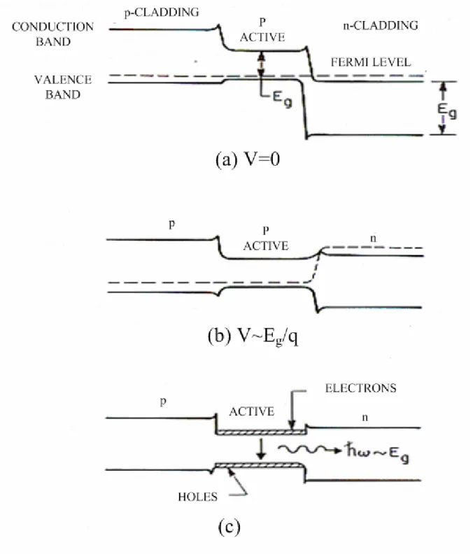
since the two are not in equilibrium. Equilibrium is, however, quickly established through diffusion of electrons from the n side to the p side, while the reverse occurs for holes. These diffusing electrons and holes recombine in the junction region. Eventually a steady state is reached in such a way that further diffusion of electrons and holes is opposed by the built-in electric field across the p-n junction arising from the negatively charged acceptors on the p side and the positively charged donors on the n side. The Fermi level is then continuous across the p-n junction, as shown in Fig. 1.5, where the energy-band diagram of the p-n homojunction (junction between two similar semiconductors) is shown.
When a p-n junction is forward-biased by applying an external voltage, the built-in electric field is reduced, making possible a further diffusion of electrons and holes across the junction. As Fig. 1.5b shows, in a narrow depletion region both electrons and holes are present simultaneously and can recombine either radiatively or nonradiatively. Photons of energy hν ≅Eg are emitted during radiative recombination. However, these photons can also be absorbed through a reverse process that generates electron-hole pairs. When the external voltage exceeds a critical value, a condition known as population inversion is achieved, in which the rate of photon emission exceeds that of absorption. The p-n junction is then able to amplify the electromagnetic radiation, whose wavelength satisfies
1.24 g E
λ≅ (1.1)
where Eg is the band gap of the semiconductor material in electron volts and the lasing wavelength λ is in micrometers. Therefore, the p-n junction is said to exhibit optical gain. However, for a homojunction the thickness of the region where gain is sufficiently high is very small (~ 0.01 mμ ) since there is no mechanism to confine the charge carriers, as shown in Fig. 1.1a.
double-heterostructure laser wherein the thin p-type active region has a lower band gap compared to that of the two p-type and n-type cladding layers. Electrons and holes can move freely to the active region under forward bias. However, once there, they cannot cross over to the other side because of the potential barrier resulting from the band-gap difference. This allows for a substantial build-up of the electron and hole population inside the active region, where they can recombine to produce optical gain. The width of the gain region is determined by the active-layer thickness, typically 0.1-0.3μm. As mentioned earlier, it was the adoption of the heterostructure scheme that resulted in significantly lower threshold current densities (compared with a homojunction) and led to the room-temperature operation of semiconductor lasers.
Dielectric Waveguide
The successful operation of a laser requires that the generated optical field should remain confined in the vicinity of the gain region. In double-heterostructure semiconductor lasers the optical confinement occurs by virtue of a fortunate coincidence. The active layer with a smaller band gap also has a higher refractive index compared with that of the surrounding cladding layers (see Fig. 1.2). Because of the index difference, the active layer in effect acts as a dielectric waveguide. The physical mechanism behind the confinement is total internal reflection, as illustrated in Fig. 1.7. When a ray traveling at an angle θ (measured from the interface normal) hits the interface, it is reflected back if the angle θ exceeds the critical angle θc given by
1 1
2
sin (critical angle) c μ θ μ − = (1.2)
where μ1 and μ2 are the refractive indices of the cladding and active layers, respectively. Thus, rays traveling nearly parallel to the interface are trapped and constitute the waveguide mode.
Recombination Mechanisms
When the current flowing through a semiconductor laser is increased, charge carriers (electrons and holes) are injected into the thin active region, where they recombine through radiative or nonradiative mechanisms. As one may expect, nonradiative recombinations are not helpful for laser operation, and attempts are made to minimize their occurrence by controlling point defects and dislocations. However, a nonradiative recombination mechanism, known as the Auger process, is intrinsic and becomes particularly important for long-wavelength semiconductor lasers operating at room temperature and above. Physically speaking, during the Auger process the energy released by the electron-hole recombination is taken by a third charge carrier and is eventually lost to lattice phonons. During a radiative recombination, the energy Eg released by the electron-hole pair appears in the form of a photon whose frequency ν or wavelength λ satisfies the energy
conservation relation Eg =hν =hc λ. This can happen through two optical processes known as spontaneous emission and stimulated emission. These are shown schematically in Fig. 1.8. In the case of spontaneous emission, photons are emitted in random directions with no phase relationship among them. Stimulated emission, by contrast, is initiated by an already existing photon. The remarkable feature is that the emitted photon matches the original photon not only in its wavelength but also in direction of propagation. I t is this relationship between the incident and emitted photons that renders the light emitted by a laser coherent.
Laser Threshold
Although stimulated emission can occur as soon as current is applied to the semiconductor laser, the laser does not emit coherent light until the current exceeds a critical value, known as the threshold current (Ith). This is so because stimulated
emission has to compete against the absorption processes during which an electron-hole pair is generated at the expense of an absorbed photon. Since the electron population in the valence band generally far exceeds that of the conduction band, absorption dominates. At a certain value of the external current, a sufficient number of electrons are present in the conduction band to make the semiconductor optically transparent. With a further increase in current, the active region of the semiconductor laser exhibits optical gain and can amplify the electromagnetic radiation passing through it. Spontaneously emitted photons serve as the noise input for the amplification process.
However, as mentioned above, a laser is formed by two necessary elements. The other necessary ingredient is optical feedback. In semiconductor lasers it is provided by the cleaved facets that form a Fabry-Perot (FP) cavity. The role of the FP cavity is twofold. First, it provides a directional selectivity for the process of stimulated emission, since only photons traveling along its axis are reflected back and forth. Second, it provides a wavelength selectivity since the feedback is strongest for wavelengths corresponding to the longitudinal modes of the FP cavity.
Because of the optical feedback, the number of photons traveling perpendicular to the facets increases when the current is large enough to satisfy the condition of net stimulated emission. However, some photons are lost through the partially transmitting facets and some get scattered or absorbed inside the cavity. If the loss exceeds the gain, stimulated emission cannot sustain a steady supply of photons. This is precisely what happens below threshold, when the laser output consists of mainly spontaneously emitted photons. At threshold, gain equals loss and stimulated emission begins to dominate. Over a narrow current range in the vicinity of the threshold current, the output power jumps by several orders of magnitude and the spectral width of the emitted radiation narrows considerably because of the coherent nature of stimulated emission.
Almost all electrons and holes injected into the active region now recombine through stimulated emission, and the internal quantum efficiency approaches 100%. The performance of a semiconductor laser is governed by a large number of emission characteristics related to the static, dynamic, and spectral behavior of the light output.
1.2 Enabling Technology for Data Format Conversion
Ultrafast all-optical signal processing techniques are expected to play a major role in future communications systems in order to avoid any optoelectronic speed bottlenecks. In future all-optical networks (AONs), relatively low bit rates (e.g. 1-2.5 Gbit/s) will be used preferably with non-return-to-zero (NRZ) format which requires minimal electronic bandwidth and has greater timing tolerance, as compared to the return-to-zero (RZ) format. However, the RZ data format is quite useful in applications including passive time-division-multiplexing (TDM) for increasing the network throughtput, soliton generation, and the suppression of stimulated Brillouin scattering [50, 51]. For these purposes, NRZ-to-RZ conversion is required. On the other hand, RZ-to-NRZ data format conversion is also necessary for reverse operation. There are versatile converters capable of transforming one format to the other [52-77]. In general, we divide these converters into two categories: RZ-to-NRZ and NRZ-to-RZ converters.In RZ-to-NRZ converters, it has been realized using many methods, including a nonlinear optical loop mirror (NOLM) [52], a semiconductor optical amplifier based wavelength converter [53], a cross-phase modulation in an SOA-based Mach-Zehnder interferometric wavelength converter [54, 55], a dual-wavelength injection locking in a Fabry-Perot laser diode (FPLD) [56], the spectral filtering from a cross-phase modulated signal in a dispersion-shifted fiber [57], and the spectral line-by-line control [58].
nonlinear active loop mirror (NALM) [59], a cross-gain compression-based wavelength converter [60], a nonlinear optical loop mirror (NOLM) [61, 62], a cross-phase modulation based single travelling wave semiconductor laser amplifier (TWSLA) [63], a gain-modulated semiconductor optical amplifier (SOA) [64], self-phase modulation (SPM) of SOA [65], a dual-wavelength injection locking in a FPLD [66], a cross-phase modulation in an SOA-based Mach-Zehnder interferometric wavelength converter [67], an optoelectronic oscillator (OEO) [68, 69], the transverse-magnetic mode absorption and SPM in a FPLD [70], an injection-locked FPLD at un-lasing condition [71-73], an SOA-loop-mirror [74], a Mach-Zehnder delay interferometer [75], and a dark-optical-comb injected SOA [76, 77].
In the following subsections, we will review two FPLD-based NRZ-to-RZ data format converters. In addition, techniques for generating short pulse (i.e. RZ format) in FPLDs are introduced. In the last subsection, we introduce injection locking in semiconductor lasers and the threshold current reduction induced by injection locking. These introductions are prepared for our novel FPLD-based NRZ-to-RZ data format converter, as shown in Section 1.3.
1.2.1 All-optical Non-Return-to-Zero (NRZ) to Return-to-Zero
(RZ) Data Format Conversion Technology by Using FPLDs
The Fabry-Perot laser diode (FPLD) based ultrafast all-optical signal processing techniques are expected to play important roles in future all-optical networks [66, 70, 78-81]. Versatile techniques such as the clock frequency division [79, 80], the wavelength conversion [81], and a nonreturn-to-zero (NRZ) to return-to-zero (RZ) format transformation [66, 70], have been demonstrated. Two featured works on the all-optical NRZ-to-RZ data format converters by using FPLDs are discussed. First, in 2002, Chow et al. [66] demonstrated an all-optical NRZ to RZ data format converter by using a cw-operated Fabry-Perot laser diode. They
used a dual-wavelength injection locking technique to achieve both wavelength and format conversion, as shown in Fig. 1.9. Later on, in 2004, Jeong et al. [70] used transverse-magnetic (TM) mode absorption of an FPLD and the self-phase modulation (SPM) technique to achieve NRZ-to-PRZ data format conversion for the aim to recover the data clock, as shown in Fig. 1.10.
1.2.2 Techniques for Generating Short Pulse
The first short pulse generation in diode lasers was the observation of irregular pulse trains emitted by a single-contact laser in 1966 [82]. Later on, the generation of regular picosecond pulses was first demonstrated in a double-section device in 1967 [83]. Since then, progress has continued both in experimental techniques and in theoretical understanding. In particular, significant progress has been made since 1978 when the first successful demonstration of the active mode locking of a laser with an external cavity was realized. In general, there are two reasons why one wants to pulse a laser light. One is that, although there may be less power on average in the beam, the instantaneous power in one of the laser flashes may be thousands of times greater than the power in a continuous wave light. The other is that a pulsed laser light can give information on very rapidly-occurring processes, rather like a photo-finish in a race. It’s a little like a very fast flash.
To obtain a pulsating light output, additional experimental manipulation must be performed with the laser. The simplest idea for generating laser pulses is to switch rapidly either gain or losses of the laser. Historically, the switching of diode-laser resonator quality or losses (Q-switching) was the first technique used to generate short light pulses [83]. Q-switching works in the following way. While the laser population inversion is building up, the switch is held in the “off” or high-loss state, ensuring a low Q. As the carrier density in the laser reaches its peak, the cavity is suddenly switched to the
high-Q condition, and the stored energy is rapidly emitted in an output optical pulse. The switching process can be initiated in one of two ways—active or passive. If the switching is caused by external influence, the technique is called as active Q-switching. However, there exists the possibility of passive/self-Q-switching of a laser by a bleachable (saturable) absorber. One feature of diode lasers is their ability to allow the ready incorporation of saturable absorbers of the same material as the active medium of the laser. As contrasted with other types of lasers, it is not necessary to have any external saturable absorber, but it is possible simply divide the diode into several sections and apply different currents to them. The parts of the laser with high current injection acts as the gain medium, while the unpumped sections or sections with a low pumping rate act as absorbers. Experimental Q-switched pulsewidths that have been obtained so far lie in the range of 2 to 30 ps at repetition rates above 10 GHz.
Another way for generating short pulses is gain switching [84-91]. Gain switching can be easily achieved in a diode laser by driving the laser with pulses or RF electrical currents. The first observations of relaxation oscillation when turning on a laser from below threshold have shown that short light pulses can be generated by direct modulation of the laser, with the optical puslewidth considerably shorter than the applied electrical pulses. The fundamental reason for this is an extremely short photon lifetime in a diode-laser cavity due to very small cavity length and relatively high cavity losses. The basic idea of gain switching consisted of the excitation of the first spike of relaxation oscillation and termination of the driving current before the onset of the following spikes. This can be achieved by applying either short electrical pulses or strong sine wave modulation on the laser. A typical pulsewidth of gain-switched pulses lies in the range of 10 to 30 ps at repetition rates up to several GHz.
Although gain switching and Q-switching are simple and attractive techniques for generating short pulses, the shortest laser pulses can be generated using another technique
known as mode locking. The term “mode locking” originates from the fact that, when the optical field is written in terms of the modes of the laser cavity, under mode-locked conditions all modes in the laser spectrum are in phase. In the case of the active mode locking of a diode laser, the pumping current is modulated at a frequency that corresponds accurately to the spacing of the cavity modes. The first attempt to initiate active mode locking by current modulation was made in 1971 but met only limited success that resulted in the generation of pulses of a few hundred picoseconds in duration [92]. Similar to self-Q-switching, passive mode locking can be achieved through the action of a saturable absorber without any external intervention (the first demonstration in 1968 [93]). A significant step forward in generating extremely short pulses in the femtosecond range was made with the introduction of colliding-pulse mode locking, which, in fact, is a modification of passive mode locking [94]. It was colliding-pulse mode locking of a diode laser with an external cavity that resulted in the significant reduction of pulsewidths of generated pulses in 1981. Another important step was made in 1989 when the monolithic (without external cavity) mode locking of a laser diode was demonstrated for the first time [95]. Using monolithic mode-locking diode lasers, it is possible to generate short optical pulses with very high repetition rates in excess of 100 GHz. Optical pulses of few hundred femtoseconds at repetition rates of 350 GHz can be obtained by mode-locked diode lasers [96].
1.2.3 Introduction of Injection Locking [97]
Injection locking of a semiconductor laser, with external coherent radiation injected into the laser cavity, appears to be drawing increasing attention [98-104]. Semiconductor diode lasers have a low Q factor cavity with the passband width as broad as several tens GHz and the gain spectrum several times broader, which is advantageous in achieving injection locking.
Recent progress in the diode laser fabrication technology has greatly improved the lasing characteristics, such as the mode stability and spectral purity, making injection locking a realistic subject for investigation. In one of the earlier reports it has been shown [99] that the waveform of the output response to a modulated exciting current can be greatly improved with light injection because the transient relaxation oscillation can be severely damped. Remarkable effects of the injection locking in controlling the spectrum and the frequency stability under direct modulation have recently been demonstrated [100, 101] and detailed experimental investigation on GaAs laser injection locking properties has been reported [102]. In 1994, Li [105] predicted that the gain is enhanced and hence threshold is decreased by including the spontaneous emission term. Later on, in 1998, Sivaprakasam and Singh [106] demonstrated the threshold current reduction experimentally by using two identical, single mode AlGaAs laser diodes (SDL 5412-H1,λ=850 nm).
1.3 Motivation of a novel FPLD-based NRZ-to-RZ
Converter
According to previous researches [60, 64], we know that the format conversion from NRZ to RZ can be obtained by manipulating the gain of device through an optical [60] (see Fig. 1.11) or an electrical [64] (see Fig. 1.12) method. Such a concept will be employed in an FPLD-based NRZ-to-RZ data format converter. First, it is well-known that the manipulation of the gain in FPLDs can be achieved by controlling the injection current. When the FPLD is gain-switched by using a sinusoidal wave or a short electrical pulse, it will generate an optical pulse, which is like the RZ signal. On the other hand, we experimentally observed that the threshold current of FPLDs can be reduced under external injection locking. Therefore, we combine these ideas and propose a new scheme to translate an NRZ-formatted optical data into an RZ-formatted optical data by biasing a synchronously-modulated FPLD at
un-lasing condition. In contrast to previous approaches, the FPLD used in our converter is operated just below threshold current by minimizing the DC driving current and appropriately setting the RF driving power. The FPLD becomes gain-switching when its threshold current is reduced by an external injection. That is, the FPLD receives the incoming NRZ data with high level (“1” bit), resulting in the generation of RZ data, whereas the low-level (“0” bit) data, ceasing the lasing of the FPLD. Such an external injection-locking not only achieves the NRZ-to-RZ conversion, but also helps to suppress the gain of side modes and the spontaneous emission, providing the FPLD output data stream a higher side mode suppression ratio (SMSR) and lower noise level.
1.4 Organization of Dissertation
The work described in this dissertation concentrates on the derivation of the reduction of the threshold current under external light injection locking condition and the application of this particular phenomenon in NRZ-to-RZ data format converter.
This dissertation is organized as follows: Chapter 2 derives the formula of the threshold current reduction. First, we will give a phenomenological approach, which is introduced by Coldren and Corzine, to diode lasers to derive the expression of the threshold current of diode lasers. Furthermore, by introducing the Li’s theory, we can derive the threshold current reduction under external light injection locking. Chapter 3 is the experimental setup and results of the FPLD-based NRZ-to-RZ converter. First, we use a continuous-wave (CW) light injection into the FPLD to observe the external light-injection-induced gain-switching. That is, the synchronously-modulated Fabry-Perot laser diode at below threshold condition becomes gain-switching when its threshold current is reduced by an external injection locking. Furthermore, we inject an incoming NRZ data stream into the FPLD, which receives the high level (“1” bit), resulting in the generation of a
RZ data, whereas receives the low-level (“0” bit), ceasing the lasing of the FPLD. Such an external injection-locking not only achieves the NRZ-to-RZ conversion, but also helps to suppress the gain of side modes and spontaneous emission, providing the FPLD output data-stream with a high side mode suppression ratio (SMSR) and low noise level. Chapter 4 is the experimental setup and results of an all-optical OR logic gate, which is realizes by using such an FPLD-based NRZ-to-RZ converter. In such an OR gate, the issue of pulse inequality is solved by slightly enlarging the amplitude of the RF modulating power. In Chapter 5, we propose a transmission configuration by using a preemphasis technique (proposed by Nakazawa et al.) to transmit the converted RZ data stream. The corresponding parameters for realizing this configuration are calculated. In addition, for evaluation of chirp of such a data format converter, a dynamic relative chirp measurement is constructed for observation of the results of chirp compensation and the chirp after transmission. Finally, Chapter 6 summarizes the dissertation and gives some future directions.
(a)
(b)
Fig. 1.1 Schematic illustration of (a) homostructure and (b) double-heterostructure semiconductor lasers with their typical physical dimensions. The dotted area represents the depletion region in the vicinity of the homojunction. The hatched area shows the thin (~0.2 μm) active layer of a semiconductor material whose band gap is slightly lower than that of the surrounding cladding layers.
[G. P. Agrawal, and N. K. Dutta, Long-wavelength Semiconductor Lasers, New York: Van Nostrand Reinhold, 1986.]
Fig. 1.2 Schematic illustration of the simultaneous confinement of the charge carriers and the optical mode to the active region occurring in a double-heterostructure semiconductor laser. The active layer has a lower band gap and a higher refractive index than those of the cladding layers.
[H. C. Casey, Jr., and M. B. Panish. Heterostructure Lasers, Parts A and B. New York: Academic Press, 1978.]
Fig. 1.3 Basic p+nn+ laser structure showing the stripe geometry contact which confines the active portion of the junction to a narrow region. The xyz axes are also defined.
[J. C. Dyment, “Hermite-gaussian Mode Patterns in GaAs Junction Lasers,” Appl. Phys. Lett.
Fig. 1.4 Two types of diode lasers with strong transverse confinement: (a) a gain-guided laser with poor lateral confinement; (b) an index-guided laser for strong lateral confinement. The current flow is laterally restricted by a strip of width w.
[Peter Vasil’ev, Ultrafast Diode Lasers: Fundamentals and Applications, Boston: Artech House Publishers, 1995]
Fig. 1.5 Energy-band diagram of a p-n junction at (a) zero bias and (b) forward bias. (c) Schematic representation of the electron and hole densities under forward bias. Radiative recombination of electrons and holes in the narrow overlapping region generates light.
[G. P. Agrawal, and N. K. Dutta, Long-wavelength Semiconductor Lasers, New York: Van Nostrand Reinhold, 1986.]
Fig. 1.6 Energy-band diagram of a double-heterostructure semiconductor laser at (a) zero bias and (b) forward bias. (c) The band-gap discontinuities at the two heterojunctions help to confine electrons and holes inside the active region, where they recombine to produce light. [G. P. Agrawal, and N. K. Dutta, Long-wavelength Semiconductor Lasers, New York: Van Nostrand Reinhold, 1986.]
Fig. 1.7 Dielectric waveguiding in a heterostructure semiconductor laser. The relatively higher refractive index ( μ2 >μ1) of the active layer allows total internal reflection to occur at the two interfaces for angles such that sinθ μ μ> 1 2.
[G. P. Agrawal, and N. K. Dutta, Long-wavelength Semiconductor Lasers, New York: Van Nostrand Reinhold, 1986.]
Fig. 1.8 Schematic illustration of (a) spontaneous-emission and (b) stimulated-emission processes wherein an electron-hole pair recombines to generate a photon. In the case of stimulated emission the two outgoing photons match in their frequency and direction of propagation.
[G. P. Agrawal, and N. K. Dutta, Long-wavelength Semiconductor Lasers, New York: Van Nostrand Reinhold, 1986.]
Fig. 1.9 Experimental setup. PC: polarization controller; SMF: single mode fiber; APD: avalanche photodiode; EDFA: erbium-doped fiber amplifier; BERT: bit-error tester.
[C. W. Chow, C. S. Wong, H. K. Tsang, “All-optical NRZ to RZ format and wavelength converter by dual-wavelength injection locking,” Opt. Commun. 209, 329 (2002).]
Fig. 1.10 Experimental setup for NRZ-to-PRZ converter; EDFA: erbium-doped fiber amplifier; PC: polarization controller; OBF: optical bandpass filter; PBS: polarization beam splitter.
[Y. D. Jeong, H. J. Lee, H. Yoo, and Y. H. Won, “All-optical NRZ-to-PRZ converter at 10 Gb/s based on self-phase modulation of Fabry-Perot laser diode,” IEEE Photon. Technol. Lett.
Fig. 1.11 Experimental setup. The gain-switched DFB3 is used to manipulate the gain in SOA1 and SOA2.
[J. P. R. Lacey, M. V. Chan, R. S. Tucker, A. J. Lowery and M. A. Summerfield, “All-optical WDM to TDM transmultiplexer,” Electron. Lett. 30, 1612 (1994).]
(a)
(b)
Fig. 1.12 (a) All-optical WDM-to-TDM node incorporating the modular functions of: (1) NRZ-to-RZ conversion; (2) extinction ratio enhancement; and (3) wavelength shifting. (b) Conceptual operation of the WDM-to-TDM node.
[D. Norte and A. E. Willner, “Demonstration of an all-optical data format transparent WDM-to-TDM network node with extinction ratio enhancement for reconfigurable WDM networks,” IEEE Photon. Technol. Lett. 8, 715 (1996).]
Chapter 2
Theory of Threshold Current Reduction
under External Light Injection Locking
2.1 Introduction
In this chapter we attempt to develop the theory about the threshold current reduction in semiconductor lasers under external light injection based on phenomenological arguments. By operating a Fabry-Perot laser diode in the condition of the external light injection locking, we can observe the phenomenon of the threshold current reduction through the L-I (light-current) curve measurement. Such a threshold current reduction is mainly attributed to injection locking in semiconductor lasers, which is a promising method to synchronize one or more free-running lasers to a master laser [107, 108]. Injection locking can be applied to ensure single mode operation [109], to generate optical frequency and phase modulation [110, 111], and to reduce the spectral width [112]. In addition, it can also be exploited to study the static and dynamic properties of the semiconductor lasers [113, 114].
From a fundamental point of view, the change of the lasing threshold current due to injection locking [115] is very important. It provides a tool to monitor the spontaneous emission into the laser mode and interplay between the charge carrier generation and recombination as both of them depend on the frequency, phase and intensity of the injected signal and the operating point of the laser.
Sharfin and Dagenais [116] predicted that optical injection does not lower the lasing threshold, since the optical light injection can only decrease the gain from the zero field value. In their work they had calculated the threshold current using the rate equation
approach. But they neglected the spontaneous emission part. The threshold current was taken when the average gain in the cavity becomes equal to the average loss rate. However, in 1994, Li [117] predicted that the gain is enhanced and hence threshold is decreased by including the spontaneous emission term. The behavior is quite complicated, especially for single mode diode lasers, where the linewidth enhancement factor and the cavity resonance dependence on the injected signal are more prominent.
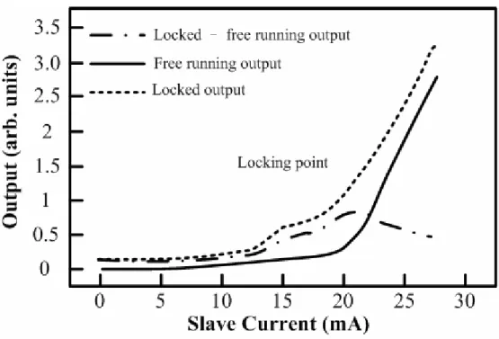
The reduction of the threshold current was demonstrated experimentally for the first time by Sivaprakasam and Singh [118]. They used two identical and single-moded AlGaAs laser diodes (SDL 5412-H1), whose emitting wavelength is around 850 nm. The one used for this study is termed the slave laser and the other providing the injected signal is termed the master laser. Both lasers are driven by ultra-low-noise current sources and temperature controlled by thermo-electric controllers to a precision of 0.01 K. As shown in Fig. 2.1, it is obvious that there is a reduction in the threshold current [118]. The threshold current taken is the point where there is sharp increase in the laser output. The injected power in this study is much less than the total increases hence there is a net increase in the gain. It is noted that the difference in power, which is proportional to the total gain change, was shown to have a maximum as the bias current approaches the threshold.
In Section 2.2, we introduce a phenomenological approach [119] to diode lasers. From a water reservoir model, we can derive a set of rate equations to describe the dynamics of carriers and photons. Furthermore, we adopt Li’s theory and consider the influence of the external light injection locking on the threshold current reduction in Section 2.3. These derivations are shown that the external light injection locking can reduce the threshold current of a semiconductor lasers.
2.2 A Phenomenological Approach to Diode Lasers [119]
In this section, a phenomenological approach, which is introduced by Coldren and Corzine [119], is used to derive the expression of the threshold current in diode lasers. First, a rate equation model is carried out for the flow of charge into double-heterostructure (DH) active regions and its subsequent recombination. Some electron-hole pairs recombine and generate photons by spontaneous emission, as shown in Fig 2.2a. This incoherent light by spontaneous emission is important in light-emitting diodes (LEDs). In subsequent subsection, we will derive the relevant equations governing LED operation for integrity of the theory. Furthermore, we provide a systematic derivation of the dc light-current characteristics of diode lasers. We begin from the development of the rate equation for photon generation and loss in a laser cavity. It shows that only a small portion of the spontaneously generated light contributes to the lasing mode. Most of the lasing light comes from the stimulated recombination of carriers. Such a stimulated carrier recombination/photon generation process, as shown in Fig. 2.2c, is a gain process. Next, the threshold gain, which is used to compensate for cavity losses, is studied. The current required to reach this gain is called the threshold current, and it is shown to be the current necessary to supply carriers for the unproductive nonradiative and spontaneous recombination processes, which clamp at their threshold value as more current is applied. Above threshold, all additional injected carriers are recombined in the active region to contribute to photons in the lasing mode by a stimulated recombination process. A fraction escape through the mirrors; others are absorbed by optical losses in the cavity.Finally, we introduce the modulation of lasers in Subsection 2.2.6. Under small-signal modulation, the rate equations for carriers and photons are found to be analogous to the differential equations that describe the current and voltage in an RLC circuit. Thus, the optical modulation response is found to have a resonance and to fall
off rapidly above this frequency. These derivations in Section 2.2 are prepared to obtain the injection-locking-induced reduction in the threshold current and the enhancement in the natural resonance frequency in FPLDs.
2.2.1 Carrier Generation and Recombination in Active Region
In a diode laser or LED, it is desirable to have all of the injected current contribute to electrons and holes which recombine in the active region. However, in practice only a fraction,ηi (i.e., internal quantum efficiency), of the injected current, I , does contribute such carriers. Figure 2.3 illustrates the process of carrier injection into a double-heterostructure active region.
The active region, where carriers are recombined to provide useful gain and photon emission, is usually the lowest bandgap region within the depletion region of a pin diode for efficient injection. However, it is occasionally convenient to include some of the surrounding intermediate bandgap regions. In the active region, there may be photon emission and even gain at some undesired wavelength elsewhere in the device. It is important to realize that the active region includes all of the injected carriers, not just carriers that recombine radiatively at the desired transition energy. The active regions analyzed here are undoped or lightly doped, so that under high injection levels relevant to LEDs and lasers, the electron density equals the hole density, i.e.,
n
=
p
in the active region due to charge neutrality. Therefore, for the simplicity, we proceed with our analysis by specifically tracking only the electron density,n
.The carrier density in the active region is governed by a dynamic process. Here, we use a water reservoir, which is being simultaneously filled and drained, to simulate the process of establishing a certain steady-state carrier density in the active region of the diode lasers, as shown schematically in Fig. 2.4. As we proceed, the various filling
(generation) and drain (recombination) terms illustrated will be defined. The current leakage illustrated in Fig. 2.4 contributes to current reduction
(
1−ηi)
I and is created by possible shunt paths around the active region. The carrier leakage,r
l, is due to carriers“splashing” out of the active region (by thermionic emission or by lateral diffusion if no lateral confinement exists) before recombining. Thus, this leakage contributes to a loss of carriers in the active region that could otherwise be used to generate light.
For the DH active region, a generation term is provided by the injected current into the active region,
η
iI , and recombination terms are provided by various radiative and nonradiative recombination processes as well as carrier leakage. Therefore, we have the rate equation asgen rec
dn
G R
dt = − (2.1)
whereGgenis the rate of injected electrons andRrecis the rate of recombining electrons per unit volume in the active region. Since there are
η
iI q
electrons per second being injected intothe active region, we can write the rate of injected electrons per unit volume as
i gen I G qV η = (2.2)
where
V
is the volume of the active region.The recombination process is a bit more complicated, since several mechanisms must be considered, including:
1. a spontaneous recombination rate,
r
sp(see Fig. 2.2a).2. a nonradiative recombination rate,
r
nr(see Fig. 2.2a).3. a carrier leakage rate,