Valence-band tunneling induced low frequency noise in ultrathin oxide ( 15 Å ) n -type
metal-oxide-semiconductor field effect transistors
J. W. Wu, J. W. You, H. C. Ma, C. C. Cheng, C. S. Chang, G. W. Huang, and T. Wang
Citation: Applied Physics Letters 85, 5076 (2004); doi: 10.1063/1.1827930 View online: http://dx.doi.org/10.1063/1.1827930
View Table of Contents: http://scitation.aip.org/content/aip/journal/apl/85/21?ver=pdfcov
Published by the AIP Publishing
Articles you may be interested in
A case study on the scaling of 1/f noise: La 2 / 3 Sr 1 / 3 MnO 3 Thin films
J. Appl. Phys. 113, 094901 (2013); 10.1063/1.4794202
Record of the lowest frequency shot noise measurement below 10 Hz
Appl. Phys. Lett. 91, 051916 (2007); 10.1063/1.2767234
Flicker ( 1 f ) noise in the critical current of Josephson junctions at 0.09 – 4.2 K
Appl. Phys. Lett. 85, 5296 (2004); 10.1063/1.1826236
Evidence for an additional noise source modifying conventional 1/f frequency dependence in sub-m metal–oxide–semiconductor field-effect transistors
Appl. Phys. Lett. 78, 380 (2001); 10.1063/1.1339252
A physical basis to Riemann hypothesis 1/f frequency noise
AIP Conf. Proc. 517, 538 (2000); 10.1063/1.1291289
This article is copyrighted as indicated in the article. Reuse of AIP content is subject to the terms at: http://scitation.aip.org/termsconditions. Downloaded to IP: 140.113.38.11 On: Thu, 01 May 2014 04:06:11
Valence-band tunneling induced low frequency noise in ultrathin oxide
„
15 Å
…
n
-type metal-oxide-semiconductor field effect transistors
J. W. Wu, J. W. You, H. C. Ma, and C. C. Cheng
Department of Electronics Engineering, National Chiao-Tung University, Hsinchu, Taiwan
C. S. Chang
Taiwan Semiconductor Manufacturing Company, Hsinchu, Taiwan
G. W. Huang
National Nano Device Laboratories, Hsinchu, Taiwan
T. Wanga)
Department of Electronics Engineering, National Chiao-Tung University, Hsinchu, Taiwan
(Received 22 July 2004; accepted 28 September 2004)
Low frequency flicker noise in n-type metal-oxide-semiconductor field effect transistors
(n-MOSFETs) with 15 Å gate oxide is investigated. A noise generation mechanism resulting from
valence band tunneling is proposed. In strong inversion condition, valence-band electron tunneling takes place and results in the splitting of electron and hole quasi-Fermi levels in the channel. The excess low frequency noise is attributed to electron and hole recombination at interface traps between the two quasi-Fermi levels. Random telegraph signal in a small area device is characterized to support our model. © 2004 American Institute of Physics. [DOI: 10.1063/1.1827930]
Drain current flicker noise in complementary metal-oxide-semiconductor(CMOS) transistors is an important de-sign parameter for high performance radio frequency(rf) and mixed mode circuits. It will affect the signal-to-noise ratio in operational amplifiers, analog-to-digital, and digital-to-analog converters. In addition, phase noise of voltage-controlled oscillators up-converted from flicker noise is an-other concern in rf applications.1
The origin of low frequency noise in n-MOSFETs with relatively thick gate oxides has been extensively studied. A unified noise model based on oxide charge tunnel trapping and detrapping has been adopted.2As gate oxide thickness is scaled into direct tunneling domain, oxide trap density is much reduced. In addition, channel electrons would likely tunnel through an ultrathin gate oxide directly without being captured by oxide traps. However, the low frequency noise in ultrathin oxide CMOS devices still exhibits a noticeable level.3In this work, the low frequency noise in n-MOSFETs with a 15 Å gate oxide is investigated. The electron trapping/ detrapping times are characterized from random telegraph signal (RTS) in small area n-MOSFETs. The normalized noise power spectral density共Sid/ Id
2兲 is also measured as a
monitor of drain current noise, which is considered as a fair index because of the normalization to the drain current. Fi-nally, a new generation/recombination noise mechanism as a result of valence band electron tunneling will be proposed to explain the observed noise behavior.
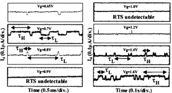
Figure 1 shows typical RTS patterns in a small area
共W/L=0.16m / 0.12m兲15 Å gate oxide n-MOSFET at various gate voltages 共Vg兲 from weak inversion to strong inversion. The drain bias in RTS measurement is 0.1 V to assure a uniform charge distribution in the channel. Due to a single charge trapping/detrapping, the RTS exhibits two lev-els. HandL in the figure denote the time in high current state (empty trap) and in low current state (occupied trap),
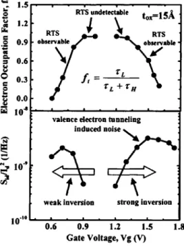
respectively. The electron occupation factor of the trap 共ft兲 can be evaluated as ft=L/共L+H兲. Figure 2 shows ft and corresponding Sid/ Id
2 (measured at V
d= 0.1 V, f = 100 Hz) vs
Vg from weak inversion to strong inversion. In weak inver-sion region(i.e., Vg⬍0.9 V),LandHcorresponds to elec-tron emission and capture time through an interface trap
(shown in Fig. 3). As Vgincreases,Hdecreases,Lincreases and thus ft increases because of increased channel electron population. As ft increases to 1, RTS becomes undetectable
(Fig. 1) since the trap is always occupied by an electron.
Thus, Sid/ Id
2 has a peak around f
t⬃0.5 in Fig. 2. The ob-served Vg dependence of L and H in weak inversion is consistent with the findings for thicker gate oxides in other publication.4 However, we find that the RTS patterns in strong inversion共Vg⬎1 V兲 exhibit an opposite trend. The Vg
dependence of Hand L in strong inversion is opposite to that in weak inversion. Moreover, significant substrate
cur-rent is noticed for Vg⬎1 V (not shown here) because valence-band electron tunneling occurs and generated holes flow to the substrate.
a)Electronic mail: [email protected]
FIG. 1. Typical characteristics of two-level RTS(measured at Vd= 0.1 V) at
various gate voltages in a small area n-MOSFET (W/L=0.16m / 0.12
m, tox= 15 Å). RTS is undetectable at Vg= 0.9 V, and 1 V.
APPLIED PHYSICS LETTERS VOLUME 85, NUMBER 21 22 NOVEMBER 2004
0003-6951/2004/85(21)/5076/2/$22.00 5076 © 2004 American Institute of Physics
This article is copyrighted as indicated in the article. Reuse of AIP content is subject to the terms at: http://scitation.aip.org/termsconditions. Downloaded to IP: 140.113.38.11 On: Thu, 01 May 2014 04:06:11
In strong inversion regime, ft declines with Vg from unity and the noise level shows another peak(Figs. 1 and 2). This means, at a larger Vg, although the energy level of the interface trap is deeper with respect to the electron Fermi level, the chance of the trap being occupied by an electron becomes smaller. The result is quite different from the equi-librium case that ft should increase as the trap energy
be-comes more negative with respect to the Fermi level. The possible explanation is illustrated in Fig. 3. A larger Vg causes strong valence electron tunneling and leaves more holes behind in the channel. The nonequilibrium carrier dis-tribution results in the splitting of electron and hole quasi-Fermi-levels. Because of the increased channel hole concen-tration at a larger Vg, the hole capture time 共L兲 is smaller, leading to a reduced ft. The second peak of Sid/ Id
2
in strong inversion condition 共Vg⬎1 V兲 in Fig. 2 thus can be well understood.
For a comparison, the ftand Sid/ Id
2
vs Vgin a thicker gate oxide共33 Å兲 n-MOSFET are also characterized (Fig. 4). In contrast, the ftstays at unity in strong inversion. Neither RTS nor the second noise peak is detected since valence-bane tunneling is negligible in such thick gate oxide devices.
In summary, an abnormal noise behavior in ultrathin ox-ide n-MOSFETs is observed in strong inversion condition. The traditional flicker noise model cannot account for the observed low-frequency noise. The analysis of RTS patterns reveals that the increased channel hole concentration and a Fermi-level splitting due to valence-band electron tunneling is responsible for the excess low-frequency noise.
The authors would like to thank TSMC, Taiwan for pro-viding technical and financial support. Financial support from National Science Council, Taiwan under Contract No. NSC92-2215-E009-024 is greatly appreciated.
1
A. Hajimiri and T. H. Lee, IEEE J. Solid-State Circuits 33, 179(1998).
2
K. K. Hung, P. K. Ko, C. Hu, and Y. C. Cheng, IEEE Trans. Electron Devices 37, 654(1990).
3
M. J. Knitel, P. H. Woerlee, A. J. Scholten, and A. T. A. Zegers-Van Duijnhoven, Tech. Dig. - Int. Electron Devices Meet. 2000, 463(2000). 4
K. Kandiah, M. O. Deighton, and F. B. Whiting, J. Appl. Phys. 66, 937
(1989).
FIG. 2. Electron occupation factor共ft兲 and normalized noise power spectral
density(measured at Vd= 0.1 V and f = 100 Hz) vs gate voltage in a small
area n-MOSFET(W/L=0.16m / 0.12m, tox= 15 Å). The second noise
peak in strong inversion is due to valence-band electron tunneling.
FIG. 3. RTS in weak inversion condition results from electron capture共H兲
and electron emission共L兲 at an interface trap; RTS in strong inversion
condition results from electron capture 共H兲 and hole capture 共L兲 at an
interface trap.
FIG. 4. Electron occupation factor共ft兲 and normalized noise power spectral
density(measured at Vd= 0.1 V and f = 100 Hz) vs gate voltage in a small
area n-MOSFET(W/L=0.24m / 0.18m) with tox= 33 Å.
Appl. Phys. Lett., Vol. 85, No. 21, 22 November 2004 Wuet al. 5077
This article is copyrighted as indicated in the article. Reuse of AIP content is subject to the terms at: http://scitation.aip.org/termsconditions. Downloaded to IP: 140.113.38.11 On: Thu, 01 May 2014 04:06:11