Very High Density
„44 fF/m
2… SrTiO
3MIM Capacitors for
RF Applications
K. C. Chiang,a,zJ. W. Lin,bH. C. Pan,cC. N. Hsiao,cW. J. Chen,dH. L. Kao,e I. J. Hsieh,band Albert China,
*
a
Department of Electrical Engineering, Nano-Science Technology Center, National Chiao-Tung University, University System of Taiwan, Hsinchu, Taiwan
b
Department of Electric Engineering, Chung Hua University, Hsinchu, Taiwan
c
Instrument Technology Research Center, National Applied Research Laboratories, Hsinchu, Taiwan
d
Graduate Institute of Materials Engineering, National Ping-Tung University of Science and Technology, Taiwan
e
Department of Electronic Engineering, Chang-Gung University, Hsinchu, Taiwan
We demonstrate a high-performance TaN/SrTiO3/TaN metal-insulator-metal 共MIM兲 radio-frequency 共rf兲 capacitor with good device integrity of very high capacitance density of 44 fF/m2, small voltage linearity␣ of 54 ppm/V2at 2 GHz, and a small capacitance reduction 3.5% from 100 KHz to 10 GHz. Such large capacitance density can largely reduce the device size used in rf integrated circuits.
© 2007 The Electrochemical Society. 关DOI: 10.1149/1.2431323兴 All rights reserved.
Manuscript submitted May 10, 2006; revised manuscript received November 13, 2006. Available electronically January 19, 2007.
Based on the International Technology Roadmap for
Semicon-ductors (ITRS), continuous down-scaling of the device size of
radio-frequency共rf兲 capacitors is needed to reduce the die size and lower the costs. To meet this requirement, higher capacitance density 共0/td兲 is required and using higher dielectric constant 共兲 material is the only choice.1-16This is because the decreasing dielectric thick-ness共td兲 results in the degraded device performance of higher leak-age current and poorer voltleak-age-dependence of capacitance共⌬C/C兲. Because the high strontium titanate 共SrTiO3兲17-19dielectric has a very high value 共reachable to 300兲 beyond HfO2共 ⬃ 22 − 24兲, Nb2O5共 ⬃ 40兲,11TaTiO共 ⬃ 45兲,15,16or HfTiO, it is important to study the possibility for rf applications. In addition, the SrTiO3 共STO兲 is also listed in the DRAM manufacture roadmap,20
and therefore the STO capacitor may be used for analog, rf, and dynamic random access memory共DRAM兲 simultaneously to realize low pro-cess costs and multifunctional system-on-chip共SoC兲. In this paper, we have studied STO metal-insulator-metal共MIM兲 capacitor for rf applications. Very high capacitance density of 44 fF/m2, high value of 147, and small⌬C/C of 752 ppm at 2 GHz were obtained at the same time, demonstrating the excellent device performance for rf applications.
Experimental
After depositing 2m of SiO2on Si wafer, the lower capacitor electrode was formed using plasma vapor deposited共PVD兲 TaN/Ta bi-layers. After patterning the bottom electrode, the TaN was treated by NH3plasma nitridation. Largely improved interfacial TaON for-mation, oxygen deficiency, and capacitance density degradation were achieved after post-deposition anneal共PDA兲.21Then, the 26 and 30 nm thick STO layers were deposited on the TaN/Ta elec-trode by PVD, followed by 450°C PDA for 1 h under oxygen envi-ronment. Finally, the TaN/Al was deposited and patterned to form the top capacitor electrode. The fabricated rf MIM capacitors were characterized using an HP4284A precision LCR meter to 1 MHz, and an HP8510C network analyzer for the S-parameter measure-ments to 10 GHz.8,9The series parasitic impedance and parallel rf pads were de-embedded from ‘through’ and ‘open’ transmission lines,15,22 respectively. The capacitance at rf frequency was ex-tracted from the measured S-parameters using an equivalent circuit model.8,9,15,16
Results and Discussion
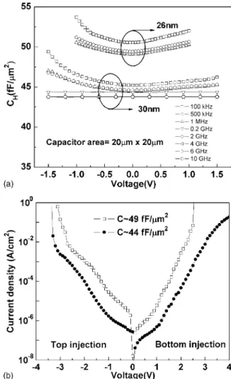
Figures 1a and b show the capacitance-voltage 共C-V兲 and current-voltage 共J-V兲 characteristics of STO MIM capacitors,
re-*Electrochemical Society Active Member.
z
E-mail: [email protected]
Figure 1.共a兲 C-V and 共b兲 J-V characteristics of STO MIM capacitors. The C-V results from 100 kHz to 1 MHz are measured from LCR meter and the data from 0.2 GHz to 10 GHz was obtained from the S-parameters. High capacitance density of 44 and 49 fF/m2were measured with low leakage density of 5⫻ 10−7and 6⫻ 10−6A/cm2.
Journal of The Electrochemical Society, 154共3兲 H214-H216 共2007兲 0013-4651/2007/154共3兲/H214/3/$20.00 © The Electrochemical Society
H214
) unless CC License in place (see abstract).
ecsdl.org/site/terms_use
address. Redistribution subject to ECS terms of use (see
140.113.38.11
spectively. Very high capacitance density of 44 and 49 fF/m2 or capacitance-equivalent thickness共CET兲 of 0.78 and 0.70 nm were measured with low leakage of 5⫻ 10−7and 6⫻ 10−6A/cm2, re-spectively. Such small CET is useful for ITRS 45 nm node DRAM at year 2010. The leakage current under positive bias共electron in-jected from bottom TaN兲 is slightly lower than that under reverse bias共electron injected from top TaN兲. This may be due to the rough top STO surface from STO crystallization, which creates localized higher electric field in top TaN/STO. The surface roughness be-tween dielectric and electrode is usually responsible for asymmetric performance of MIM capacitors.23In addition, note that the leakage current of 5⫻ 10−7A/cm2 is low enough for rf integrated circuit 共IC兲 applications due to the very high capacitance density of 44 fF/m2: for a typically large 1 pF capacitor used in rf IC, the leakage current is as low as 0.1 pA at 1 V and significantly lower than the leakage current of sub-100 nm transistors.22Furthermore, a near constant capacitance value with little voltage and frequency dependence is obtained for the STO MIM capacitor, which is im-portant for rf IC under large voltage swing condition.
To study the current conduction mechanism of TaN/STO/TaN MIM capacitors, we have plotted ln共J兲 vs E1/2in Fig. 2. Here, both Schottky emission共SE兲 and Frenkel-Poole 共FP兲 conduction can give a linear ln共J兲-E1/2relation with different slopes共␥兲, as shown by
J⬀ exp
冉
␥E 1/2− V b kT冊
关1兴 ␥ =冉
e3 0K⬁冊
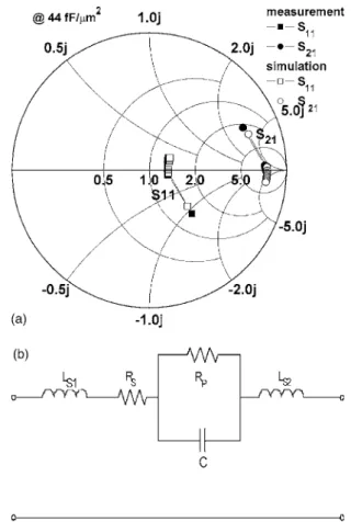
1/2 关2兴 where K⬁ is the high-frequency dielectric constant 共=n2; n is the refractive index and equals to 2.4 for STO18,19兲, and is a constant with value of 1 or 4 for FP or SE, respectively. From the good matching between measured and Eq. 1 calculated data, the current conduction mechanism changes from SE at low electric fields to FP at higher fields.To investigate the device rf characteristics of STO MIM capaci-tors, the S-parameters were measured. Figure 3a shows the mea-sured S-parameters for TaN/STO/TaN capacitors, and the capaci-tance value is extracted by using the equivalent circuit model shown in Fig. 3b. The MIM capacitor is modeled by Rpand C, where the Rporiginates from the high- dielectric loss. In addition, the Rs, Ls1, and Ls2represent the parasitic impedances in the coplanar transmis-sion line used for rf measurements. Good matching between mea-sured and modeled S-parameters are shown in Fig. 3a, indicating the good accuracy for capacitance extraction at rf regime beyond the limited 1 MHz of LCR meter.
The obtained capacitance density is plotted in Fig. 4a. Small capacitance reduction of only 3.5% to 10 GHz is indicative of the
good device performance over the whole intermediate frequency 共IF兲 to rf range.6,7 However, such extracted capacitance density at the rf regime is not sensitive enough to calculate the small⌬C/C variation, important for precision capacitors operated under large signal swing. We have used the previous circuit-theory-derived equation8to calculate the⌬C/C-V from measured S-parameters and the results are shown in Fig. 4b. The measured⌬C/C-V can be fitted with a second order polynomial equation, where linear共兲 and qua-dratic共␣兲 voltage coefficients of ⌬C/C were obtained. Because the  effect can be canceled by circuit design using differential method, ␣ is the key parameter to cause the unwanted voltage-dependent ⌬C/C. The obtained ⌬C/C and ␣ are also plotted in Fig. 4a. Fortu-nately, both␣ and ⌬C/C decrease with increasing frequency into the rf region, which is attributed to the trapped carriers being unable to follow the high-frequency signal with typical carrier lifetimes in the range ms to s.8,9,15,16 Therefore, high capacitance density of 44 fF/m2, small⌬C/C of 752 ppm, and low ␣ of 54 ppm/V2at 2 GHz are important for high-speed rf IC applications.
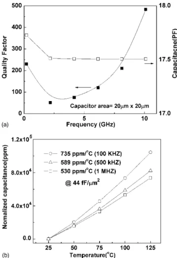
The device quality共Q兲 factor and corresponding capacitance ex-tracted from the circuit model6using the S-parameters at rf frequen-cies is shown in Fig. 5a. Note that a good Q-factor⬎50 is obtained for rf application before resonant frequency共 fr兲 of ⬃13 GHz, where the relative low fr is due to the large capacitance. Furthermore, because the advanced ICs are usually operated at higher temperature due to power dissipation, the temperature-coefficient on capacitance 共TCC兲 is another important factor. Figure 5b shows the TCC ob-tained from normalized capacitance of STO capacitor as a function of temperatures. Again, the TCC decreases with increasing fre-quency with TCC values close to previous TiTaO devices.15
Figure 2. Measured and simulated J-E1/2of STO MIM capacitors.
Figure 3.共a兲 Measured and simulated two-port S-parameters for STO MIM capacitors, from 500 MHZ to 10 GHz and共b兲 equivalent circuit model for capacitor simulation in rf regime.
H215
Journal of The Electrochemical Society, 154共3兲 H214-H216 共2007兲 H215
) unless CC License in place (see abstract).
ecsdl.org/site/terms_use
address. Redistribution subject to ECS terms of use (see
140.113.38.11
Conclusions
Very high 44 fF/m2capacitance density, small capacitance re-duction of 3.5% to 10 GHz, and a small␣ of 54 ppm/V2at 2 GHz were simultaneously achieved in TaN/STO/TaN capacitors pro-cessed at 450°C and important for rf application. This high-density MIM capacitor is important for down-scaling the capacitance size and integration with DRAM.
Acknowledgment
This work has been partially supported by NSC 共95-2221-E-009-298兲 of Taiwan.
National Chiao Tung University assisted in meeting the publication costs of this article.
References
1. C. H. Ng, K. W. Chew, and S. F. Chu, IEEE Electron Device Lett., 24, 506共2003兲. 2. L. Y. Tu, H. L. Lin, L. L. Chao, D. Wu, C. S. Tsai, C. Wang, C. F. Huang, C. H. Lin, and J. Sun, in Proceedings of the Symposium on VLSI Technology, IEEE, p. 79 共2003兲.
3. Z. Chen, L. Guo, M. Yu, and Y. Zhang, IEEE Microw. Wirel. Compon. Lett., 12, 246共2002兲.
4. J. A. Babcock, S. G. Balster, A. Pinto, C. Dirnecker, P. Steinmann, R. Jumpertz, and B. El-Kareh, IEEE Electron Device Lett., 22, 230共2001兲.
5. C.-M. Hung, Y.-C. Ho, I.-C. Wu, and K. O, IEEE Trans. Microwave Theory Tech., 46, 505共1998兲.
6. S. B. Chen, J. H. Lai, K. T. Chan, A. Chin, J. C. Hsieh, and J. Liu, IEEE Electron Device Lett., 23, 203共2002兲.
7. S. B. Chen, J. H. Lai, A. Chin, J. C. Hsieh, and J. Liu, IEEE Electron Device Lett.,
23, 185共2002兲.
8. C. H. Huang, M. Y. Yang, A. Chin, C. X. Zhu, M. F. Li, and D. L. Kwong, in Proceedings of the IEEE MTT-S International Microwave Symposium, IEEE, p. 507 共2003兲.
9. M. Y. Yang, C. H. Huang, A. Chin, C. Zhu, B. J. Cho, M. F. Li, and D. L. Kwong, IEEE Microw. Wirel. Compon. Lett., 13, 431共2003兲.
10. C. Zhu, H. Hu, X. Yu, A. Chin, M. F. Li, and D. L. Kwong, Tech. Dig. - Int. Electron Devices Meet., 2003, 379.
11. S. J. Kim, B. J. Cho, M.-F. Li, C. Zhu, A. Chin, and D. L. Kwong, in Proceedings of the Symposium on VLSI Technology, IEEE, p. 77共2003兲.
12. S. J. Kim, B. J. Cho, M.-F. Li, S.-J. Ding, C. Zhu, M. B. Yu, B. Narayanan, A. Chin, and D.-L. Kwong, IEEE Electron Device Lett., 25, 538共2004兲.
13. S. J. Kim, B. J. Cho, M. B. Yu, M.-F. Li, Y.-Z. Xiong, C. Zhu, A. Chin, and D. L. Kwong, in Proceedings of the Symposium on VLSI Technology, IEEE, p. 56共2005兲. 14. S. J. Kim, B. J. Cho, M. B. Yu, M. F. Li, Y. Z. Xiong, C. Zhu, A. Chin, and D. L.
Kwong, IEEE Electron Device Lett., 26, 625共2005兲.
15. K. C. Chiang, C. H. Lai, A. Chin, T. J. Wang, H. F. Chiu, J. R. Chen, S. P. McAlister, and C. C. Chi, IEEE Electron Device Lett., 26, 728共2005兲. 16. K. C. Chiang, A. Chin, C. H. Lai, W. J. Chen, C. F. Cheng, B. F. Hung, and C. C.
Liao, in Proceedings of the Symposium on VLSI Technology, IEEE, p. 62共2005兲. 17. P.-Y. Lesaicherre, S. Yamamichi, H. Yamaguchi, K. Takemura, H. Watanabe, K. Tokashiki, K. Satoh, T. Sakuma, M. Yoshida, S. Ohnishi, K. Nakajima, K. Shiba-hara, Y. Miyasaka, and H. Ono, Tech. Dig. - Int. Electron Devices Meet., 1994, 831.
18. C.-J. Peng, H. Hu, and S. B. Krupanidhi, Appl. Phys. Lett., 63, 1038共1993兲. 19. F. Gervais, in Handbook of Optical Constants of Solids, E. D. Palik, Editor, p.
1035, Academic Press, New York共1991兲.
20. K. Kim, Tech. Dig. - Int. Electron Devices Meet., 2005, 333.
21. K. C. Chiang, C. C. Huang, A. Chin, G. L. Chen, W. J. Chen, Y. H. Wu, and S. P. McAlister, IEEE Trans. Electron Devices, 53, 2312共2006兲.
22. M. C. King, Z. M. Lai, C. H. Huang, C. F. Lee, D. S. Yu, C. M. Huang, Y. Chang, and Albert Chin, in Proceedings of the IEEE RF-IC Symposium, IEEE, p. 171 共2004兲.
23. N. Gaillard, L. Pinzelli, and G.-J. Mickael, Appl. Phys. Lett., 89, 133506共2006兲. Figure 4.共a兲 Frequency dependent capacitance density, ⌬C/C, and ␣ for a
STO MIM capacitor biased at 1.5 V. The data for frequencies⬎1 MHz was obtained from the S-parameters.共b兲 The ⌬C/C-V characteristics of a STO MIM capacitor at rf regime.
Figure 5.共a兲 Q-factor of TaN/STO/TaN MIM capacitors biased at 1.5 V 共b兲 The temperature-dependent normalized capacitance共TCC兲 with different fre-quency. The capacitor size is 20⫻ 20 m.
H216 Journal of The Electrochemical Society, 154共3兲 H214-H216 共2007兲
H216
) unless CC License in place (see abstract).
ecsdl.org/site/terms_use
address. Redistribution subject to ECS terms of use (see
140.113.38.11