Wide angle distributed Bragg reflectors for 590 nm amber AlGaInP light-emitting diodes
S. W. Chiou, C. P. Lee, C. K. Huang, and C. W. ChenCitation: Journal of Applied Physics 87, 2052 (2000); doi: 10.1063/1.372135 View online: http://dx.doi.org/10.1063/1.372135
View Table of Contents: http://scitation.aip.org/content/aip/journal/jap/87/4?ver=pdfcov
Published by the AIP Publishing
Articles you may be interested in
Metal mirror assisting light extraction from patterned AlGaInP light-emitting diodes
Appl. Phys. Lett. 94, 101102 (2009); 10.1063/1.3097017
Forward current-voltage characteristics of an AlGaInP light-emitting diode
J. Appl. Phys. 102, 043706 (2007); 10.1063/1.2772530
Effect of current spreading on luminescence improvement in selectively oxidized AlGaInP light-emitting diodes
J. Vac. Sci. Technol. B 21, 1157 (2003); 10.1116/1.1577572
Improved characteristics of InGaN multiple-quantum-well light-emitting diode by GaN/AlGaN distributed Bragg reflector grown on sapphire
Appl. Phys. Lett. 76, 1804 (2000); 10.1063/1.126171
AlGaInP light-emitting diodes with mirror substrates fabricated by wafer bonding
Appl. Phys. Lett. 75, 3054 (1999); 10.1063/1.125228
[This article is copyrighted as indicated in the article. Reuse of AIP content is subject to the terms at: http://scitation.aip.org/termsconditions. Downloaded to ] IP: 140.113.38.11 On: Thu, 01 May 2014 07:57:51
Wide angle distributed Bragg reflectors for 590 nm amber AlGaInP
light-emitting diodes
S. W. Chiou and C. P. Lee
Department of Electronics Engineering, National Chiao Tung University, Hsinchu, Taiwan, Republic of China
C. K. Huang and C. W. Chen
Opto-Electronics and Systems Laboratories, Industrial Technology Research Institute, Hsinchu, Taiwan, Republic of China
共Received 1 July 1999; accepted for publication 2 November 1999兲
A structure for high brightness light-emitting diodes共LEDs兲 is demonstrated. A distributed Bragg reflector共DBR兲 is used to enhance the quantum efficiency of the LEDs. This unique DBR uses a composite structure that consists of two DBRs to provide both high reflectivity and wide angle reflection. For 590 nm共amber range兲 AlGaInP LEDs, the quantum efficiency is increased to 5.05% by using this composite DBR structure. This result is much better than those obtained from conventional DBRs, and is comparable to that of wafer bonded AlGaInP LEDs. © 2000 American
Institute of Physics.关S0021-8979共00兲01704-7兴
Distributed Bragg reflectors 共DBRs兲 consisting of mul-tiple semiconductor layers have been found to be very effec-tive in increasing the quantum efficiency of light-emitting diodes共LEDs兲, especially for AlGaInP LEDs which use the absorbing GaAs as substrates.1–3The conventional design of DBRs considers only the reflectivity of normal incident light. However, because the light emitted from the active region is isotropic and the reflection angle of DBRs is usually small, a large part of light escapes from the DBRs and gets absorbed by the GaAs substrate. In this article, a wide angle DBR structure, which can greatly enhance the performance of LEDs, is proposed and demonstrated experimentally.
There have been several studies on how to extract the large angle light from the top surface. For example, a thick window layer can help the light escape from the side.4 But few people have noticed the importance of using DBRs in the wide angle emission.
In our DBR design, we stack two different DBRs to-gether to provide wide angle reflection. Each DBR reflects a different angle of light. This combined configuration results in a wide angle DBR.
For 590 nm amber LEDs, the typical DBRs that one can use to reflect light without absorption are made from 共Al0.4Ga0.6)0.5InP/AlInP. For 15 pairs of such 1/4 layers
designed for 590 nm, the reflection angle is only about 20°. This is obviously not enough.
We have found in our calculation that a large difference in the refractive index of the two constituent materials in the DBR can increase the reflection angle. However, the refrac-tive index difference is limited by the materials being used. For the LEDs discussed here, 共Al0.4Ga0.6)0.5InP/AlInP is about the best that one can get without absorbing the emitted light. In the new wide angle design, we add an additional DBR beneath this conventional one. Six pairs of GaAs/AlAs were used for this added DBR. The thickness of the GaAs/AlAs film stack is purposely designed to be 10% thicker to cover a wider light incident angle. The exact
thick-ness of each GaAs and AlInP layer is 413 and 480 Å. The layer difference in the refractive index also helps to improve the reflection angle. The calculated reflectivity of this com-posite DBR as a function of wavelength and light-emitting angle are shown in Fig. 1. At 590 nm, the reflection angle is larger than 45°. It is more than two times larger than the reflection angle of the conventional DBR. If the wavelength of the emitted light is red or blueshifted, the wide reflection zone can still be maintained.
We have grown our samples on 共100兲 N–GaAs sub-strates by low-pressure metalorganic chemical vapor deposi-tion 共MOCVD兲. The growth pressure was 50 mbar and the growth temperature was 750 °C.
At first, a wide angle DBR 共the combined DBR兲 alone was grown. The simulated and measured reflection spectra for the DBR are shown in Fig. 2. Very good agreement was observed between the measured and the calculated results. The reflection at the air/semiconductor interface共about 33%兲 can cause interference between waves traveling in the DBR, and oscillations in the reflection spectrum. This, however, does not affect the real device operation because the DBR is below the LED’s n-cladding layer and its reflection at the interface in between these two stacks is very small.
AlGaInP LEDs were then fabricated with the wide angle DBRs. The proposed LED consists of a wide angle DBR, a Si-doped n-AlInP cladding layer, seven AlGaInP quantum wells, a Mg-doped p-AlInP cladding layer, and an 8 m
p-GaP window layer. Although the 8m GaP window layer is thinner than the optimum 50m reported by Huang et al.4 it does allow approximately the same amount of light emis-sion from the side and the top. Since in this study, our em-phasis is on the DBR design, we used a window layer thick-ness easily grown by MOCVD. The p-and n-ohmic contacts were AuBe/Au and AuGe/Ni/Au, respectively. The scribed chip (400m⫻400m) was then mounted and molded in resin.
JOURNAL OF APPLIED PHYSICS VOLUME 87, NUMBER 4 15 FEBRUARY 2000
2052
0021-8979/2000/87(4)/2052/3/$17.00 © 2000 American Institute of Physics
[This article is copyrighted as indicated in the article. Reuse of AIP content is subject to the terms at: http://scitation.aip.org/termsconditions. Downloaded to ] IP: 140.113.38.11 On: Thu, 01 May 2014 07:57:51
The internal resistance of the DBR is also important in this application. The resistance of a DBR usually increases in response to both the increasing band gap differences within two constituent materials and the number of pairs of DBRs. However, in view of the fact that the DBR used here is n type, the internal resistance is inherently small. Experimen-tally, we have seen nearly identically series resistance for devices with and without this DBR.
Figure 3 shows the emission spectra of an AlGaInP LED with the wide angle DBR at an injection current of 20 mA. The spectra of a LED without DBR and a LED with conven-tional DBR are also shown in the same figure for compari-son. The emitted light intensity is significantly higher for the LED with a wide angle DBR. The spectra for three LEDs are almost identical with respect to their shapes.
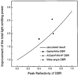
The LED improvement factor, defined as the ratio of the total light-emitting power of LEDs with DBRs and the light
output of LEDs without DBRs, is plotted against the DBR’s peak reflectivity as shown in Fig. 4. The line is the calculated result without considering the angle effect. The experi-mental results measured from LEDs with three different DBRs are shown by: 䊉 共GaAs/AlAs DBR兲, 䉱 共共Al0.4Ga0.6)0.5InP/AlInP DBR兲, 䉲 共the wide angle DBR兲.
Using the wide angle DBR, we have obtained an improve-ment factor of 2.55 with respect to those without DBRs. The reason that this value is higher than the calculated result is due to the wide angle reflection. This result is also much better than those obtained with conventional DBRs. With this wide angle DBR, the output power at 20 mA is about 2.1 mW and its quantum efficiency can reach 5.05%, compa-rable with wafer bonded AlGaInP LEDs with a very thick window layer.5We should point out that the process of
mak-FIG. 1. The calculated reflectivity as functions of light-emitting angle and wavelength for wide angle DBR with 15 pairs of共Al0.4Ga0.6)0.5InP/AlInP DBR and six pairs of GaAs/AlAs DBR.
FIG. 2. The simulated and measured reflection spectra for the wide angle DBR.
FIG. 3. The emission spectra of AlGaInP LEDs without DBR, with conven-tional DBR and with the wide angle DBR.
FIG. 4. The improvement on the total light-emitting power as a function of the DBR’s peak reflectivity.
2053
J. Appl. Phys., Vol. 87, No. 4, 15 February 2000 Chiouet al.
[This article is copyrighted as indicated in the article. Reuse of AIP content is subject to the terms at: http://scitation.aip.org/termsconditions. Downloaded to ] IP: 140.113.38.11 On: Thu, 01 May 2014 07:57:51
ing the proposed LEDs is the same as for conventional LEDs and it is much easier than making wafer bonded LEDs. Our result would be even better if a thicker window were used.
In conclusion, a wide angle DBR has been designed and implemented in conjunction with high brightness amber LEDs. In this design both the reflectivity and reflection angle of DBRs were considered. The light intensity of LEDs with the wide angle DBRs is about 2.55 times higher than that of the LEDs without DBRs. The output power at 20 mA is 2.1 mW and its quantum efficiency is 5.05%, which are compa-rable to those of wafer bonded LEDs with similar emitting wavelength.
The authors would like to thank W. Su for the EL mea-surements. This work is supported by the National Science Council under Contract No. NSC88-2215-E009-012.
1H. Sugawara, K. Itaya, and G. Hatakoshi, J. Appl. Phys. 74, 3189共1993兲. 2H. Sugawara, K. Itaya, and G. Hatakoshi, Jpn. J. Appl. Phys., Part 1 33,
6195共1994兲. 3
C. S. Chang, Y. K. Su, P. T. Chang, Y. R. Wu, K. H. Huang, and T. P. Chen, IEEE Photonics Technol. Lett. 9, 182共1997兲.
4K. H. Huang, J. G. Yu, C. P. Kuo, R. M. Fletcher, T. D. Osentowski, L. J. Stinson, M. G. Craford, and A. S. H. Liao, Appl. Phys. Lett. 61, 1045
共1992兲.
5
F. A. Kish, D. A. Vanderwater, D. C. DeFevere, G. E. Hofler, K. G. Park, and F. M. Steranka, Electron. Lett. 32, 132共1996兲.
2054 J. Appl. Phys., Vol. 87, No. 4, 15 February 2000 Chiouet al.
[This article is copyrighted as indicated in the article. Reuse of AIP content is subject to the terms at: http://scitation.aip.org/termsconditions. Downloaded to ] IP: 140.113.38.11 On: Thu, 01 May 2014 07:57:51