國
立
交
通
大
學
光電工程研究所
博 士 論
文
具超薄氧化層之記憶體與光伏元件
Memory And Photovoltaic Devices
With Ultrathin Oxide Layers
研 究 生:張 資 岳
指導教授:李 柏 璁 博士
具超薄氧化層之記憶體與光伏元件
Memory And Photovoltaic Devices
With Ultrathin Oxide Layers
研 究 生:張資岳 Student : Tzu-Yueh Chang
指導教授:李柏璁 博士 Advisor : Dr. Po-Tsung Lee
國 立 交 通 大 學
光 電 工 程 研 究 所
博 士 論 文
A Dissertation
Submitted to Institute of Electro-Optical Engineering
College of Electrical Engineering
National Chiao Tung University
in partial Fulfillment of the Requirements
for the Degree of
Doctor of Philosophy
in
Electro-Optical Engineering
October 2010
Hsinchu, Taiwan, Republic of China
i
具超薄氧化層之記憶體與光伏元件
學 生 : 張 資 岳
指導教授 : 李 柏 璁 博士
國立交通大學光電工程研究所 博士班
摘 要
在這本篇論文中,我們研究三個具超薄氧化層綠色電子元件,即兩個有機雙穩態元 件與一個金氧半太陽能電池。超薄氧化層除了可以幫助實現有機雙穩態的電阻態切換與 了解相對應的切換機制之外,也可以降低金半太陽能電池的逆向飽和電流而提升元件的 開路電壓。首先,我們研究具 n-type Si/Alq3/Al 結構的有機雙穩態元件特性。該元件的雙穩態 特性是主要來自 Alq3/Al 界面的缺陷態。值得一提的是我們可以藉由調控 Alq3薄膜沉積 鍍率去調整該元件的電性。為了瞭解這些現象,我們利用高解析電子能譜儀分析 Alq3 薄膜與 Alq3/Al 介面的化學組成,以及透過原子力顯微鏡與薄膜低掠角繞射解析 Alq3薄 膜與 Alq3/Al 介面的特性。
然 後 , 我 們 研 究 另 一 種 結 構 的 有 機 雙 穩 態 元 件 (p+-Si/Alq3/nanostructured MoOx/Alq3/Al)特性。該元件的雙穩態特性是來自嵌入於 Alq3薄膜內的 MoOx似奈米團簇 對載子捕抓與釋放之現象。當 MoOx似奈米團簇捕抓載子後(高導電態),所形成的空間
ii 電荷會主導元件內載子的傳輸機制。我們也探討該元件的雙穩態滯留時間與寫入-讀取-抹除-讀取之特性。 最後,我們提出一個有效提升開路電壓的疊合式金氧半太陽能電池結構,而該疊合 式金氧半太陽能電池是由一個 n 型金氧半太陽能電池與一個 p 型金氧半太陽能電池所構 成。在 AM1.5 模擬太陽光照射下,該太陽能電池的開路電壓可達 0.71V。該開路電壓高 於目前已發表的 n 型或 p 型金氧半太陽能電池之開路電壓。在此,我們成功地證明利用 疊合式金氧半太陽能電池結構提升太陽能電池的開路電壓之可行性。該疊合式金氧半太 陽能電池結構將在未來光伏元件應用於水裂解氫能中扮演重要的角色。
iii
Memory And Photovoltaic Devices With Ultrathin
Oxide Layers
Student: Tzu-Yueh Chang
Advisor: Dr. Po-Tsung Lee
Department of Photonics and Institute of Electro-Optical Engineering
National Chiao Tung University
Abstract
In this dissertation, we study three green devices using ultrathin oxide layers: two organic bistable devices (OBDs) and one metal-insulator-semiconductor (MIS) solar cell. The ultrathin oxide layers not only can help realize the resistance switching of the OBDs and recognize the corresponding mechanisms, but also can reduce the reversed saturation current of metal-semiconductor solar cells and thus can ameliorate the open-circuit voltage (Voc) of the solar cells.
First of all, the properties of an OBD using an n-type Si/Alq3/Al structure are investigated. The bistable effect of the OBD is primarily caused by the interface defects at the Alq3/Al interface. It is worthy to mention that the electrical properties of the OBD can be modified and controlled by utilizing the appropriate deposition rate of the Alq3 thin film. To
iv
understand these phenomena, we use high resolution X-ray photoelectron spectroscopy to analyze the chemical composition of the Alq3/Al interface and Alq3 thin films, and atomic force microscopy and grazing incident X-ray diffraction to characterize the properties of Alq3 thin films.
Furthermore, the electrical properties of an OBD with a p+-Si/Alq3/nanostructured MoOx/Alq3/Al structure are also investigated. The bistable switching of the OBD attributes to the charge trapping/erasing in the MoOx nanoclusterlike layer interposed between the Alq3 thin films. After charges are trapped in the MoOx nanoclusterlike layer (the high conductance state), the carrier transportation of the OBD will be dominated by a space-charge field which results from trapped charges. Both the retention measurement and write-read-erase-read cycles of the OBD are also provided.
Finally, a stacking MIS solar cell structure, which integrates an n-type MIS solar cell with a p-type MIS one, is proposed to effectively enlarge Voc. The measured Voc is up to 0.71V under simulated air mass (AM) 1.5 illumination (100 mW/cm2). This Voc is larger than those of the n-type or p-type MIS solar cells published. Here we successfully demonstrate the feasibility of the Voc enhancement of MIS solar cells by using a stacking structure. The stacking MIS solar cell will play an important role in photovoltaic application for hydrogen generation.
v
Acknowledgement
一路走來,有歡笑、淚水與辛酸,但不論我悲歡喜樂,父母親總是在身旁鼓勵著我, 使我不斷地向前邁進,如今我完成博士學業,最想跟我的父母親說:「爸、媽辛苦了!感 謝你們!」。 從碩士班一直到博士班,我皆在李柏璁教授實驗室做研究,李柏璁教授提供我多面 向的研究發展,也開啟我對於研究的思維,還有傳授寶貴的經驗,這些皆對於我的研究 有著莫大的助益;在我研究遇到瓶頸時,李柏璁教授總是盡全力地協助我,因而今天才 有這本論文的呈現,在此,感謝李柏璁教授多年來的指導與教誨,學生永遠銘記在心。 此外,還要感謝許多在我人生與學業上給予協助的老師們,因為有您們,我才能夠成長 更快、更茁壯。 在這幾年中,實驗室每年除了訓練有素的研究生畢業也有新的成員加入,因此結認 識許多學長、同學與學弟妹。感謝與我一起奮鬥的學弟妹們:思元、明璽、欣育、怡先、 光揚、又瑋、鈞隆、宜恒、書維、文齡與品睿等,能與你們一起打拼是我的榮幸,而實 驗室的其他成員:贊文、士強、吉東、紘鈞、國輝、鴻祺、書志、峻豪、豐懋、明峯、 俊德、佳禾、嘉銘、仲銓、孟穎、宜育、均融、和璁、韋德、逸華、青樺、佳揚、品佐、 君源、雋威、立勛、紹平等,雖然我們研究主題差很多,但是我從你們身上學到很多寶 貴的經驗,謝謝你們。 在我求學過程中,家裡姐姐們常常給予我適時的幫助與鼓勵,有妳們的關懷,我才 能更放心的在交大求學,感謝妳們。最後,感謝我可愛的女朋友:亭均,妳在這漫長的 時間裡,陪伴著我度過每一天,當我感到心情低落與迷網時,妳總是試圖讓我展開笑顏 與回復信心,有妳真好。 讀博士班雖然辛苦,但這是一種磨練,而當我遇見困難時,承蒙許多人的幫忙與照 顧,我才能順利走完攻讀博士之路;古人云:「施比受更有福!」,希望未來我是最有福 的人。 2010/10/27 于 新竹 國立交通大學 交映樓 401 室vi
Table of Contents
Abstract (Chinese) ... i Abstract (English)……….………...iii Acknowledgement ... v Table of Contents ... viFigure Captions ... viii
Table Captions ... xiii
Chapter 1 Introduction ... 1
1.1 Green Technology ... 1
1.2 Organic Resistive Memory ... 2
1.3 Solar Cells ... 10
1.4 Nano Films ... 16
1.5 The Motivation And Structure of This Dissertation ... 18
Chapter 2 Fabrication And Characterization Methods ... 20
2.1 The Fabrication of Organic Bistable Devices With Interfacial Oxide Layers ... 20
2.2 The Fabrication of Organic Bistable Devices With Nanostructured Oxide Layers ………...21
2.3 The Fabrication of Metal-Insulator-Semiconductor Solar Cells ... 22
2.4 The Fabrication of the Stacking Metal-Insulator-Semiconductor Solar Cell ... 24
2.5 Material And Interface Analyses ... 27
2.6 Device Characterization ... 31
Chapter 3 Organic Bistable Devices With Interfacial Oxide Layers ... 33
3.1 Organic Bistable Devices With Interfacial Layers ... 33
3.2 Results And Discussions ... 34
vii
Chapter 4 Organic Bistable Devices Using Metal Oxide Nanocluster Layers ... 45
4.1 Organic Bistable Devices Using Nanostructured Materials ... 45
4.2 Results And Discussions ... 46
4.3 Summary ... 53
Chapter 5 High Open Circuit Voltage Metal-Insulator-Semiconductor Solar Cells ... 54
5.1 A Stacking Metal-Insulator-Semiconductor Solar Cell ... 54
5.2 Results And Discussions ... 56
5.3 Summary ... 65
Chapter 6 Conclusions And Future Works ... 66
6.1 Conclusions ... 66
6.2 Future Works ... 67
References ... 69
viii
Figure Captions
Chapter 1
Fig. 1.1 The illustration of the three dimension (3D) stacking of ORM. ... 2
Fig. 1.2 4 types of I-V curves of OBDs. (a) Symmetric S-shaped. (b) Asymmetric S-shaped. (c) N-shaped. (d) O-shape. [8] ... 3
Fig. 1.3 The illustration of filamentary conduction. ... 7
Fig. 1.4 The illustration of nanoparticle/nanocluster charging.[66] ... 8
Fig. 1.5 The charge transfer between an Au NP and 8HQ.[64] ... 9
Fig. 1.6 The conformational change of the catenane.[76] ... 10
Fig. 1.7 The illustration of the main parameters of solar cells. ... 13
Fig. 1.8 The equivalent circuit of solar cells. ... 13
Fig. 1.9 The family of solar cells. ... 15
Chapter 2 Fig. 2.1 The structure of OBDs with interfacial oxide layers ... 20
Fig. 2.2 The fabrication flow of OBDs with interfacial oxide layers. ... 20
Fig. 2.3 The RCA cleaning process ... 21
Fig. 2.4 The structure of OBDs with nanostructured MoOx layers. ... 22
Fig. 2.5 The fabrication flow of OBDs with nanostructured MoOx layers. ... 22
Fig. 2.6 The fabrication flow of MIS solar cells ... 23
Fig. 2.7 The structure of the stacking MIS solar cell. ... 24
Fig. 2.8 The fabrication flow of the stacking MIS solar cell. ... 25
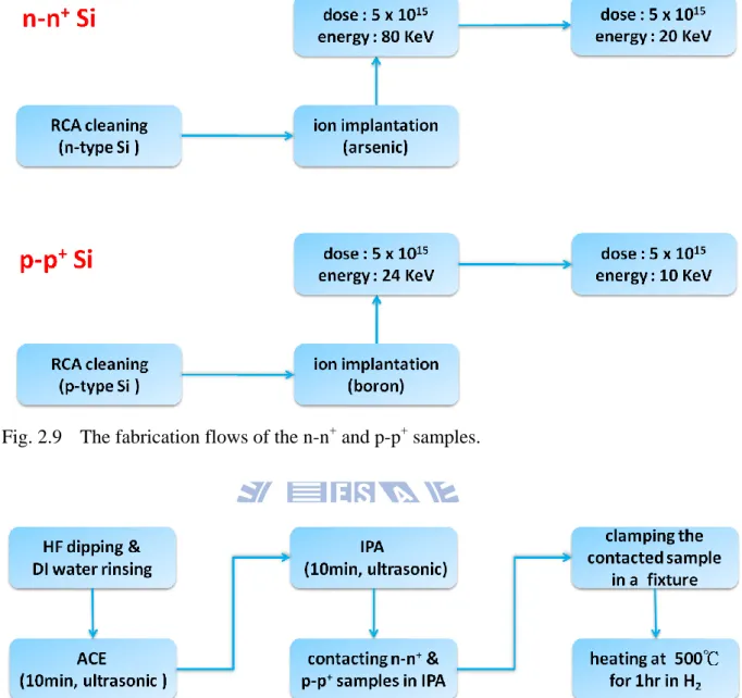
Fig. 2.9 The fabrication flows of the n-n+ and p-p+ samples. ... 26
Fig. 2.10 The flow of the bonding process. ... 26
ix
Fig. 2.12 The X-ray photoelectron process of HRXPS. ... 28 Fig. 2.13 The X-ray diffraction process. ... 29 Fig. 2.14 (a) The operation of AFM. (b) The forces between the AFM tip and the sample surface. ... 30 Fig. 2.15 The setup of the transmitted IR imaging system. ... 31
Chapter 3
Fig. 3.1 The I-V curves of the OBD with the n-type Si/Alq3/Al structure. The black square and red circle curves represent writing and reading biases, respectively. The inset shows the voltage-dependent ON/OFF current ratio curve. ... 35 Fig. 3.2 The reading currents after “writing” and “erasing” of the OBD with the n-type Si/Alq3/Al structure for the first four cycles. ... 36 Fig. 3.3 The linear I-V curve of the OBD with the n-type Si/Alq3/Al structure at the high conductance. ... 37 Fig. 3.4 The C-V curve of the OBD with the n-type Si/Alq3/Al structure at a frequency of 1 MHz. The Si electrode is kept at 0 V, and the bias on the Al electrode is swept form -5 V to 7 V. ... 38 Fig. 3.5 The XPS curves of the Al electrode and Alq3/Al interface of the OBD with the n-type Si/Alq3/Al structure... 38 Fig. 3.6 The electrical properties of OBDs with the n-type Si/Alq3/Al structure whose Alq3
thin films are deposited at different deposition rates: (a) the black square and red circle curves represent deposition-rate dependent threshold voltage, and deposition-rate dependent ON/OFF current ratios, respectively, and (b) threshold-voltage dependent retention time. Data points shown in (a) are average values measured from the OBDs. ... 39 Fig. 3.7 The AFM images of the Alq3 thin films deposited on n-type Si substrates at the four
x
different deposition rates. Surface roughness means are 0.38 nm, 0.35 nm, 0.31 nm, and 0.17 nm for deposition rates at 0.05 nm/s, 0.15 nm/s, 0.2 nm/s, and 0.3 nm/s, respectively. ... 40 Fig. 3.8 The GIXRD curves of the Alq3 thin films deposited at the four deposition rates. ... 41 Fig. 3.9 The illustration of the defect states in the Al-O compound layer: Elow and Ehigh. .... 42 Fig. 3.10 The temperature-dependent I-V curves of the OBD whose Alq3 thin film deposited at 0.05nm/s. ... 43
Chapter 4
Fig. 4.1 (a) The I-V curves of the OBD with the p+-Si/Alq3/nanostructured MoOx /Alq3/Al structure. The olive open squares, the red open circles, and the blue open triangles represent the writing, reading, and erasing sweeping biases, respectively. Inset: fitting of the I-V curve of the high conductance state in a log-log scale. (b) The I-V curves of an OBD with a p+-Si/Alq3/nanostructured MoOx/Alq3/Ag structure. The olive solid squares, the red solid circles, and the blue solid triangles represent the writing, reading, and erasing sweeping biases, respectively. Inset: The I-V curves of an OBD with a p+-Si/Alq3/Ag structure. The green half solid squares and magenta half solid circles are the first and second bias scans, respectively. ... 47 Fig. 4.2 The Al (2p) XPS curve of the Alq3/Al interface of the OBD with the p+-Si/Alq3/nanostructured MoOx/Alq3/Al structure ... 48 Fig. 4.3 The I-V curves of the p+-Si/Alq3/nanostructured MoOx/Alq3/Al structure. (a) With 3-nm-thick MoOx (b) With 8-nm-thick MoOx. ... 49 Fig. 4.4 The iIllustration of the writing and erasing processes of the OBD using a MoOx nanoclusterlike layer. ... 50 Fig. 4.5 (a) The surface morphology of the 5-nm-thick MoOx layer deposited on the p+-Si/Alq3. (b) The illustration of the effective fields of ordered and random dipoles.
xi
... 51
Fig. 4.6 (a) The retention measurement of the OBD with the p+-Si/Alq3/nanostructured MoOx/Alq3/Al structure. The red open squares and blue open circles correspond to the high and low conductance states. (b) The reading currents after writing and erasing of the OBD with the p+-Si/Alq3/nanostructured MoOx/Alq3/Al structure for the first eight cycles. The red solid squares and blue solid circles correspond to the high and low conductance states. ... 52
Chapter 5
Fig. 5.1 (a) The illustration of converting solar energy for hydrogen production using photovoltaics. (b) The clean, renewable energy cycle of solar hydrogen. ... 54 Fig. 5.2 (a) The J-V curves of MIS solar cells with and without H2 annealing under light illumination. (b) Corresponding C-V curves. All capacitance values are normalized by the largest value of each curve. ... 57 Fig. 5.3 The J-V curves of MIS solar cells with the fixed thicknesses of ultrathin sputtering SiO2 layers (n-type ~ 2 nm, p-type ~ 1 nm) deposited under different working pressures with H2 annealing under light illumination. ... 59 Fig. 5.4 (a) Voc and (b) C-V curves of n-type and p-type MIS solar cells with the fixed thicknesses of ultrathin sputtering SiO2 layers (n-type ~ 2 nm, p-type ~ 1 nm) deposited under different working pressures with H2 annealing. All capacitance values are normalized by the largest value of each curve. ... 60 Fig. 5.5 Energy band diagram and operation of the stacking MIS solar cell. ... 61 Fig. 5.6 The J-V curves of the stacking MIS solar cell with and without light illumination. Inset: The J-V curves of the optimized n-type and p-type MIS solar cells under light illumination. ... 62 Fig. 5.7 The IR images of the bonding interface of the stacking MIS solar cell (a) as-bonded
xii
stacking MIS solar cell. (b) RTA annealed stacking MIS solar cell. (c) Thinned stacking MIS solar cell. ... 64
xiii
Table Captions
Chapter 2
Table 2.1 The setting temperatures corresponding to the four deposition rates of Alq3 thin films, and the properties of the Alq3 thin films obtained from XPS measurements for the four deposition rates. ... 21
Chapter 5
Table 5.1 The measured parameters of MIS solar cells with and without H2 annealing. ... 58 Table 5.2 The measured parameters of MIS solar cells with the fixed thicknesses of ultrathin sputtering SiO2 layers (n-type ~ 2 nm, p-type ~ 1 nm) deposited under different working pressures with H2 annealing under light illumination... 59 Table 5.3 Voc comparison between the proposed stacking MIS solar cell and other MIS and MIS-IL solar cells. ... 63
1
Chapter 1
Introduction
1.1 Green Technology
Green technology has been largely developed recently for tackling environment and energy issues (such as the green house effect [1], [2]) which we are suffering. Green technology is the technology which uses less energy and generates less pollution. For example, we can modify our fabrication processes to be the clean, low-pollutant, and low-power ones (the environment-friendly processes).
Organic electronics (such as organic memory, and organic light emitting diodes) is one of main streams of green technology because of low temperature fabrication, low fabrication cost, light weight, and high mechanical flexibility. Due to growing demand in nonvolatile, rewritable memory of information technology in our daily life, organic resistive memory (ORM) has been paid much attention. It not only greatly reduces the fabrication processes and cost of conventional memory, but also is promising to solve the bottleneck of the scaling technology of the conventional semiconductor industry. Nevertheless, not enough efforts have been made to well response debates (such as the electrical performance, and the resistance switching mechanisms) yet.
Another main stream is green energy because of sustainable energy resources. It includes solar photovoltaics, solar thermal, wind power, biomass, water power, and geothermal. Solar photovoltaics, converting solar energy into electricity using solar cells, have much more potential in green energy because of less limitation factors such as assembly locations. However, many issues, such as the performance of solar cells, still have to be much
2
more concerned.
Nanotechnology has been widely investigated for decades and has become a mature technology nowadays. Applying nanotechnology in ORM and solar cells has potential to make both exhibit superior performance and to help us deal with the difficulties of both. It is also possible to help us realize more green devices, and thus, more green technology.
1.2 Organic Resistive Memory
With advancing progress in science and technology, the demands for more accurate simulations in research and for consumer electronic devices are increasing dramatically. Along with this trend, a tremendous demand for increased capacity of memory devices is also evident. In order to satisfy this current demand, the capacity of conventional memory devices (such as dynamic random access memory, and flash memory) has been augmented by scaling technology. [3] However, scaling technology will reach its physical limit in the near future. To overcome the scaling limit, various new memory devices such as single electron memory [4], spin memory [5], phase-change memory, [6] and ORM [7] have been investigated. ORM has attracted considerable attention due to superior characteristics: simple structures (e.g., electrode/organic material(s)/electrode), high-density integration (Fig 1.1), fast-writing/ erasing-operation speeds, and low-power consumption.
3
ORM is a memory device which has not less than two conductivities at the same applied voltage. For an organic bistable device (OBD), ORM with two conductivities, with a normally OFF/ON state, it holds at a low/high conductance state at the beginning when a writing bias is applied to it. It will change to a high/low conductance state as the bias passes a threshold voltage (or a set/reset voltage). When applied a reading bias, the device still holds at the high/low conductance state. It is obvious that this device exhibits two obviously different currents at the same applied voltage. In addition, the device can be switched back to the low/high conductance state again after an erasing bias (or a reset/set voltage) is applied to it. According to the electrical properties of OBDs have been published, the current-voltage (I-V) curves of OBDs can be roughly grouped into 4 types: symmetric S-shaped, asymmetric S-shaped, N-shaped, and O-shaped, as shown in Fig. 1.2. [8]
Fig. 1.2 4 types of I-V curves of OBDs. (a) Symmetric S-shaped. (b) Asymmetric S-shaped. (c) N-shaped. (d) O-shape. [8]
4
The resistance switching of insulating materials which is responsible to an applied bias above a certain threshold voltage (forming or electroforming) has been investigated since T. W. Hickmoot reported the resistance switching of Al2O3 in 1962. [9] Then, the resistance switching of insulating materials are also found in SiO, [10] ZnS, [11] and TiO [12] and polymeric insulators [13]. The resistance switching has attributed to the injection of metal ions from the electrodes (resulting in impurity bands in the insulators) [10], conducting filamentary pathways forming (from electrolytic processes [14], or the metallic electrodes [15]), carbonaceous material (from the insulator itself or sources introducing during fabrication [16]), and tunneling between metal particles/clusters produced during the electroforming process [17]. Although a number of published papers elucidate their results using the filamentary formation, the causes of the resistance switching have not been clearly understood so far.
The first report on the resistance switching of organic devices, which was found in the
glow-discharge-deposited poly(divinylbenzene) interposed between lead electrodes, was at 1968. [18], [19] Then the resistance switching were also observed in other glow-discharge polymers: styrene, [20], [21] acetylene, [21] benzene, [21] and aniline, [21] and in small organic molecules: tetracene [22], [23] and perylene [23]. Although investigation on the resistance switching had proceeded in past decades, the apparent progression was made after Ma et el. proposed a three-layer structure (organic/metal-nanocluster/organic) deposited between two Al electrodes. The organic layers are 2-amino-4,5-imidazoledicarbonitrile (AIDCN), and the metal-nanocluster layer (discontinuous metal nanoclusters) is introduced by evaporating a thin metal layer in the presence of oxygen or AIDCN. [24]-[27]
Up to now, the resistance switching has been demonstrated by numerous organic materials which can be classified into five categories: small molecules, polymers, donor-acceptor complexes, mobile-ion and electrochemical systems, and nano-particle (NP) blends. [28]
5
For small molecules, anthracene, [29] 9,10-bis-(9,9-diphenyl-9H-fluoren-2-yl) anthracene (DPFA), [30] pentacene, [31] aluminum tris(8-hydroxyquinolate) (Alq3), [32]-[35]
N,N‟-di(naphthalene-1-yl)-N,N‟-diphenyl-benzidine (NPB), [34] AIDCN, [36] molecules with
various acceptor groups for tuning ON/OFF ratios (such as 2,3-dichloro -5-6-dicyano-1,4-benzo-quinone (DDQ)), [37], [38] and squarylium dye Langmuir–Blodgett films [39] have been used as the active layers of ORM.
The active layers of ORM using polymers include insulators (like poly(butylme- thacrylate) (PBMA), [40] poly(ethylmethacrylate) (PEMA), [40] poly(methylmethacrylate) (PMMA), [40] polystyrene (PS), [35], [40], [41] and poly(vinylcarbazole) (PVK) [42]), conjugated polymers (like poly [3-(6-methoxyhexyl) thiopene] (P6OMe), [43], [44] poly[2-methoxy-5-(3‟,7‟-dimethyloctyloxy)-1,4-phenylene vinylene] (OC1OC10), [35] polyspirofluorene, [35] and poly[2-methoxy-5-(2‟-ethyl-hexyloxy)-1,4-phenylene vinylene] (MEH-PPV) [45]), copolymers (like poly(methylmethacrylate-co-9-anthracenyl-methylme- thacrylate) (MDCPAC) [46]), and small molecule/polymer multilayer structures using electrostatic self-assembly methods (like nickel phthalocyanine/poly(allylamine hydrochloride), [47] and Rose Bengal/poly(allylamine hydrochloride) [48], [49]).
The resistance switching of donor-acceptor complexes (DA complexes) results from charge-transfer induced by an applied electrical field. Potember et al. report the earliest resistance switching on Cu-tetracyanoquinodimethane (Cu-TCNQ). [50] TCNQ is the organic electron acceptor, and Cu can transfer electrons to TCNQ to from CuTCNQ (a charge transfer complex) when an electrical field is applied to the Cu-TCNQ thin film. Moreover, the resistance switching of organic-organic DA complexes (such as 2,6-bis(2,2-biscyanovinyl) pyridine (BDCP) and decacyclene (DC), [51] PVK and rare earth complexes (Sm3+, Gd3+, or Eu3+), [52] and poly(3-hexyl thiophene) (P3HT) and functionalized carbon nanotube (CNT) [53]), of DA complexes in a host polymer matrix (such as 6,6-phenyl-C61-butyric acid methyl ester (PCBM) and tetrathiafulvalene (TTF) in the PS host matrix [54]), and of DA
6
copolymers (such as a copolymer of europium vinylbenzoate complex (EuVB) and PVK, [55] a copolymer of 9,9-dihexyl-9H-fluorene-2,7-bis(trimethyleneboronate), 2,7-dibromo-9,9-di- hexyl-9H-fluorene, and 5,5‟-bis(5-(4-bromo-3,5-bis(2-ethylhexyloxy)phenyl)-1,3,4-oxadia- zol-2-yl)-2,2‟-bipyri-dine, [56] and a copolymer of EuVB and polyfluorene (PF) [57]) have been demonstrated as well.
In mobile-ion and electrochemical systems, ions in organic materials can be highly mobile. The external applied electrical fields can electro-deposite/de-solute the ions to generate/destroy the conducting paths (e.g., Cu ions coupling with Alq3, AIDCN, and 2,9,16,23-tetra-tert-butyl-29H,31H-phthalocyanine (ZnPc) [58]), can dissociate salts into ions to displace and/or accumulate (e.g., NaCl in polyphenylacetylene, [59] and sexithiophene-poly(ethylene oxide) (6T-PEO) adjacent with a poly(ethylenedioxythio -phene):poly(styrenesulfonate) (PEDOT:PSS) with a NaCl layer [60]), and can electrochemically oxidize/reduce the polymers with ions (e.g., a MEH-PPV/RbAg4I5 bilayer structure [61]), and then the resistance switching occur.
Nanostructured materials (such as metal NPs) have attracted much attention in ORM because the corresponding devices can exhibit better performance such as high ON/OFF ratios. The proposed nanostructured materials include Al discontinue nanoclusters, [24]-[27], [62], [63] Au NP blends (such as Au capped with triphenylphosphine (Au-TPP), [62] Au capped with dodecanethiol (Au-DT), [64]-[66] and Au capped with naphthalenethiol (Au-NT) [65], [67]), nanostructured Ag (such as Ag-ultrafine-particle–toluylene 2,4-dicarbamidonitrite (Ag-UFP-TDCN), [68] Ag NPs in a plasma polymer film, [69] Ag islands in N,N’-diphenyl-
N,N’-bis(3-methylphenyl)-1,1’-biphenyl-4,4’-diamine (TPD), [79] and a fine Ag layer in a
polyfluorene (PF) film with cyano side groups [71]), Pt NPs (such as Pt NPs into tobacco mosaic virus [72]), and other nanostructured materials (such as ZnO NPs, [73] MoOx NPs, [74] MoOx nanoclusters, [75]Cr NPs, [62] Mg NPs, [62] and CuPc NPs [62]).
7
ORM have been published, the physics responsible to the resistivity switching is not clearly known and largely debated. However, the primary proposed mechanisms include filamentary conduction, [33], [58] nanoparticle/nanocluster charging (charge trapping), [66], [75] charge transfer, [50], [64] and the conformation effects. [76], [77]
Filamentary conduction is a phenomenon that the current of a high conductance state is highly localized to a small fraction of the device area. When the devices are under electrical stress (or current stress), local fusing, the migration of electrode materials, or the alignment of NPs can form conductive filaments through the films, and thus the devices become at a high conductance state. These filaments can be ruptured by larger electrical stress (or current stress), and consequently the devices are switched back into a low conductivity state, as shown in Fig. 1.3.
Take a Cu-induced OBD (Cu (anode)/buffer layer/organic layer/Cu (cathode)) [58] as an illustration. Under a positive bias, Cu atoms close to the anode/buffer layer interface become ionized, and ionized Cu can drift into the organic layer and then towards the cathode. After they reach the cathode, Cu filaments are established within the organic layer, and therefore the organic layer is metalized (the high conductance state). When the applied bias exceeds a critical voltage which can break the Cu filaments via burning, the OBD change to the low conductance state again.
8
Moreover, filamentary conduction possess two features: (a) the current of the high conductance state will exhibit ohmic relation in I-V curves and will increase with decreasing temperature, and (b) the current of the high conductance state is independent on (or insensitive to) the device area in that the dimension of filaments is much smaller the device area.
Nanoparticles/nanoclusters can trap transporting carriers, and/or donate electrons or accept electrons under an (large enough) external electrical field. After them are charged to some extent, ORM will alter the pristine conductance state into another one as a result of trap-free, or a change in material properties (such as the electronic structure). Take a blended thin film which composes of Au-DT NPs in the PS [66] as an instance. The Au-DT NPs act as trap sites in the PS because the work function of the Au-DT NPs is around 5.1 eV lower than the lowest occupied molecular orbital of PS. When the film is applied a bias, its conductance is low initially due to charge trapping. However, as soon as the bias is larger than a voltage which the traps are completely filled, its conductance is largely enhanced, and the carrier transport mechanism is dominated by space charge limit current (SCLC), [78] as shown in Fig. 1.4. It should be noted that not only SCLC but also Poole–Frenkel emission, [79] Fowler–Nordheim [80] and direct tunneling [81] probably involve the carrier transport mechanism of the ORM using nanoparticles/nanoclusters.
9
A charge transfer effect is that a DA complex transits to an excited state in which a fraction of electronic charges is transferred between the donor to acceptor moieties. The resulting electrostatic force can either enhances or diminishes an external voltage applied to the devices. As a result, the devices can switch into a high or low conductance state. For example, a blended thin film consists of 8-hydroxyquinoline (8HQ) (electron donor), Au-DT NPs (electron acceptor), and PS (matrix). [64] Under an electric field, the carrier concentration of the blended thin film is quite low. However, as long as the electrical field increases to a certain value, electrons on the highest occupied molecular orbital (HOMO) of 8HQ can acquire enough energy to tunnel through DT into the Au NPs, as shown in Fig. 1.5. Therefore, the HOMO of 8HQ is partially filled, and the blended thin film is polarized. Then, the carrier concentration of the blended thin film is increased.
A conformation is defined as a possible shape of macromolecules corresponding to changes in their environment or other factors. A transition between the conformations is called a conformational change. A macromolecular conformational change may be induced by many factors such as electrical stress. Each conformation has its electrical conductance so the devices using macromolecules can alter their conductance under electrical stress. Take the catenane, [76] as shown in Fig. 1.6, for example. The catenane composes of a tetracationic cyclophane with two bipyridinium units, interlocked a crown ether with a tetrathiafulvalene
10
(TTF) unit and a 1,5-dioxynaphthalene ring system. The ground state of the catenane (“co-conformer” [A0]) has the TTF unit inside the cyclophane. After oxidation, the TTF unit is positively charged, and the Coulombic repulsion between TTF+ and the tetracationic cyclophane makes the crown ether circumrotate and then “co-conformer” [B+] is formed, which will reduce back to [B0] when the bias is returned to 0 V. The “co-conformer” [B0] can give larger output current than the “co-conformer” [A0]. The bistablity builds the basis of this device.
ORM is an emerging memory device and has many potential advantages. However, the electrical performance of ORM demonstrated so far cannot fit the requirements of next generation memory devices as well as the switching mechanisms are debated. For matching the requirements, improving the performance of ORM and making the responsible mechanisms clear are two key challenges of ORM. In addition, exploring emerging ORM based on nanomaterials, nanostructures, and/or low-cost fabrication techniques for the next generation green devices is always there.
1.3 Solar Cells
Solar cells are apparatus which can convert light energy into electrical energy. When Fig. 1.6 The conformational change of the catenane. [76]
11
sunlight illuminates into solar cells, photons larger than the bandgap of the active layer(s) are absorbed and then excited electron-hole pairs are generated. Before they relax to the ground state, the excited electron-hole pairs will be separated by a built-in asymmetry in the solar cells, and then the separated carriers are collected by electrodes. Finally, a potential difference (a photovoltage) between the electrodes which can drive electrons through external loads is generated.
The first report on the photovoltaic effect is that Edmud Bequerel observed an electric current generated by an Ag coated Pt electrode in the electrolyte under light illumination in 1839. In the following year, many kinds of solar cells were created (such as thin film Schottky barrier devices). With the development of silicon based solid state electronics in 1950s, the first pn junction silicon solar cell was made by D. M. Chapin, C. S. Full, and G. L. Pearson in 1954. [82] Its conversion efficiency is up to 6%. However, silicon solar cells were not widely applied in daily life for power generation at that time because of the high production cost, but in space. In addition, other type pn junction solar cells such as cadmium sulphide were also created in 1954, and many simulation works on solar cells using gallium arsenide, indium phosphide, and cadmium telluride were revealed as well. A big progress in solar cells occurred at the energy crisis in 1970s due to the huge amount of funding for research and development of alternative energy resources. As a result, new approaches for producing solar cells (such as photoelectrochemical junctions [83]) and cheap materials (such as polycrystalline silicon, [84] and amorphous silicon [85]), and for improving the performance of solar cells (such as multiple bandgap structures [86]) were intensively proposed. After the 1990s, not only the fabrication technologies of solar cells have been well developed, but the awareness on the sustainable energy resources and environment protection has been growing, and thus solar cells have been gradually expending into the electricity market. In order to accelerate the popularity of solar cells, high efficiency, low cost solar cells, and their applications (such as building integrated photovoltaic applications [87]) have greatly been
12
concerned.
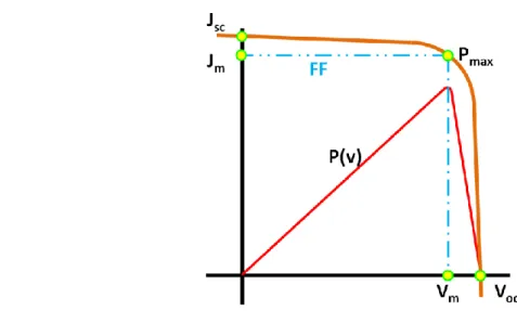
The current density-voltage (J-V) curve of a solar cell under illumination can be expressed by
(1.1)
where Jsc, Jo, q, n, kB, and T are short-circuit current density, reversed saturation current density, elementary charge, diode factor, Boltzmann constant, and temperature. The n is typically between 1 and 2. n approaches 1 as the diffusion current density of minority carriers dominates the carrier transportation mechanism. n approaches 2 as the recombination current density in the space charge region does. When two terminals of the solar cell are open-circuit (J=0), which the dark current density cancels out the Jsc, the potential difference between the two terminals is the open-circuit voltage (Voc), as expressed in Eq. (1.2).
(1.2)
Afterwards, when the solar cell connects with a load(s), the delivered power density is given by Eq. (1.3).
(1.3) The maximum delivered power density (Pmax) locates at some voltage (Vm) and a corresponding current density (Jm) in the J-V curve. The ratio of VmVm to VocJsc is defined as the filling factor, as given in Eq. (1.4).
(1.4)
The conversion efficiency of the solar cell (η) is the maximum delivered power as a fraction of incident power density (Pi), as expressed in Eq. (1.5).
η (1.5)
13
for describing its performance under a specific condition (e.g., the standard test condition: at 25℃, air mass 1.5 illumination (100 mW/cm2)).
A real solar cell always contains nonideal factors (e.g., parasitic resistance, and surface recombination) to dissipate its delivered power density. Take the parasitic resistance of the solar cell as an example. It comprises series resistance (Rs) and shunt resistance (Rsh), which are illustrated by Fig. 1.8 and which the corresponding J-V curve is expressed by Eq. (1.6). Rs results from the resistance of materials and the contact resistance in the interfaces (such as the metal-semiconductor contact). Rsh is introduced by leakage current paths (such as surface defects, and worse edge isolation). Rs makes influences on the Jsc but less on Voc. However,
Fig. 1.8 The equivalent circuit of solar cells.
14
Rsh behaves in opposite trend. Moreover, large Rs and small Rsh reduce the FF, and thus the potency of the solar cell. It suggests that an efficient solar cell ought to be with Rs as small and with Rsh as large as possible.
(1.6)
Current photovoltaic technologies can be categorized into three main groups: the silicon type, the compound type, and the new materials, as shown in Fig. 1.9. The silicon type includes bulk crystalline Si (single crystalline, [82], [84], [88]-[90] multicrystalline, [84], [91]-[94] and hetero-junction with intrinsic thin-layer [95], [96]), and Si thin films (single crystalline, [97], [98] multicrystalline, [99], [100] amorphous, [85], [101], [102] and multijunctions [103], [104]). Si is a chief material in solar cells due to its earth-abundance, non-toxicity, and stable oxide compounds, and to the well-developed Si based industry, although Si is an indirect bandgap material. In this type of solar cells, single crystalline Si gives the highest efficiency up to present. However, the production cost is also the most expensive. For reducing the cost, other Si based solar cells have been interested. Take amorphous Si thin film solar cells as an example, the absorption properties of amorphous Si thin films are superior to those of bulk Si, and consequently, material usage is largely reduced, which shifts to cut down the cost. The compound type comprises bulk crystalline III-V compounds (single junction, [105] and multijunction [86], [106-[108]), III-V compound thin films, [109], [110] II-VI compound thin films (such as CdTe), [111]-[114] and I-III-VI2 compound thin films (such as Cu(InxGa1-x)Se2 [115]-[118]). In all kinds of solar cells, single crystalline III-V compound solar cells are the champion cells nowadays (η with up to 40%). [107], [108] Comparing with crystalline Si ones, the cells consume less materials and assembly areas under the same output power. However, they are much more costly. With regards to II-VI and I-III-VI2 compound thin film solar cells, they have potential to compete with Si based photovoltaics as a result of their natures: direct bandgap materials (high
15
absorption coefficients), and flexibility in bandgap engineering. The new materials cover dye-sensitized solar cells (DSSC, thin film), [119]-[122] organic photovoltaics (OPVs, thin film), [123]-[127] and ultra high efficiency photovoltaics (such as quantum dots, [128] hot carriers, [129], multiband, [130], [131] and multiple excitation [131]). Both DSSC and OPVs are made of low-cost materials which can change their bandgaps by molecular engineering, and do not require elaborate apparatus for manufacturing; accordingly, are potentially lucrative for photovoltaic applications. Unfortunately, further investigation and improvement on their efficiency, stability, and strength are necessary for paving their roads on the photovoltaic market. In the case of ultra high efficiency photovoltaics, they attend to tackle power losses of solar cells (such as the thermalization loss [132]) for achieving over 31% Fig. 1.9 The family of solar cells.
16
efficiency (the efficiency limit of single junction solar cells [133]). Even if it is still early days, they manifest to have enormous potential in photovoltaic technology, possibly permitting more than two times obtainable cell energy conversion efficiency.
To take the place of nonsustainable energies (like fossil fuels, and uranium) in the near future, decreasing the capitalized cost of power converted by photovoltaics is our key challenges. Mass production, efficiency improvement (such as by new structure designs, new materials, and nanotechnologies), and novel photovoltaics (such as hot carrier cells) are much beneficial for lowering the cost. For example, uplifting 1% of the energy conversion efficiency of bulk single crystalline Si solar cells can cut down about 7% of the cost. [132] In addition, extending the applications of photovoltaics (such as BIPV and solar hydrogen) can also accelerate efficiently the popularization and developing of photovoltaics.
1.4 Nano Films
Nanotechnology is an applied science which studies the structures sized between 1 nm to 100 nm in at least one dimension. The corresponding thin films are nano films, which include films composed of nanocrystallites, [134], [135] composite films which nanocrystallites embedded in a film(s), [136], [137] 1 to 100 nm thick films, [138], [139] or multilayer films which 1 to 100 nm thick films stack in pairs. [140], [141] Because of their nature (the dimension of nanocrystalites, the thickness of films, surface roughness, and the structures of multilayers), numerous distinct physical or chemical properties of nano films [134]-[152] from bulk materials have been observed in mechanics, electronics, optics, and other research fields. For example, two ferromagnetic layers are separated by a very thin nonferromagnetic layer (e.g., Fe/Cr/Fe). The electrical resistance (magnetoresistance) of the structure is determined by the magnetization of the adjacent ferromagnetic layers (parallel or antiparallel alignment). It is interesting that the deviation of the magnetoresistance of the structure is extremely larger than that of conventional magnetic metals and alloys (giant
17
magnetoresistance). [142] Following is the brief introduction of part characteristics of nano films in electronics and optics.
In electronics, nano films can manipulate the behaviors of charge carriers. Four cases are given below.
(a) For crystallized particles or thin films, surface states which result from the broken periodic lattices at their surfaces can gradually change the pristine transportation behaviors of carriers when their dimension is decreasing, especially close to the range of the wavelength of electrons. For instance, the surface states can increase the charge storage time of a Si nanocrystal thin film. [144]
(b) A nano film(s) interposed between (composite) thin films can be trap states to catch carriers, and thus modulate the features of the (composite) thin films or corresponding devices. For example, a SiNx nano film, inserted between two SiO2 thin films, can act as the charge trapping centers of memory devices due to the energy barriers between SiNx and SiO2. [140]
(c) A particle with kinetic energy lower than the potential barrier of a thin film cannot penetrate the barrier until the thickness of the thin film is thin enough (e.g., SiO2 < 2nm), vastly different from the prediction of the classical physics. [135], [145]
(d) As the dimension of thin films is close to the Bhor radii of materials, continue energy states in the conduction band and valence band become discrete energy states. Then electrons can be largely injected into the thin films only if the Fermi level of the electrodes aligns with the discrete energy levels (Column blockade). [146], [147]
In optics, nano films can help mold the flow of light. Two examples are presented as follows.
18
(a) When electromagnetic (EM) waves pass through metal NP thin films, electrons on the metal NPs will oscillate with the EM waves, and then surface plasma is generated. As long as the frequency of EM waves are close to the resonance frequency of the metal NPs, localized surface plasma oscillation cause extensive light absorption. [148], [149]
(b) As the dimension of thin films shrink to make discrete energy states generate instead of continue energy states in the conduction band and valence band, we can observe blue shifts in the photoluminescence spectrum and absorption spectrum because of the enlargement of effective bandgaps. [137], [150]
Even though the dimension of nano films is far from that of bulk materials, nano films for some specific functions which are not provided by bulk materials can be easily fabricated using physical (such as sputtering) or chemical (such as synthesis) methods nowadays. For example, a nano film (or a nanostructured layer) can be the trapping layer of ORM for realizing the resistance switching. [75] Due to their promising characteristics, we can anticipate that applying nano films in ORM and solar cells will accelerate the progress of both, which in turn promote that of the green technology.
1.5 The Motivation And Structure of This Dissertation
Nano films have been widely applied in the numerous research fields because of their potential properties. In this dissertation, we use three kinds of ultrathin oxide layers (oxide nano films) to realize two OBDs and one solar cell for giving alternative solutions to the physical limit in the future scaling technology and for extending the functions of solar cells, respectively.
In the beginning, we fabricate and analyze an OBD with an n-Si/Alq3/Al structure, which an ultrathin Al-O compound layer forms unintentionally at the Alq3/Al interface. According to published results, the properties of interface oxide layers between the organic
19
layer and the electrode make influences on the characteristics of OBDs. In order to understand the effect of the ultrathin Al-O compound layer on our OBD, we investigate the characteristics of OBDs with the same structure made at different Alq3 deposition rates.
Moreover, we study an OBD using a nanostructured MoOx layer interposed by two Alq3 layers. The nanostructured MoOx layer can be trap sites to produce the resistance switching of the OBD under electrical stress due to the energy barrier between MoOx and Alq3. In organic electronics, MoOx has been extensively used to improve their performance. It suggests that the OBD can be easily integrated with other organic electronics.
In addition to the two OBDs, ultrathin oxide layers also play an important role on the photovoltaic features of Schottky solar cells. Inserting ultrathin oxide layers in the Schottky solar cells, metal-insulator-semiconductor (MIS) solar cells, can provide larger Voc under sunlight. MIS solar cells with high Voc appear a promising application, converting solar energy for hydrogen production, and can reduce the contact loss of photovoltaic modules. However, the Voc of MIS solar cells is not larger than the dissociating potential of water (1.23 V). A stacking MIS solar cell is proposed to further enhance Voc, and has potential to provide a Voc beyond 1.23 V.
This dissertation comprises six chapters. Chapter 1 gives the background and motivation of the studies. Then, the fabrication and characterization methods of samples are presented in Chapter 2. The following two chapters pay attention to the characteristics of an OBD with an interfacial oxide layer, and then involve the electrical features of an OBD with a nanostructured oxide layer. Materials in the Chapter 5 demonstrate a high Voc stacking MIS solar cell for a future photovoltaic application in water splitting. Finally, the conclusions and future works of this dissertation are summarized in Chapter 6.
20
Chapter 2
Fabrication And Characterization Methods
2.1 The Fabrication of Organic Bistable Devices With Interfacial Oxide
Layers
The OBDs consists of an Alq3 thin film interposed between n-Si and an Al electrode, as shown in Fig. 2.1. The fabrication procedures of the OBDs are described as follows and are illustrated in Fig. 2.2. First, 1 Ω-cm resistivity n-type silicon substrates were clean through the standard RCA cleaning process, as shown in Fig. 2.3. Then, 150-nm-thick Alq3 thin films were deposited on the cleaned substrates kept at room temperature by thermal evaporation in a vacuum below 3 x 10⁻⁶ Torr. Finally, 80-nm-thick Al top-electrodes were deposited on the Alq3 thin films through shadow masks. The area of each Al electrode is 0.64 mm2. The deposition rates of the Alq3 thin films are 0.05 nm/s, 0.15 nm/s, 0.2 nm/s, and 0.3 nm/s. The
Fig. 2.2 The fabrication flow of OBDs with interfacial oxide layers.
Fig. 2.1 The structure of OBDs with interfacial oxide layers
21
deposition rates are controlled by setting the temperature of crucibles and are monitored by the quartz crystal microbalance. The corresponding setting temperature for each deposition rate is listed in Table 2.1.
2.2 The Fabrication of Organic Bistable Devices With Nanostructured
Oxide Layers
The OBDs consist of an Alq3/MoOx/Alq3 tri-layer structure interposed between top and bottom electrodes, as shown in Fig. 2.4, and fabrication procedures are illustrated in Fig. 2.5. Table 2.1 The setting temperatures corresponding to the four deposition rates of Alq3 thin films, and the properties of the Alq3 thin films obtained from XPS measurements for the four deposition rates.
22
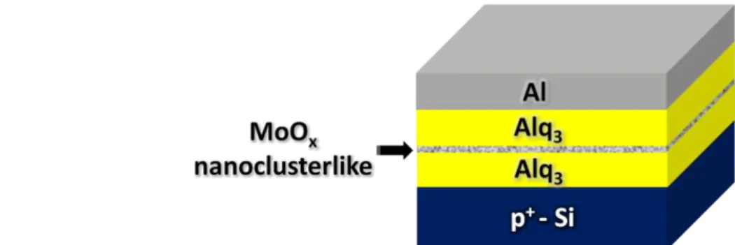
First, 50-nm-thick Alq3, XX-nm-thick MoOx, and 50-nm-thick Alq3 thin films were evaporated in sequence onto cleaned p+-type silicon substrates. The XX is equal to 3, 5, and 8. The average deposition rates of the Alq3 thin films and that of the MoOx layers are about 0.1 and 0.01 nm/s, which are monitored by the quartz crystal microbalance, respectively. Finally, 100-nm-thick Al thin films as the top electrodes were evaporated through metal masks with 2 mm x 2 mm square patterns. Note that all materials were evaporated at a vacuum bellow 3x10⁻⁶ Torr and the substrates were kept at room temperature during fabrication.
2.3 The Fabrication of Metal-Insulator-Semiconductor Solar Cells
The thickness of the insulating layers of MIS solar cells affects the blocking efficiency of their majority carriers and the tunneling probability of their excess minority carriers; hence, it influences their potency. Although thermal SiO2, [151]-[157] chemical SiO2, [158] evaporated SiOx, [159] and SiO2 using an anodization technique [160] have been used as their Fig. 2.5 The fabrication flow of OBDs with nanostructured MoOx layers.
.
Fig. 2.4 The structure of OBDs with nanostructured MoOx layers.
23
ultrathin insulating layers, controlling the thickness of the insulating layers well is still difficult to achieve. To easily control the thickness and to produce the insulating layers at the low temperature, radio frequency (RF) magnetron sputtering is adopted to deposit the ultrathin SiO2 layers.
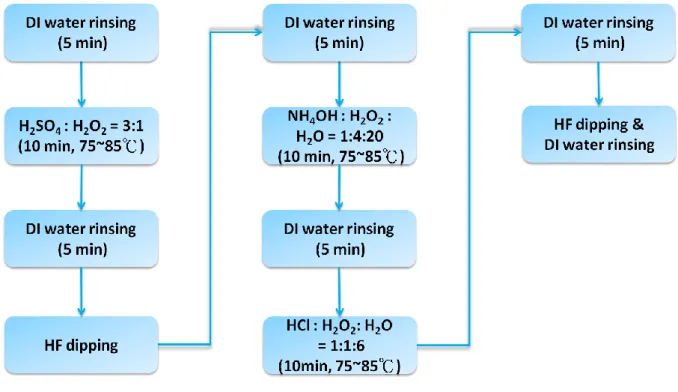
The n/p-type MIS solar cells were fabricated using phosphor/boron-doped (100) silicon substrates with resistivity ranging from 1 to 10 Ω-cm. The fabrication procedures are shown step by step in Fig. 2.6. First, ultrathin SiO2 layers were sputtered on n/p-type silicon substrates, which had cleaned through the standard RCA cleaning process, by RF magnetron sputtering under different working pressures. The thickness of the ultrathin SiO2 layers is controlled by sputtering duration. The optimized thicknesses for the n-type and p-type silicon substrates are about 2 and 1 nm, which the ultrathin SiO2 layers were sputtered at 20 mTorr, respectively. Thicker sputtering SiO2 insulating layers are required for the n-type MIS solar cells to suppress the larger tunneling probability of the majority carriers.
Then, most samples were annealed in H2 atmosphere at 500℃ for 1 hour, but the others are not for being reference samples. Finally, Al/Au(-Ni) films as the back electrodes, semi-transparent 20/10-nm-thick Au/Al thin film layers on the top of the ultrathin SiO2 layers, and Au(-Ni)/Al front finger electrodes were introduced by thermal evaporation. The area of all MIS solar cells is 0.2 cm2.
Fig. 2.6 The fabrication flow of MIS solar cells
24
2.4 The Fabrication of the Stacking Metal-Insulator-Semiconductor Solar
Cell
The proposed stacking MIS solar cell is composed of an n-type MIS solar cell as the top cell and a p-type MIS solar cell as the bottom cell with a tunneling junction in between. The structure is shown in Fig. 2.7, and its fabrication procedures are illustrated in Fig. 2.8. First, an n-n+ sample and a p-p+ one were fabricated using ion implantation and rapid thermal annealing (Sec. 2.4.1). Then, an n-n+-p+-p sample was prepared by bonding the n-n+ sample with the p-p+ one (Sec. 2.4.2). After the bonding process, both sides of the n-n+-p+-p sample were thinned by wet etching (Sec. 2.4.3). Since the n-n+-p+-p sample is too fragile for thickness measurement, the thicknesses are first roughly estimated by reference Si substrates using scanning electron microscopy. The thickness of the n-type Si substrate is about 90 μm and that of the p-type Si substrate is around 400 μm. The thickness of the n-type Si is designed to be much thinner than that of the p-type Si for current matching consideration. The optimal thickness for the n-type Si is about 4 μm. Finally, the sample was processed based on the optimized conditions obtained from the individual n-type and p-type MIS solar cells. The area of the stacking MIS solar cell is 0.2 cm2.
25
2.4.1 The Fabrication of the n-n+ and p-p+ Samples
The stacking MIS solar cell needs a tunneling junction which photoexcited majority carriers in the top cell can recombine with those in the bottom cell. Before forming the tunneling junction, an n-n+ sample and a p-p+ one are required. Following is the fabrication procedures of them, as shown in Fig. 2.9. First, n-type and p-type Si substrates were cleaned through the standard RCA process. Then the polished surface of the n-type Si substrate was doped with arsenic ions by ion implantation with doses of 5x1015 cm-2. The energy of ion implantation is 80 KeV and 20 KeV in sequence. Similarly, the polished surface of the p-type Si substrate was implanted with 24 KeV boron ions with a dose of 5x1015 cm-2 and then with 10 KeV boron ions with a dose of 5x1015 cm-2. The activation of the implanted ions, by rapid thermal annealing at 1050℃ for 10s, was executed after the bonding process.
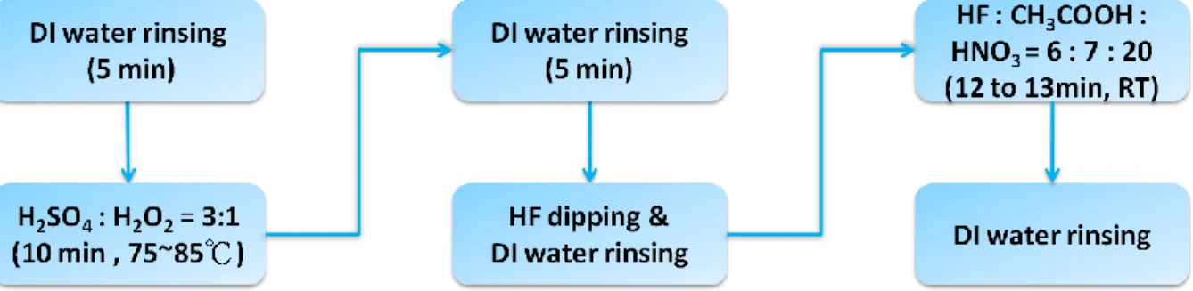
2.4.2 The Bonding Process
After obtaining the implanted samples, the n-n+-p+-p sample with a tunneling junction can be generated through a bonding process. The bonding procedures are disclosed below, as shown in Fig. 2.10. First, the implanted samples were dipped with a diluted HF solution and Fig. 2.8 The fabrication flow of the stacking MIS solar cell.
26
were rinsed with deionized (DI) water. Then, the samples were cleaned with aceton (ACE) and isopropanol (IPA) solutions in an ultrasonic cleaning tank in sequence. After the cleaning processes, the cleaned n-type sample was contacted directly with the cleaned p-type one in an IPA solution at room temperature, and then the contacted sample was fixed in the fixtures. Finally, the fixture was put into a heating chamber, and was heated at 500℃ for 1 hr in hydrogen atmosphere. The hydrogen can prevent the bonding interface from oxidation, which attributes to impurities in the chamber, during the heating process.
Fig. 2.10 The flow of the bonding process.
27
2.4.3 The Thinning Process
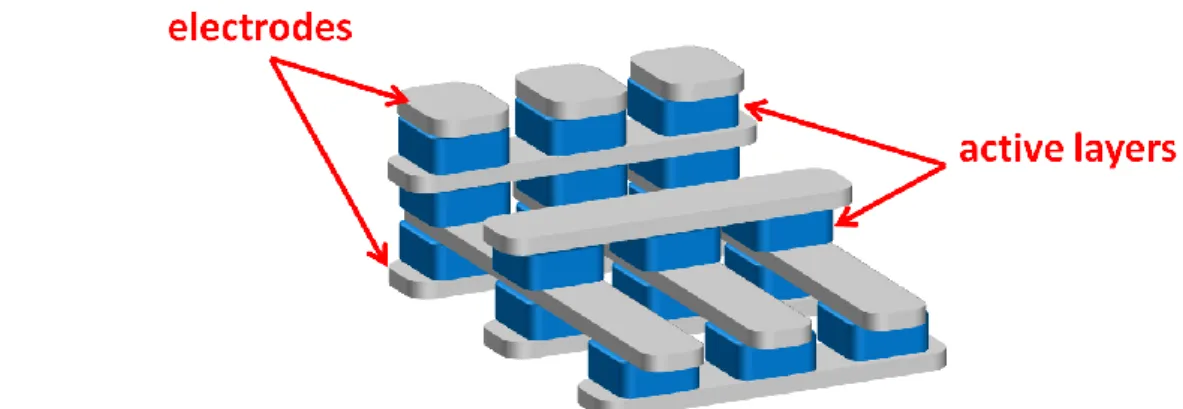
For balancing the photon fluxes of the top and bottom cells, the thickness of the top cell must be thinned toward the optimized thickness (4 m). The thinning process, as illustrated in Fig. 2.11, is revealed as follows. First, the well bonded sample was immersed in a etchant (HF : CH3COOH : HNO3 = 6 : 7 : 20) for 12 to 13 minutes. Finally, the etched sample was rinsed using DI water.
2.5 Material And Interface Analyses
2.5.1 High Resolution X-Ray Photoelectron Spectrometer
High resolution X-ray photoelectron spectroscopy (HRXPS) can help deduce the chemical composition of materials on the surfaces. When monoenergetic soft X-rays with photon energy hν irradiated by solids in vacuum illuminate on the surface of a material, photoelectrons with kinetic energy Ekin will emit out of the surface and are collected by the analyzer, as shown in Fig. 2.12. The spectrum is a plot of the number of emitted photoelectrons per energy interval versus their binding energy Eb, as expressed by Eq. (2.1).
(2.1) The composition of the Alq3/Al interfaces and the atomic concentration of the Alq3 thin films were analyzed by measuring the Al-2p, and N-1s and O-1s photoelectron spectra, respectively, using HRXPS (ULVAC-PHI Quantera SXM) after Ar+ milling on the sample surfaces. The HRXPS equips with a monochromatic Al Kα radiation X-ray source and
28
a hemispherical energy analyzer. The power of the X-ray source is 25 W at 15 kV accelerating voltage, and the analyzed area of the samples is about 100 μm2.
2.5.2 Grazing Incident X-Ray Diffraction
X-ray diffraction is a nondestructive approach to identify the crystallization structures of solids. For a sample with regular arrays of atoms, the atoms will scatter the waves when X-ray waves illuminate into the sample, as shown in Fig. 2.13. Diffraction patterns can be obtained as long as the phases of not less than two scattering waves superposition to meet Bragg‟s law, as expressed by Eq. (2.2), where d is the spacing between diffracting planes,
θ
is the incident angle, n is any integer, and λ is the wavelength of the X- ray beam. According to a plot of diffraction intensity verse diffraction angles, the crystallization structures of the sample can be identified.λ (2.2) The structural information of the Alq3 thin films deposited at different deposition rates was analyzed via XRD (Rigaku, RU-H3R) using a grazing incident X-ray diffraction (GIXRD) mode. The incident X-ray was fixed at a tiny angle with respect to the surfaces of the Alq3 thin films, and the detector did 2θ scan.
29
2.5.3 Atomic Force Microscope
Atomic force microscope (AFM) is an apparatus whose primary component is an extremely sharp tip mounted or integrated on the end of an extreme small cantilever spring which is moved by a mechanical scanner over the surface of a sample, as shown in Fig. 2.14(a). AFM can provide the topography of bare and monolayer coated solids. When the tip is moved close to a sample surface, forces between the tip and the sample surface can result in a deflection of the cantilever owing to Hooke's law. According to the deflection detected by a laser beam, the morphology of the sample surface can be obtained. For conventional AFM, two operation modes are available, the contact mode (the tip onto the sample surface, repulsive force) and the tapping mode (the tip in close vicinity of the sample surface, attractive force), as shown in Fig. 2.14(b).
The surface morphology of the Alq3 thin films on the Si substrates and that of the MoOx layers on the Alq3 thin films were obtained by using AFM (DI-Veeco Instruments, D3100). We chose the tapping mode to scan the sample surfaces because of the softness of organic thin films.
30
2.5.4 Transmitted Infrared Imaging System
The bonding interface of the stacking MIS solar cell plays an important role in the performance of the stacking MIS solar cell because the interface is where the majority carriers of the top cell recombine with those of the bottom cell. If the interface cannot be a good tunneling junction and/or is not well bonded, the Voc enhancement of the stacking MIS solar cell will be blocked. In order to observe the interface, a transmitted infrared (IR) imaging system, which consists of a light bulb, a sample stage, a focus lens, an IR charge coupled device (CCD), and a screen, as shown in Fig. 2.15, was established.
The operation of the system is presented as follows. When photon fluxes, emitted from the light bulb, are incident into the bonded sample, photons with energy larger the bandgap of Si (1.124 eV) are absorbed by the bonded sample. The rest photons, whose energy less than 1.124 eV, are detected by the IR CCD. If any unbonded area (interface bubbles or voids) generates in the interface, fringe patterns, which result from the interference of the passing IR photons, can be observed on the screen.
Fig. 2.14 (a) The operation of AFM. (b) The forces between the AFM tip and the sample surface.
31
2.6 Device Characterization
2.6.1 Current-Voltage Measurement
The I–V curves of OBDs (the writing process, the erasing process, the reading process, the retention test, and the write-read-erase-read cycle) were measured in an ambient environment using a measurement system which is composed of a personal computer, a Hewlett Packard 4156A semiconductor parameter analyzer, a switching box, and a probe station. The writing bias, the erasing bias, and the reading bias are sweeping voltages and/or (quesi-)pulse voltages.
2.6.2 Capacitance-Voltage Measurement
A measurement system which includes a personal computer, an Agilent 4284A Precision LCR meter, a switching box, and a probe station was adopted to record the high frequency capacitance-voltage (C-V) curves of OBDs and MIS solar cells.
32
2.6.3 Photocurrent Measurement
The J-V curves of MIS solar cells were obtained using a solar simulator system which consists of a laptop, a Keithley 2400 source-measure unit, a probe station, and a solar simulator with an Air Mass 1.5 source with a power of 100 mW/cm2 (Oriel Class A). The illuminated light intensity was calibrated by a polycrystalline silicon solar cell certified by the National Renewable Energy Laboratory (NREL).
33
Chapter 3
Organic Bistable Devices With Interfacial Oxide
Layers
3.1 Organic Bistable Devices With Interfacial Layers
Interface layers between the (metal) electrodes and organic layers of OBDs play an important role in the characteristics of organic electronics. [161] For understanding the interface effects on OBDs, some have paid attention on the interface engineering of OBDs. [35], [161]-[166] Kondo et al. demonstrate that the ON/OFF ratio of OBDs is significantly enhanced by modifying the ITO electrodes (introducing Ag nanodots between the organic layer and the indium tin oxide surface). The Ag nanodots act as trapping sites, reducing the current of the OFF state. [162] Cho et al. form a self-assembled monolayer (4-nitrophenyl dichloride phosphate) on the hydroxyl-terminated Al electrode surface with native oxide to enhance switching reproducibility with an improved current level distribution. [163] Moreover, when an aluminum electrode is deliberately oxidized or unintentionally is passivated with native oxide, some organic devices display written, reproducible resistance switching. [35], [164]-[166] Cölle et al. show that the switching mechanism of OBDs with a (metal) electrode/organic/(metal) electrode structure (at least one electrode using Al) is due to the oxide layer on the Al electrode, and carriers transport through filaments, whereas the organic materials have only minor influences on it. [35] Verbakel et al. realize reproducible OBDs by deliberately adding thin sputtering Al2O3 layers to the surfaces of the bottom electrodes of nominal electron-only, hole-only, and bipolar organic diodes. They attribute the operation of the OBDs to the soft breakdown of the sputtering Al2O3 layers. In addition, the
34
OBDs exhibit negative differential resistance (NDR) and local maximum currents in the I-V curves, which are dependent on the thickness of the sputtering Al2O3 layers. In their case, the polymers play a role as a current limiting series resistance. [165] Cho et al. study OBDs with a interfacial AlOx layer, using an O2 plasma treatment method, formed on the surface of the bottom Al electrode. The OBDs give higher ON/OFF ratios than those without the interfacial AlOx layer because of the relatively small resistance at the OFF states. Nevertheless, the duration of the O2 plasma treatment makes a great influence on the threshold voltage distribution and the switching reproducibility. [166]
In this chapter, an OBD with Alq3/Al deposited on an n-type Si substrate, as shown in Fig. 2.1, is fabricated and investigated. The OBD shows distinct bistability with an ON/OFF current ratio over 106 and a wide reading voltage range for differentiating between „„ON” and „„OFF” states. The formation of electrically bistable states is the result of electrons being trapped in the defects at the Alq3/Al interface during electrical field stressing. This study also provides a simple approach, varying the deposition rate of the Alq3 thin film, using which the electrical characteristics of the OBD, e.g., threshold voltage, can be tuned or controlled. HRXPS, AFM, and GIXRD measurements are performed to help us understand the properties of Alq3 thin films and the Alq3/Al interface and explain the experimental results obtained. Besides, the simple structure of the OBD indicates that the OBD can be easily embedded into the well-developed semiconductor fabrication processes.
3.2 Results And Discussions
Figure 3.1 shows typical I-V curves of the fabricated n-type Si/Alq3/Al structure. As can be seen, this device exhibits two different conductance states at an identical applied voltage. The silicon electrode is kept at 0 V, and all bias conditions are applied on the aluminum electrode. At the first bias (the black square curve in Fig. 3.1), the voltage sweeps from 0 V to 10 V. Initially, the device exhibits a low conductance state (OFF state). However,
![Fig. 1.4 The illustration of nanoparticle/nanocluster charging. [66]](https://thumb-ap.123doks.com/thumbv2/9libinfo/8229444.170853/23.892.145.757.861.1069/fig-illustration-nanoparticle-nanocluster-charging.webp)
![Fig. 1.5 The charge transfer between an Au NP and 8HQ. [64]](https://thumb-ap.123doks.com/thumbv2/9libinfo/8229444.170853/24.892.132.642.869.1068/fig-charge-transfer-au-np-hq.webp)