Numerical Study on Thickness Dependence of Passivation Layer in
Top-Emission Organic Light-Emitting Device
Chia-Chiang Shiau
a, Hung-Chi Chen
a, Jiun-Haw Lee
a, Yean-Woei Kiang
a, C. C. Yang
a, and
Chih-Hsiang Chang
ba
Graduate Institute of Communication Engineering, Graduate Institute of Electro-Optical
Engineering, and Department of Electrical Engineering, National Taiwan University, No. 1, Sec.
4, Roosevelt Road, Taipei, Taiwan, R.O.C.;
b
Material Research Laboratory, Industrial Technology Research Institute, No. 195, Sec.4, Chung
Hsing Rd., Chutung, Hsinchu, Taiwan 310, ROC
ABSTRACT
In this paper, we demonstrate simulation results of a top-emission organic light-emitting device (TOLED) with a passivation layer and a dielectric layer. Passivation layer is usually composed of silicon dioxide (SiO2) and/or silicon
nitride (Si3N4) to protect organic layers from oxygen and moisture. Dielectric layer is a high refractive index thin
film for enhancing the external quantum efficiency. The TOLED device has a microcavity structure which comprised of an opaque and high reflective anode and a thin semitransparent cathode. When varying dielectric layer thickness, the output intensity changes and the spectrum peak shifts. The peaks oscillate as a function of the dielectric thickness and the period is around hundreds of nanometers depending on the refractive index of the dielectric layer. When adding the passivation layer, which is on the order of micrometers, more than single peak are observed. With a simple model, we found that the frequency difference between two peaks corresponds to the free spectral range of the fabry-perot cavity formed by passivation layer. When a passivation layers is added on the TOLED, the microcavity effect results in the presence of multi-peaks. It limits the view angle and decreases the color purity.
Keywords: OLED, optical simualtion.
1. INTRODUCTION
OLED is one of the most promising candidates for the next generation display technologies since it exhibits advantages such as self emissive, wide-view-angle, flexible-substrate-capability and potentially low cost [1],[2]. However, there are still several problems concerning the stability and the lifetime. Typically, such a device consists of an indium-tin-oxide (ITO) anode, a p-type and n-type organic layers, and a metal cathode. Electro-luminescence (EL) is generated from the organic layers and coupled out of the device from the ITO side. To drive devices in a display, passive matrix (PM) and active matrix (AM) techniques were used. Although the cost is lower, PM architecture require high peak drive currents to provide high peak luminance, which results in higher power consumption along with adverse effects on the OLED reliability. On the other hand, AM technique is more suitable for the large size, high quality and long lifetime applications. However, the thin-film transistor (TFT) on the AM backplane decreases the aperture ratio of a pixel that decreases the emission efficiency. Top-emission OLED (or TOLED) is one of the most promising technology for achieving high aperture ratio active matrix OLED. However, the fabrication process and the optical design of such a device is quite different from the conventional bottom-emission OLED. TOLED has an optical resonator with coplanar reflectors separated by a distance on the order of the optical wavelength. The reflectors contain the high reflective anode and semitransparent metal cathode.
It causes the spectral and spatial emission narrow significantly, and the forward emission intensity is enhanced [3]. The organic molecular used in OLED are very sensitive to moisture and oxygen, and the oxidation metal electrode will cause damage to the device. To achieve long lifetime and stability, it is necessary to cap a passivation layer on OLED device to protect organic materials and cathode from oxygen and moisture. Typically, the inorganic layer (like SiON) or organic layer is fabricated to serve as the passivation layer. However, it is not enough to protect
the OLED device from oxygen and moisture when only using a single thin film. Thus, multilayer passivation layers composed of polymer and inorganic barrier layers are use to serve as the function of passivation stress relaxation, respectively [4]. Usually, the thickness of the passivation layer is about several micrometers. It is composed with SiON with a refractive index of 1.4. The structure usually needs three pairs to protect device from moisture and
oxygen efficiently. On the other hand, because the EL from the TOLED passes through the passivation layer, the EL characteristics will be changed by the passivation layer. Here, we use an electromagnetic theory model to simulation the optical characteristics of TOLED with passivation layer. Our results indicate that both the efficiency and the color spectra of TOLED vary strongly with the thickness and materials of the passivation layer. The variation in efficiency and color can be explained by fabry-perot cavity effects of thick passivation layer. The theory details are represented in section 2. The results and the related discussions are shown in section 3. Conclusions are drawn in section 4.
2. THEORY
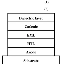
The TOLED device consists of multilayer structure as shown in Fig.1. The devices are fabricated on glass substrate with an opaque anode Ag. The organic multilayer structure consists of 60nm N,N´-dipheny1-N,N´-bis(1,1´-bipheny1)-4,4´-damine (NPB) as the hole-transporting layer (HTL), 60nm tris-(8-hydroxyquinoline) aluminum (Alq3) as the electron-transporting layer (ETL) and emitting layer (EML). The EL is observed through a semitransparent metal cathode consists of 20nm Ag. Finally, a dielectric layer such as ZnSe was added to enhance the output coupling efficiency. To understand the physical mechanisms of the radiation from an OLED, we need first to derive the governing equations for electric and magnetic field in each layer of the device. We assume the electrons and holes recombine and form excitons at the HTL and ETL interface. The excitons in the emission layer can be represented as oscillating dipoles. For calculating the radiation from dipole sources embedded in the emission layer (EML), we first introduce the electric Hertzian vector potential due to a vertical or horizontal dipole embedded in the EML[5], [6], [7] , [8]. Then, with ej tω time-harmonic dependence, the electric and magnetic fields can be derived from the Hertzian vector potential.
2 2 0 E=k n ∏ +∇∇ ⋅ ∏ (1) 2 0 H= −jωε n ∇ × ∏ (2) Substrate Anode EML Cathode Dielectric layer HTL
where n is the complex refractive index and k0 =ω µ ε0 0 =2 /π λ is the wave number or propagation constant in vacuum. The wave equations for Π can be expressed as
(
2 2 2)
0 0 i n k ∇ + ∏ = , in ith (non-emission) layer (3)(
2 2 2)
0 2 0 ( ) e e p r r n k n δ ε ′ − − ∇ + ∏ = , in EML (4)where p denotes a dipole source which is located at r=r´ and ne is the wavelength-dependent complex refractive
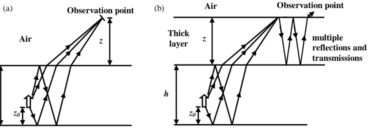
index for the EML. We employ the property of axial symmetry and take the Fourier-Bessel transform to obtain an integral expression for the Herzian vector potential in each layer of OLED. By using the boundary conditions that the tangential electric and magnetic fields are continuous across the interface between layers, we can determine the unknown coefficients in the integral expression of Hertzian potential from which all the electromagnetic field components can then be calculated accordingly. To calculate the radiation field in the far region, the saddle-point method (as shown in Fig. 2(a)) is usually used to perform the integration over the radial wavenumber [9]. If the outside layer is very thick, such as glass substrate in bottom emission OLED, we safely employ the saddle-point method to determine the mathematical expression of the radiation field E at the original interface between the air region and the outside layer (as shown in Fig. 2(b)). Then the radiation field E, acting as an incident field in the glass layer, will propagate in thick layer subjected to multiple reflections and transmissions. Employing the electromagnetic theorem with matrix multilayer enables us to evaluate the effective impedance ηeff of the multilayer structure below the glass layer to the glass layer. Let us first use the Fresnel formula to evaluate the reflection coefficient Γ2 from the glass layer to the multilayer structure, and the reflection coefficientΓ1 and the transmission
coefficient T1 from the glass layer to the air region. Then we can determine the effective transmission coefficient Teff
for Eglass to transmit to the air region.
0
1
2 sec
1 2
1
glass glass glasseff jk n d
T
T
e
− θ=
− Γ Γ
(5)
Note that the radiated field in the thick outside layer E is not a plane wave but a spreading beam wave. Using the principle of energy conservation and Snell’s law, we can derive a multiplicative spread factor.
1 2 2
cos
1 (
sin
)
air air glass air air glassn
S
n
n
n
θ
θ
=
−
(6)
where Θair is the refractive angle from the glass layer to the air region.
The above procedure is applicable to either a vertical dipole source or a horizontal one. The radiation, field due to a horizontal or vertical dipole source embedded in the emission layer can finally be expressed as
/ / / / / / ( 7 ) ( 8 ) ( 9 )
ˆ
ˆ
a i r g l a s s e f f a i r g l a s s e f f a i r a i r a i rE
E
T
S
E
E
T
S
E
p E
s E
⊥ ⊥ ⊥=
×
×
=
×
×
=
+
r
where Teff⊥ and Teff∥ are the effective transmission coefficients for the perpendicular and parallel polarizations, respectively.
For a dipole source operating at a single frequency, strong interference of the coherent fields reflected from interfaces between layers results in a rapidly oscillatory radiation patter. The oscillatory phenomenon in the radiation patter becomes more severely especially when the thickness of the glass layer is much larger then the wavelength. In fact, every real light source should have a finite bandwidth and the interference will be smoothened. Therefore, we assume that the dipole source is of a finite bandwidth, and the resultant radiation field is obtained by coherently averaging the fields over that range of wavelengths.
3. RESULTS AND DISCUSSIONS
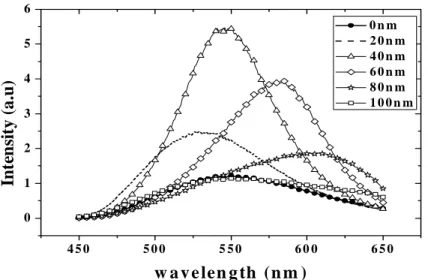
As shown in Fig. 1, a TOLED was deposited with a dielectric layer on top of a semitransparent metal cathode to enhance the output coupling. The dependence of the EL intensity emitted in forward direction versus the dielectric thickness is illustrated in Fig. 3. The EL spectrum first blue-shifts then red-shift and the EL intensity also has a increase followed by a decrease with increasing the dielectric layer thickness. When dielectric layer is 100nm, we can see that the EL spectrum is nearly the same as there is no dielectric layer. The EL spectrum changes with the dielectric layer thickness that has a period of 100nm. It can be calculate from a simple equation, 2nd/λ=mπ, where n is the refractive index, d is the dielectric layer thickness, λ is the wavelength, and m is an integer. We also found that the spectrum has blueshift with increasing the viewing angle. From Fig. 4, we can see that the different dielectric materials with distinct refractive index exhibit different oscillating behaviors. The higher refractive index material has larger oscillating amplitude and shorter period.
multiple reflections and transmissions h z Observation point Thick layer (b) h z Observation point (a) Air z0 z0 Air
Fig. 3 Simulation results of EL spectrum (at viewing angle=0°) with various dielectric layer thickness. OLED structure: Ag/ 60nm NPB/ 60nm Alq3/ 20nm Ag/Xnm dielectric layer (refractive index=2.6).
Fig. 4 Simulation results of intensity (at wavelength =500nm, viewing angle=0°) as a function of different dielectric layer refractive indices and different dielectric layer thickness. OLED structure: Ag/ 60nm NPB/ 60nm Alq3/ 20nm
Ag/Xnm dielectric layer.
Figure 5 illustrates the EL intensity of TOLED change versus different dielectric layer thickness with different OLED layer structures. Typically, we set the emission zone is located at the interface of NPB/Alq3. However, we intentionally shift the emission dipoles into the Alq3 layer and monitor the optical characteristics. As shown in Fig. 5, when change the dipole position, it only changes the output intensity of the EL spectra are similar. On the other hand, with increasing the thickness of Alq3 layer, the relative intensity of the same dielectric layer decreases, and the peak position shifts. Besides, the EL spectrums change obviously with different device structure. In fact, this can be explained by using the planar microcavity effects.
4 5 0 5 0 0 5 5 0 6 0 0 6 5 0 0 1 2 3 4 5 6
Int
en
si
ty
(
a
.u)
w a v e len g th (n m )
0 n m 2 0 n m 4 0 n m 6 0 n m 8 0 n m 1 0 0 n m 0 5 0 1 0 0 1 5 0 2 0 0 0 .5 1 .0 1 .5 2 .0 2 .5 3 .0 3 .5 4 .0 4 .5 5 .0In
te
n
sit
y (
a
.u
)
d ielectric la y er th ick n ess (n m )
n = 1 .4 5 n = 1 .8 n = 2 .2 n = 2 .6
2 2 2 2 1 2 2 1 1 1 i eff up out in i eff T r e E E r r e ϕ Φ × + = × − (6)
where Eoutup 2 is the output intensity, Ein 2 is the intensity of emission dipoles, r1 is the reflectivity of NPB to
anode, reff and Teff are the effective reflectivity and transmission of Alq3 pass through the layer composed of the
cathode and dielectric to the air, respectively. The symbol φ is the optical length of total organic layer, and Φ is the optical length between the dipoles and anode. The output intensity is affected by these two factors, the total organic layer thickness and the position of the emission dipoles. We can see that the periods in Fig. 5 are not affected by the total thickness of the organic layer. It is determined by the dielectric material. The output intensity of the five cases in Fig.5 is different. With increasing the thickness of the EML, the intensity decreases since the denominator of equation (6) is smaller in a thinner device within our simulation range.
Fig. 5 Simulation results of intensity (at wavelength =500nm, viewing angle=0°) as a function of different dipole position and EML thickness. Device A: Ag/ 60nm NPB/ 60nm Alq3/ 20nm Ag/Xnm dielectric layer. DeviceB: Ag/
60nm NPB/ 40nm Alq3/ 20nm Ag/Xnm dielectric layer. Device C: Ag/ 60nm NPB/ 80nm Alq3/ 20nm Ag/Xnm
dielectric layer.
Fig. 6 shows the EL intensity of TOLED versus cathode thickness with varying dielectric layer thickness. We can see that the intensity is strongly influenced by the cathode and dielectric layer. With increasing the thickness of cathode, the output is typically decreased due to the strong absorption of the metal cathode material. That means the cathode thickness should be thinner. However, in experiments the metal cathode is necessary and the thickness should be thicker than 20nm for forming a continuous film and efficient conductivity. When cathode is 0 nm and the dielectric layer thickness is varied, the intensity shows an oscillating behavior as shown above. When the cathode thickness is fixed at 20nm, we can see that the optimized dielectric layer thickness is 30nm to achieve highest intensity. 0 50 100 150 200 0.0 0.5 1.0 1.5 2.0 2.5 3.0 3.5 4.0 4.5 5.0 5.5
In
te
n
sity
(a
.u
)
dielectric layer thickness (nm)
Device A (dipole at 40nm from anode) Device A (dipole at 50nm from anode) Device A (dipole at 60nm from anode) Device B Device C
Fig. 6 Simulation results of intensity (at wavelength =500nm, viewing angle=0°) as a function of different cathode and dielectric layer thickness. OLED structure: Ag/ 60nm NPB/ 60nm Alq3/ Xnm Ag/Xnm dielectric layer.
However, for a real application, a passivation layer is needed to protect the device from the ingression of water and oxygen. Typically, a passivation layer is composed with pairs of the inorganic layer (like SiON) and the organic
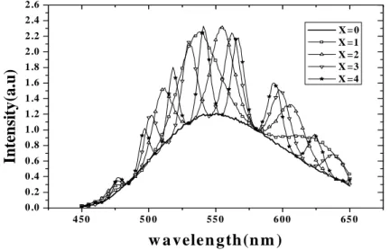
(like some polymers) to serve as the functions of passivation and stress relaxation, respectively. However, due to the limitation of layer numbers in our simulation program, we regard the passivation layers as one single thick layer with an effective refractive index when the thickness of such a layer exceed ten times of the wavelength. With a simplified device structure, we found that the simulation results are quite similar between the case of using a single thick and multiple pair passivation layers with the same optical length. Such results will be published elsewhere. Typically, passivation layer over the top-emission OLED is several micrometers in thickness. Fig. 7 illustrates
Fig. 7 Simulation results of intensity (at viewing angle=0°) as a function of different passivation layer thickness. OLED structure: Ag/ 60nm NPB/ 60nm Alq3/ 20nm Ag/Xμm passivation layer( refractive index=1.45).
0 10 2 0 30 40 50 0 .0 0 .5 1 .0 1 .5 2 .0 2 .5 3 .0 3 .5 4 .0 4 .5 5 .0
In
te
n
sity
(a
.u
)
ca th o d e th ick n ess (n m )
0n m 5n m 10 nm 15 nm 20 nm 25 nm 30 nm 35 nm 40 nm 45 nm 50 nm 55 nm 4 50 5 0 0 55 0 6 00 65 0 0 .0 0 .2 0 .4 0 .6 0 .8 1 .0 1 .2 1 .4 1 .6 1 .8 2 .0 2 .2 2 .4 2 .6In
te
n
si
ty
(a
.u
)
w a v elen g th (n m )
X = 0 X =1 X =2 X =3 X =4the output EL when the passivation layer is about several micrometers. With increasing the dielectric layer thickness, the more peaks appears and the spacing among peaks become closer. The spectrum of such a device exhibits multiple peaks which correspond to the free spectral range of the fabry-perot cavity formed by this layer. It can be described as ∆f=c/2nL where c is the velocity of light in vacuum, n is the refractive index of SiO2, and L is the
thickness of SiO2. The microcavity effect results in the presence of multi-peaks. It limits the view angle and
decreases the color purity. Fig. 7 illustrates EL spectrum when the passivation compound of SiO2 and several
different materials. It shows that when the refractive index difference between the two materials is larger, the amplitude oscillation of the EL spectrum is bigger. This is a serious problem with three pair of this stack structure for passivation layer. It will change the top-emission OLED EL spectrum different when adding the passivation layer.
In order to overcome the oscillation problem, we increase the thickness of the passivation layer. The spacing among peaks become closer and it will become indistinguishable when the thickness is over 10 µm. Figure 8 shows the simulation results of output EL spectrum (at viewing angle =0°) of OLED device with different passivation layer structure. Although the EL spectrum still has some small oscillations, it does not affect the CIE obviously. The device without dielectric and passivation layer has the lowest intensity. Adding a passivation layer on the TOLED device can enhance the efficiency and the EL spectrum does not change obviously. Besides, we can add a dielectric layer between the cathode and the passivation layer to enhance the output coupling efficiency. With simulation results, when the dielectric layer is 35nm, we can obtain the highest output efficiency.
FIG.8. Simulation results of EL spectrum (at viewing angle=0°) with different passivation structure. Device structure: Ag/ 60nm NPB/ 60nm Alq3/ 20nm Ag/ passivation structure. The dielectric layer(refractive index=2.6) is 35nm and the passivation layer(refractive index=1.45) is 10μm.
4. SUMMARY
In this paper, we have shown the simulation results of a TOLED with a passivation layer. Such a layer is typically several micrometers in thickness. The spectrum of such a device exhibits multiple peaks which correspond to the free spectral range of the fabry-perot cavity formed by this layer. The microcavity effect may result in the presence of multi-peaks. It limits the view angle and decreases the color purity. With increasing the thickness of the passivation layer, the spacing among peaks become closer and it will become indistinguishable when the thickness is
450 500 550 600 650 0 1 2 3 4
In
te
n
si
ty
(
a
.u
)
wavelength (nm)
without dielectric and passivation layer w ith dielectric and passivation layer only w ith passivation layer
over 10 µm, and the spectrum does not change much. Besides, we can add a dielectric layer between the cathode and passivation layer to enhance to out coupling efficiency.
REFERENCES
1. C. W. Tang and S. A. Vanslyke, Appl. Phys. Lett. 51, 913 (1987). 2. S. Möller and S. R. Forrest, J. Appl. Phys 91 3324 (2003)
3. H. Riel, S. Karg, T. Beierlein, B. Ruhstaller, and W. Rieβ, Appl. Phys. Lett. 82 466 (2003)
4. Seung Ho Kwon, Sang Yoon Paik, Oh Jun Kwon, and Jae Soo Yoo, Appl. Phys. Lett. 79, 4450 (2001) 5. J. A. E. Wasey and W.L. Barnes, J. Modern Optics. 47, 725 (2000)
6. K. B. Kahen, Appl. Phys. Lett. 78 1649 (2001)
7. J. R. Wait, IEEE Trans. On Antennas and Propagation 15 645 (1967)
8. A. W. Biggs and H. Myron Swarm, IEEE Trans. On Antennas and Propagation 16 201 (1968)
9. A. Ishimaru, “Electromagnetic Wave Propagation, Radiation, and Scattering” London: Prentice-Hall International (1991)