國 立 交 通 大 學
電子工程學系 電子研究所
碩 士 論 文
氧空缺與相變化在氮化鈦/二氧化矽/鐵白金
結構電阻式非揮發性隨機存取記憶體的影響
The Role of Oxygen Vacancies and Phase Change in
TiN/SiO
2/PtFe Resistance nonvolatile Random Access
Memories
研 究 生 : 張 耀 峰
指導教授 : 張 俊 彥 院士
氧空缺與相變化在氮化鈦/二氧化矽/鐵白金結構
電阻式非揮發性隨機存取記憶體的影響
The Role of Oxygen Vacancies and Phase Change in
TiN/SiO
2/PtFe Resistance nonvolatile Random Access
Memories
研 究 生: 張 耀 峰
Student:
Yao-Feng
Chang
指導教授: 張 俊 彥 院士
Advisor:
Dr.
Chun-Yen
Chang
國 立 交 通 大 學
電子工程學系 電子研究所
碩 士 論 文
A thesis
Submitted to Department of Electronics Engineering and
Institute of Electronics
College of Electrical and Computer Engineering
National Chiao Tung University
In Partial Fulfillment of the Requirements
For the Degree of
Master
In
Electronics Engineering
June 2009
Hsinchu, Taiwan, Republic of China
氧空缺與相變化在氮化鈦/二氧化矽/鐵白金結
構電阻式非揮發性隨機存取記憶體的影響
學生:張耀峰 指導教授:張俊彥 教授
國立交通大學電子工程學系電子研究所碩士班
摘要
近年來,由於非揮發性記憶體的應用與發展受到矚目,加上快閃記憶體微縮 極限,所以新世代非揮發性記憶體的研究正緊鑼密鼓地展開。其中,電阻式非揮 發性記憶元件具有高密度、高操作速度、低功率消耗、高耐久性、微縮能力高及 非破壞性資料讀取等優點,使其成為新世代非揮發性記憶元件的熱門人選。 在本篇論文中,提出電阻轉換特性的物理模型與理論基礎在氮化鈦/二氧化 矽/鐵白金的結構上,且與氧空缺和相變化有關。其內容可分為三大部份,包含 利用結構上的不同,亦或不同熱處理的方式與小尺寸元件效應,來驗證論文中所 提到的物理模型與電性特性的研究。在利用不同結構來檢視記憶體特性部份,置 換不同上下電極材料與二氧化矽厚度,來檢視電阻有效轉態區的位置。其結果驗 證有效轉態區位置在鐵白金底電極與二氧化矽的界面上,且和 Fe 元素有一定的 相關性。在利用不同的熱處理方式來檢視電阻轉態特性部分,驗證了氧化鐵與氧 空缺量的多寡程度亦會影響到轉態週期與電流特性。最後,製作小尺寸元件來檢 視轉態特性,發現實驗結果與電性水管理論的結果相似,並且可從電性結果更加 驗證物理模型的確立。最後提出電性水管的基本物理與數學模型,做為未來可能 再增進的研究方向。The Role of Oxygen Vacancies and Phase
Change in TiN/SiO
2/PtFe Resistance nonvolatile
Random Access Memories
Student: Yao-Feng Chang Advisor: Prof. Chun-Yen Chang
Department of Electronics Engineering and Institute of Electronics
National Chiao Tung University
Abstract
Recently, since nonvolatile memories acquire a lot of attention and flash memories are facing with the scale limit issue, the next generation nonvolatile memory has been carried out to discover extensively. The resistive random access memories (ReRAMs) that have the strengths of high cell density array, high operation speed, low power consumption, high endurance, lower scale limit and non-destructive readout, are one of the most potential candidate for flash memories.
In this thesis, a physical model and mechanism which is about the role of oxygen
vacancies and phase change in TiN/SiO2/PtFe resistance nonvolatile random access
memories is proposed. This study can be categorized into three parts, different structures, different thermal treatments and small size devices, all of these electrical results can support the model and mechanism. In the first part, replacing metal
electrode materials and SiO2 thickness with different structures was found the results
plays an important role to cause resistance switching behavior. In the second part, with different thermal treatments to examine the resistance switching characteristics,
was discovered that amount of Fe2O3 and oxygen vacancies would affect endurance
reliability and electric characteristics. In the third part, using small size cells to examine the resistance switching characteristics was found the results which are similar with the electric faucet theory and the proposed model. Moreover, a possible model about electric faucet is proposed by physical and mathematical methods. Further investigation, including interfacial electric faucet structure and electrode effects, would help to achieve a better understanding.
誌謝
Contents
CHINESE ABSTRACT ... I ABSTRACT ... II ACKNOWLEDGEMENT ... IV CONTENTS ... V TABLE CAPTIONS ... IX FIGURE CAPTIONS ... X CHAPTER 1 INTRODUCTION1.1INTRODUCTION TO NON-VOLATILE MEMORY ... 1
1.1.1 Flash ... 2
1.1.2 Resistive random access memory (ReRAM) ... 2
1.1.3 Structure and fabrication ... 3
1.1.4 Material classification ... 4
1.1.5 Operation and circuit realization ... 4
1.2CONDUCTING MECHANISMS IN OXIDES [25] ... 6
1.2.1 Ohmic conduction ... 6
1.2.2 Space charge limited current ... 7
1.2.3 Schottky emission ... 8
1.2.4 Frenkel-Poole emission ... 8
1.2.5 Tunneling ... 9
1.3MODELS OF RESISTIVE SWITCHING MECHANISMS... 9
1.3.1 Filament-type resistive switching [23] ... 10
CHAPTER 2 EXPERIMENT DETAILS ... 16
2.1MOTIVATION ... 16
2.2SAMPLE FABRICATION ... 16
2.2.1 Standard RCA clean ... 17
2.2.2 Growth of buffer SiO2 ... 18
2.2.3 Deposition of bottom electrode ... 18
2.2.4 Preparation of insulator SiO2 ... 19
2.2.5 Deposition of top electrodes ... 19
2.2.6 Deposition of passivation oxide ... 20
2.2.7 Deposition of probing electrodes ... 20
2.3ANALYSES AND MEASUREMENTS ... 20
2.3.1 Inductively coupled plasma-mass spectrometry (ICP-MS) ... 21
2.3.2 X-ray diffraction (XRD) ... 21
2.3.3 X-ray photoelectron spectrometer (XPS) ... 21
2.3.4 Auger electron spectroscopy (AES) ... 21
2.3.5 Secondary ion mass spectroscopy (SIMS) ... 22
2.3.6 Electrical measurements ... 22
2.3.6.1 Bistable resistive switching ... 23
2.3.6.2 Endurance ... 23
2.3.6.3 Retention ... 23
CHAPTER 3 RESULTS AND DISCUSSIONS ... 26
3.1DEVICE STRUCTURES AND CHARACTERISTICS ... 26
3.1.1 Various bottom electrode metals ... 26
3.1.1.1 Mechanism of Forming Process ... 27
3.1.1.3 Mechanism of Oxygen Vacancies in the Reset Process ... 28
3.1.1.4 Band diagram in the Reset Process ... 29
3.1.1.5 Mechanism of Phase Change in the Set Process ... 29
3.1.1.6 Mechanism of Oxygen Vacancies in the Set Process ... 30
3.1.1.7 Band diagram in the Set Process ... 31
3.1.2 Effects of Top Electrode Metal Effects ... 31
3.1.3 Effects of SiO2 Thicknesses ... 32
3.1.4 Summary I ... 32
3.2EFFECTS OF BOTTOM ELECTRODE METALS ... 33
3.2.1 Electrical properties ... 33
3.2.1.1 Bistable Resistance switching ... 33
3.2.1.2 Current-Voltage Fitting ... 34
3.2.1.3 I-V Characteristics Distribution ... 34
3.2.2 Summary II ... 35
3.3THERMAL TREATMENT EFFECTS ... 35
3.3.1 Electrical Characteristics ... 36
3.3.1.1 Bistable resistance switching and Endurance ... 36
3.3.2 Material analysis ... 37 3.3.2.1 SIMS ... 37 3.3.2.2 XPS ... 37 3.3.2.3 XRD ... 38 3.3.3 Comprehensive Comparison ... 38 3.3.3.1 Endurance Reliability ... 38
3.3.3.2 The Low Resistance State ... 39
3.4SMALL SIZE EFFECTS ... 41
3.4.1 Experimental ... 41
3.4.2 Bistable Resistance Switching ... 41
3.4.3 Material Analysis ... 42
3.4.4 Current Fitting ... 42
3.4.5 Size Effects ... 43
3.4.6 Set Process with Different Sizes ... 44
3.4.7 Reset Process with Different Sizes ... 44
3.4.8 Compliance Current and Switching Process ... 45
3.4.8.1 Physical Model of Electric Faucet ... 45
3.4.8.2 Mathematical Model of Electric Faucet ... 47
3.4.9 Summary ... 48
CHAPTER 4 CONCLUSION ... 83
Table Captions
Figure Captions
FIGURE 1-1.TYPICAL LINEAR I-V CURVES OF RRAM SWITCHING IN VOLTAGE SWEEPING MODE
(UNIPOLAR)[23]. ... 11
FIGURE 1-2.TYPICAL LINEAR I-V CURVES OF RRAM SWITCHING IN VOLTAGE SWEEPING MODE.(BIPOLAR) [23] ... 11
FIGURE 1-3.SWITCHING DYNAMICS MONITORED WITH PROGRAMMING AND READING PULSES.PULSE
WAVEFORMS AND TRANSITION FOR (A) SET PROCESS AND (B) RESET PROCESS.[24] ... 12
FIGURE 1-4.CONCEPTUAL SCHEMATIC OF 1D1R STRUCTURE.[24] ... 12
FIGURE 1-5.CROSS-SECTIONAL SCHEMATIC AND BASIC CIRCUIT DIAGRAM OF 1T1R STRUCTURE.[26] .. 13
FIGURE 1-6.(A)GENERALIZED CROSS-POINT STRUCTURE WITH MEMORY AND SWITCHING ELEMENTS.(B)
READING INTERFERENCE WITHOUT SWITCH ELEMENTS.(C)RECTIFIED READING OPERATION WITH
SWITCH ELEMENTS.[27] ... 13
FIGURE 1-7.SCHEMATIC OF THE FILAMENT IN AN OXIDE.[28] ... 14
FIGURE 1-8.CONDUCTIVITY MAPPING RESULTS OF THE (A) LOW RESISTANCE AND (B) HIGH RESISTANCE
STATE TIO2 FILMS, USING CONDUCTIVE AFM(CAFM).THE BRIGHT SPOTS REPRESENT THE
CONDUCTING POINTS.[12] ... 14
FIGURE 1-9.BAND DIAGRAM WITH THE CONDITIONS OF P-TYPE SEMICONDUCTOR FOR ON STATE (LRS)
AND OFF STATE (HRS), RESPECTIVELY.[23] ... 15
FIGURE 2.1.SCHEMATIC DIAGRAM OF TI/TIN/SIO2/PTFE/SIO2/SI STRUCTURE, AND ITS SMALL SIZE
STRUCTURE. ... 24
FIGURE 2.2.PROCESS FLOWS OF TI/TIN/SIO2/PTFE/SIO2/SI STRUCTURE, AND ITS SMALL SIZE STRUCTURE.
... 25
FIGURE 3.1.SCHEMATIC DIAGRAM OF AL/SIO2/PT/SIO2/SI STRUCTURE. ... 50
FIGURE 3.3.PROCESS FLOWS OF TI/TIN/SIO2/PT/SIO2/SI STRUCTURE. ... 51
FIGURE 3.4.INITIAL STATE OF AL/SIO2/PT/SIO2/SI STRUCTURE. ... 51
FIGURE 3.5.I-V CHARACTERISTICS OF AL/SIO2/PT STRUCTURE AFTER FORMING. ... 52
FIGURE 3.6.SCHEMATIC DIAGRAM OF AL/SIO2/PTFE/SIO2/SI STRUCTURE. ... 52
FIGURE 3.7.PROCESS FLOWS OF TI/TIN/SIO2/PTFE/SIO2/SI STRUCTURE. ... 53
FIGURE 3.8.I-V CHARACTERISTICS OF TI/TIN/SIO2/PTFE STRUCTURE DURING SET AND RESET PROCESSES. ... 53
FIGURE 3.9.I–V CHARACTERISTICS DURING THE FORMING PROCESS IN THE AL/SIO2/PT STRUCTURE. .... 54
FIGURE 3.10.IMPACT IONIZATION BREAKDOWN IN THE AL/SIO2/PT STRUCTURE. ... 54
FIGURE 3.11.AFTER FORMING PROCESS IN AL/SIO2/PT/SIO2/SI STRUCTURE.THERE IS SOME LOW RESISTANCE PATHS PRODUCED IN SIO2 INSULATING FILM. ... 55
FIGURE 3.12.INITIAL STATE OF AL/SIO2/PTFE STRUCTURE. ... 55
FIGURE 3.13.I–V CHARACTERISTICS DURING THE FORMING PROCESS IN THE AL/SIO2/PTFE STRUCTURE. ... 56
FIGURE 3.14.IMPACT IONIZATION BREAKDOWN IN AL/SIO2/PTFE STRUCTURE. ... 56
FIGURE 3.15.AFTER FORMING PROCESS FOR AL/SIO2/PTFE STRUCTURE, THERE IS SOME LOW RESISTANCE PATHS PRODUCED IN SIO2 AND FE2O3 INSULATING FILM. ... 57
FIGURE 3.16.DURING RESET PROCESS FOR AL/SIO2/PTFE STRUCTURE, THE OXYGEN ION WOULD BE ATTRACTED TO THE BOTTOM ELECTRODE BECAUSE OF THE ELECTRICAL FIELD. ... 57
FIGURE 3.17.DURING RESET PROCESS FOR AL/SIO2/PTFE STRUCTURE, THE LOCALIZATION JOULE HEATING UP TO 1000K WOULD LET FE2O3 FORM. ... 58
FIGURE 3.18.AFTER RESET PROCESS FOR AL/SIO2/PTFE STRUCTURE, THE FE3O4 WOULD CHANGE PHASE TO FE2O3. ... 58
FIGURE 3.19.BAND DIAGRAM OF HIGH RESISTANCE STATE FOR LIGHTED N-TYPE FE2O3 SEMICONDUCTOR. ... 59
THE HIGH BIAS REGION AT HRS(SECTION 3.4.4). ... 59
FIGURE 3.21.DURING SET OR FORMING PROCESS FOR AL/SIO2/PTFE STRUCTURE, THE OXYGEN ION WOULD BE REPELLED TO THE BOTTOM ELECTRODE BECAUSE OF THE ELECTRICAL FIELD. ... 60
FIGURE 3.22.AFTER SET OR FORMING PROCESS FOR AL/SIO2/PTFE STRUCTURE, THE FE2O3 WOULD CHANGE PHASE TO FE3O4 AT SOME ELECTRIC FAUCET REGIONS. ... 60
FIGURE 3.23.BAND DIAGRAM OF LOW RESISTANCE STATE FOR ENHANCED N-TYPE FE2O3 SEMICONDUCTOR. ... 61
FIGURE 3.24.FOR TI/TIN/SIO2/PTFE STRUCTURE, THE RELATIONSHIP BETWEEN TUNNELING CURRENT AND DIFFERENT TEMPERATURE AT LRS(SECTION 3.4.4). ... 61
FIGURE 3.25(A).I-V CURVE OF AL/SIO2/PTFE STRUCTURE. ... 62
FIGURE 3.25(B).I-V CURVE OF TI/TIN/SIO2/PTFE STRUCTURE. ... 62
FIGURE 3.25(C).I-V CURVE OF W PROBE/SIO2/PTFE STRUCTURE. ... 63
FIGURE 3.26(A).SCHEMATIC DIAGRAM OF TI/TIN/SIO2(50NM)/PTFE STRUCTURE. ... 63
FIGURE 3.26(B).SCHEMATIC DIAGRAM OF TI/TIN/SIO2(30NM)/PTFE STRUCTURE. ... 63
FIGURE 3.27(A).I-V CURVE OF TI/TIN/SIO2(50NM)/PTFE/SIO2/SI STRUCTURE. ... 64
FIGURE 3.27(B).I-V CURVE OF TI/TIN/SIO2(30NM)/PTFE/SIO2/SI STRUCTURE. ... 64
FIGURE 3.28(A).SCHEMATIC DIAGRAM OF TI/TIN/SIO2/PTFE STRUCTURE. ... 65
FIGURE 3.28(B).SCHEMATIC DIAGRAM OF TI/TIN/SIO2/FE/PT/TI STRUCTURE. ... 65
FIGURE 3.28(C).PROCESS FLOWS OF TI/TIN/SIO2/PTFE AND TI/TIN/SIO2/FE/PT/TI STRUCTURES. ... 65
FIGURE 3.29(A).I-V CURVE OF TI/TIN/SIO2/PTFE STRUCTURE. ... 66
FIGURE 3.29(B).I-V CURVE OF TI/TIN/SIO2/FE/PT/TI STRUCTURE. ... 66
FIGURE 3.30.FOR PTFE AND FE BOTTOM ELECTRODE STRUCTURE, CURRENT FITTING RESULTS OF LRS (UPPER LEFT), SMALL BIAS REGION AT HRS(LOWER LEFT), AND HIGH BIAS REGION AT HRS(LOWER RIGHT). ... 67
FIGURE 3.31(B).STATISTICS PLOT OF THE RELATIONSHIP BETWEEN SET (RESET) CURRENT AND DIFFERENT
BOTTOM ELECTRODE STRUCTURES. ... 68
FIGURE 3.31(C).STATISTICS PLOT OF THE RELATIONSHIP BETWEEN SET (RESET) POWER AND DIFFERENT
BOTTOM ELECTRODE STRUCTURES. ... 68
FIGURE 3.32(A).I-V CURVE OF TI/TIN/SIO2/PTFE STRUCTURE (AS DEPOSITION). ... 69
FIGURE 3.32(B).ENDURANCE OF THE TI/TIN/SIO2/PTFE STRUCTURE ABOUT 300 TIMES (AS DEPOSITION).
... 69
FIGURE 3.33(A).I-V CURVE OF TI/TIN/SIO2/PTFE STRUCTURE (FURNACE ANNEALING 600
O
C,30MIN IN
VACUUM). ... 70
FIGURE 3.33(B).ENDURANCE OF THE TI/TIN/SIO2/PTFE STRUCTURE OVER 1000 TIMES (FURNACE
ANNEALING 600O
C,30MIN IN VACUUM). ... 70
FIGURE 3.34(A).I-V CURVE OF TI/TIN/SIO2/PTFE STRUCTURE (RAPID THERMAL ANNEALING 600
O
C60S,
ATMOSPHERIC PRESSURE IN N2 OR AIR CONDITION). ... 71
FIGURE 3.34(B).ENDURANCE OF THE TI/TIN/SIO2/PTFE STRUCTURE OVER 1000 TIMES (RAPID THERMAL
ANNEALING 600O
C60S, ATMOSPHERIC PRESSURE IN N2 OR AIR CONDITION). ... 71
FIGURE 3.35.STATISTICS PLOT OF THE RELATIONSHIP BETWEEN HRS(LRS) READING CURRENT AT 0.2V
AND DIFFERENT THERMAL TREATMENT CONDITIONS. ... 72
FIGURE 3.36.SIMS RESULTS OF TI/TIN/SIO2/PTFE STRUCTURE DURING RTA OR FA THERMAL
TREATMENT. ... 72
FIGURE 3.37.XPS RESULTS OF SIO2 AND PTFE INTERFACE REGION (AS-DEPOSITION,FA AND RTA
THERMAL CONDITION). ... 73
FIGURE 3.38.XRD RESULTS OF AS-DEPOSITED,FA AND RTA SAMPLE. ... 73
FIGURE 3.39.THE POSSIBLE MECHANISMS FOR FA AND RTA SAMPLE AFTER FORMING OR SET PROCESS. 74
FIGURE 3.40.STATISTICS PLOT OF THE RELATIONSHIP BETWEEN SET VOLTAGE AND DIFFERENT THERMAL
FIGURE 3.41(B).PROCESS FLOWS OF SMALL SIZE TI/TIN/SIO2/PTFE/SIO2/SI STRUCTURE. ... 75
FIGURE 3.41(C).I-V CURVE OF TI/TIN/SIO2/PTFE STRUCTURE (TOP ELECTRODE AREA:7.5UM2). ... 76
FIGURE 3.42(A).AES RESULTS OF SMALL SIZE TI/TIN/SIO2/PTFE STRUCTURE. ... 76
FIGURE 3.42(B).XPS RESULT BETWEEN SIO2 AND PTFE BOTTOM ELECTRODE INTERFACE REGION. ... 77
FIGURE 3.43.FOR SMALL SIZE STRUCTURE, CURRENT FITTING RESULTS OF LRS(UPPER LEFT, INSERT SHOWS LESS TEMPERATURE SENSITIVITY), SMALL BIAS REGION AT HRS(LOWER LEFT), AND HIGH BIAS REGION AT HRS(LOWER RIGHT)(INSERT SHOWS FP EMISSION MODE AT DIFFERENCE TEMPERATURE). ... 77
FIGURE 3.44.STATISTICS PLOT OF THE RELATIONSHIP BETWEEN HRS(LRS) RESISTANCE AND DEVICE SIZE. ... 78
FIGURE 3.45(A).STATISTICS PLOT OF THE RELATIONSHIP BETWEEN SET CURRENT DENSITY AND DEVICE SIZE. ... 78
FIGURE 3.45(B).STATISTICS PLOT OF THE RELATIONSHIP BETWEEN SET VOLTAGE AND DEVICE SIZE. ... 79
FIGURE 3.45(C).STATISTICS PLOT OF THE RELATIONSHIP BETWEEN SET POWER PER AREA AND DEVICE SIZE. ... 79
FIGURE 3.46(A).STATISTICS PLOT OF THE RELATIONSHIP BETWEEN RESET CURRENT AND DEVICE SIZE. . 80
FIGURE 3.46(B).STATISTICS PLOT OF THE RELATIONSHIP BETWEEN RESET VOLTAGE AND DEVICE SIZE. .. 80
FIGURE 3.46(C).STATISTICS PLOT OF THE RELATIONSHIP BETWEEN RESET POWER AND DEVICE SIZE. ... 81
FIGURE 3.47.STATISTICS PLOT OF THE RELATIONSHIP BETWEEN 0.5V READ RESISTANCE AND COMPLIANCE CURRENT. ... 81
FIGURE 3.48.RELATIONSHIP BETWEEN ELECTRIC FAUCET’S CROSS SECTION AREA AND COMPLIANCE CURRENT. ... 82
FIGURE 3.49.STATISTICS PLOT OF THE RELATIONSHIP BETWEEN RESET POWER AND COMPLIANCE CURRENT. ... 82
Chapter 1
Introduction
1.1 Introduction to non-volatile memory
Recently, the portable electronic products possess wide applications. These products are all based on flash memory which is considered as a technology drivers for semiconductor industry in the next generation. It can be classified into two major markets: code storage application and data storage application. NOR type flash
memory [1] has been targeted at code storage application, such as PC bios and DVD
player. NAND type flash memory [2] is the most suitable for code storage application,
such as PDA, memory cards, MP3 audio players, digital cameras, and USB flash personal disc etc. These products are all based on flash memory that is nonvolatile and can keep stored information when the power supply is switched off. The first NVM is the floating-gate nonvolatile memory, invented by S. M. Sze and D. Kahng at Bell
Labs in 1967 [3]. A perfect NVM should possess the properties including low
operation voltage, simple structure, low power consumption, non-destructive readout,
high operation speed, long retention time, high endurance, and small cell size [4, 5].
There have been many kinds of nonvolatile memories invented so far, such as flash memory, erasable programmable read only memory (EPROM), electrically erasable programmable read only memory (EEPROM), phase change memory (PCRAM), ferroelectric random access memory (FeRAM), magnetoresistive random access memory (MRAM), and resistance random access memory (RRAM). Today, flash memory is the mainstream among the NVMs.
The following will concentrate on the next generation nonvolatile memory, ReRAM. Flash memories are also introduced.
1.1.1 Flash
Flash memory, invented by Gerard Dixon, is a form of nonvolatile computer memory, which can be electrically erased and reprogrammed.
Flash memory stores information in an array of floating gate transistors, called “cells”, each of cells stores one bit of information. The latest flash memory devices, often referred to as multi-level cell devices, could store more than 1 bit per cell, by using more than two levels of electrical charge which is placed on the floating gate of a cell. The writing times for common flash memory devices are in the order of 1 ms, and reading times are typical 10 ns.
When manufacturers increase the density of flash devices, each cells shrink and the number of electrons in any cells become few. Coupling effect between adjacent floating gates could change the cell characteristics. New designs, like charge trap flash, try to provide better isolation between adjacent cells.
Although the flash memory is the mainstream device of NVM, flash memory possesses the defects including high operation voltage, low operation speed, and low endurance. Moreover, following the device scaling, tunneling oxide would be shrunken, which would lead to a large leakage current due to tunneling current. Hence, because of device scaling, the retention time of flash memory would be reduced.
1.1.2 Resistive random access memory (ReRAM)
generation nonvolatile memory devices. RRAMs use of the resistance changes as different memory states. By electrical field or current effects, the conductivity could be switched between high and low resistance reproducibly. The bistable resistance states represent different digital states as a memory device. The advantages of RRAM are the high cell density array, high operation speed, low power consumption, high endurance and lower scale limit. Moreover, RRAMs possess the features of nonvolatility, long retention time, and non-destructive readout. In next section, the properties of structure, fabrication, material classification, operation and circuit realization will be discussed.
1.1.3 Structure and fabrication
The basic structure for RRAM is made up of only metal-insulator-metal, M-I-M, which could be further integrated into 1D1R (a diode and a resistor) or 1T1R (a
transistor and a resistor) structures (discussed later) [6, 7]. The top and bottom
electrodes could be made by metals or conducting transition metal oxides [6], the
choice of which would impact on the resistive switching properties because of their different crystallinities, work functions and the ability of oxygen gettering [8-10].
The main character of resistive switching is the insulator layer sandwiched among the electrodes. The insulator for the M-I-M structure may be not really insulating, but also semiconducting, depending on the composition and stoichiometry
[11]. The insulator would be called “resistance switching layer” in the following
sections. The different qualities deposited by different methods would possess connection with the resistive switching characteristics [12].
1.1.4 Material classification
The resistive switching phenomena have been discovered in many materials. The research mainstream concentrates on several groups, including binary oxides, perovskite oxides, manganites, and organic or polymers.
The binary oxides adopted in RRAM application, such as TiO2[13], ZrO2 [14],
NiO [15], Al2O3[16], CuxO [17], Fe2O3[18], ZnO [19], HfO2[10], SiO2[20, 21] and
MoOx[22], are candidates or have been widely used in other field of CMOS devices.
Thus, the compatibility with modern CMOS process would not be a serious issue. Moreover, these binary oxides possess simpler element and it could be easier to control the proportion metal and oxygen composition.
1.1.5 Operation and circuit realization
Basic operation of bistable resistive switching in one cell could be achieved by
DC sweep or pulse modes. Fig. 1-1 and Fig. 1-2 show a typical I-V plot under DC
sweep operation, unipolar and bipolar mode [23]. First, assuming the resistance state
is held in high resistance state, the current would suddenly increase when DC bias sweeps toward the same (or opposite) direction. Hence, the resistance would become low resistance state, which is defined as a process of “set”. Then the opposite (or same) direction bias is applied to switch back to high resistance state with an enormously current drop at the switching voltage, which is defined as a process of “reset”. It should be noted that this operation requiring different (or same) voltage polarities to switch, whether negative on/positive off or negative off/positive on (or positive on/positive off or negative off/negative on), is called bipolar operation (unipolar operation). For reading operation, the bias should not exceed the switching voltage (set or reset) to prevent memory state variation. Fig. 1-1 and Fig. 1-2 do not show the
forming process which is required to initiate the resistive switching properties of oxide films. The forming process is similar to soft breakdown, leading to the conducting paths (filaments) composed of clusters of point defects. In order to unify the operation parameters in the following text, the “set” and “reset” would be used to describe the switching operation; “Vset”, “Vreset”, “RLRS” and “RHRS” would be used to
describe the set voltage, reset voltage, the resistance at low resistance state (LRS) and the resistance at high resistance state (HRS).
In the real circuits, it is the pulse mode of switching that is the practical operation method due to fast operation speed and lower power consumption. The waveforms of set and reset process are shown in Fig. 1-3(a) and (b) respectively. The pulse heights
and widths for set and reset must take a balance. The larger of pulse heights are, the shorter of the pulse widths are needed. The reading pulses with small pulse heights are also designed not to vary the memory states.
For the memory array structure, 1D1R (1 diode and 1 resistor) or 1T1R (1
transistor and 1 resistor) structure (Fig. 1-4 and Fig. 1-5) must be used to prevent
misreading as shown in Fig. 1-6. I. G. Baek et al. [24] reported that if a cell is in high
resistance state and its neighboring cells are in low resistance state, it will be misread as low resistance state due to the leakage current path around its neighboring cells. Hence, a rectifying element is required for each cell in an array to limit the current
paths. The minimum sizes for 1D1R and 1T1R structures are 4F2 and 6F2 respectively,
1.2 Conducting mechanisms in oxides
[25]
Based on conductivity, transition metal oxides could be insulator, semiconductor or metal depending on the composition of the oxide materials. Hence the conducting mechanisms may vary because of their different physics and chemistry characteristics. The widely discussed materials in RRAM application generally belong to insulator or semiconductor according to the constitution and stoichiometry, and the electron conduction mechanisms mostly involved are Ohmic conduction, space charge limited current, Schottky emission, Frenkel-Poole emission and Tunneling. Furthermore, the current fitting procedure would give insight into the conduction mechanisms.
1.2.1 Ohmic conduction
Ohmic conduction takes place when the injected carrier density is far less than the thermally-generated carrier density. Generally, it applies to the condition of low electric field region in which thermally-generated carriers are dominant in conduction. The current-voltage characteristics follow Ohm’s law that the current passing through a resistor from one terminal to the other is proportional to the voltage drop across two points. In addition, the temperature effect is also described in Ohmic conduction behavior. Due to the electron and phonon scattering effects, the conductivity rises with increasing temperature for conduction in semiconductor, while with decreasing temperature for metal conduction. The following is the expression for Ohmic conduction: J aVexp -c T ⎛ ⎞ = ⎜ ⎟ ⎝ ⎠
1.2.2 Space charge limited current
The mechanism of space charge limited current (SCLC) is attributed to defects and usually exists in the dielectric stress by high electric fields. After charge injection from an electrode, the space charge may form if the charge carriers are trapped and distributed over a region of area without being neutralized. The further flow of charge carriers would be impeded by this space charge region. It should be noted that the injected carriers are most electrons. As for conductive media, the trapped carriers can be neutralized or screened rapidly; therefore, the space charge region would not form.
The completely trapped and controlled SCLC mechanism is composed into two
stages [24], trap-unfilled SCLC and trap-filled SCLC, both can be written as the
following expression: 2 0 3 9 1 8 r V J L θ ε ε μ θ ⎛ ⎞ = ⎜⎝ + ⎟⎠
J is the current density, θ is the ratio of free electron to trapped electron, NC is the
effective density of states in the conductive band, Nt is the number of emptied electron traps, ε0 is the permittivity of free space, εr is the static dielectric constant, μ
is the electron mobility, V is the applied voltage and L is the film thickness. At first stage, the traps that are not filled with charges and the formula can be rewritten with θ <<1 as the following: 2 0 3 9 8 r V J L θ ε ε μ =
As the voltage increases, the majority of traps are occupied by the injected carriers, and the current-voltage characteristics can be again rewritten with θ >>1:
2 0 3 9 8 r V J L ε ε μ =
1.2.3 Schottky emission
Schottky emission is mainly attributed to the Schottky contact of the metal-insulator interface. For the carriers to transport, they must jump across the barrier height of one of the interfaces, travel through the dielectric film, and eventually reach the other side. It is the thermionic emission that enables the carriers (most electrons) to overcome the interface barrier height. Therefore, temperature is the key factor that energetic carriers (hot carriers) are easier to jump across the barrier. The formula of Schottky emission is expressed as below:
2exp - ( -q b qV / 4 r 0d J A T kT φ πε ε ∗ ⎛ ⎞ = ⎜⎜ ⎟⎟ ⎝ ⎠
where A* denotes Richardson constant, Φb is the Schottky barrier height, ε0 is the
permittivity of free space, εr is the dynamic dielectric constant, V is the external
applied voltage and d is the insulator thickness.
1.2.4 Frenkel-Poole emission
Frenkel-Poole emission is pretty much similar to Schottky emission mechanism. The main differences are that Frenkel-Poole emission describes the process for carriers to overcome the barriers resulted from the defect states in the dielectric material, and the barrier lowering is twice as large as that in Schottky emission mechanism. Temperature is also crucial for this carrier transportation process, while electric field plays a more important role in this mechanism than in Schottky emission, which suggests that field effects possess greater impact on defect-related behavior. The current-voltage relationship can be written as the following formula:
exp - ( -q t qV / 4 r 0d J BV kT φ πε ε ⎛ ⎞ = ⎜⎜ ⎟⎟ ⎝ ⎠
where B is a material-related constant, Φt is the trap level, and other parameters are
the same as those in Schottky emission.
1.2.5 Tunneling
Tunneling is the most common conduction mechanism through insulators under high fields. The tunnel emission is a result of quantum mechanism by which the electron wave function can penetrate through a potential barrier. It has the strongest dependence on applied voltage, but it is essentially independent of the temperature. Tunneling mechanism can be divided into direct tunneling and Fowler-Nordheim tunneling where carrier tunnel goes through a partial width of the barrier. The current-voltage relationship can be written as the following formula:
) V b -exp( V 3q ) (q 2m 4 -exp J 2 i 2 3 B * 2 i ∝ ⎥ ⎥ ⎦ ⎤ ⎢ ⎢ ⎣ ⎡ ∝ ξ φ ξ h
where ξ is the electric field in insulator, mi * is the effective mass, φ is the barrier B height, and V is the applied voltage.
1.3 Models of resistive switching mechanisms
The major possible models having been proposed by other research groups are sorted partially as two parts, one is filament-type resistance switching and another is
interface-type resistance switching [23]. The two models may be applied for some
combinations of electrodes and oxide materials. For these models, however, are derived by indirect observation or electrical measurements, but the switching mechanisms are still well know because of the lack of directly proved evidence.
1.3.1 Filament-type resistive switching
[23]
The filament-type model comes from the nature of oxide breakdown and integrity that defects existing in an oxide bulk, such as the interstitials, oxygen
vacancies and metals constitute the leakage current path, indicated in Fig. 1-7 [28].
This model has been proposed since 1970’s and is one of the earliest models in
resistive switching mechanism [29, 30]. Recently, since nonvolatile memories possess
obtained a lot of attention, the further and more detailed studies have been realized to investigate the possible mechanisms. All these proposed models, it is the
filament-type model that prevails in many binary oxide films, such as TiO2[31], ZrO2
[11], NiO [24] and CuxO [17]. The most obvious evidences for the filament-type
model are conductive atomic force microscopy (CAFM) mapping results at low resistance state. C-AFM is one of the power tools to study the local conductivity throughout the film. B. J. Choi et. al. and reported that by scanning the film surface with CAFM, only several conductive points exist and account for the current conduction, as shown in Fig. 1-8[12].
1.3.2 Interface-type resistance switching
[23]
The interface-type resistance switching model is wide-spreading especially in the
material system of PCMO [32] and Nb;STO [33]. This model can be further classified
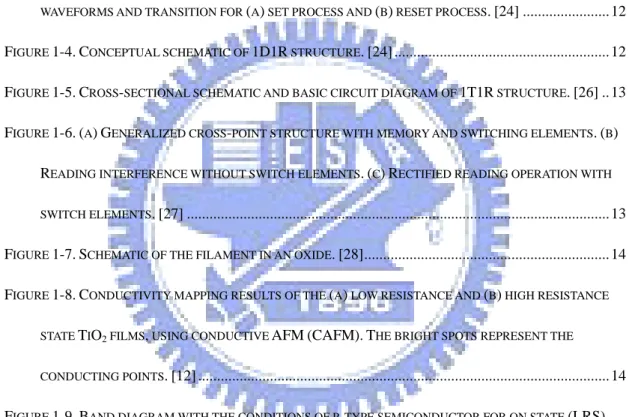
into two types in accordance with the type of semiconductor, the n-type semiconductor and p-type semiconductor. For example, the schematic for p-type semiconductor is illustrated in Fig. 1-9[23].
Figure 1-1. Typical linear I-V curves of RRAM switching in voltage sweeping mode (unipolar) [23].
Figure 1-2. Typical linear I-V curves of RRAM switching in voltage sweeping mode. (bipolar) [23]
Figure 1-3. Switching dynamics monitored with programming and reading pulses. Pulse waveforms and transition for (a) set process and (b) reset process. [24]
Figure 1-5. Cross-sectional schematic and basic circuit diagram of 1T1R structure.
[26]
Figure 1-6. (a) Generalized cross-point structure with memory and switching elements. (b) Reading interference without switch elements. (c) Rectified reading
Figure 1-7. Schematic of the filament in an oxide. [28]
Figure 1-8. Conductivity mapping results of the (a) low resistance and (b) high
resistance state TiO2 films, using conductive AFM (CAFM). The bright spots
Figure 1-9. Band diagram with the conditions of p-type semiconductor for on state (LRS) and off state (HRS), respectively. [23]
Chapter 2
Experiment details
2.1 Motivation
The binary oxides adopted in RRAM application, such as TiO2[13], ZrO2 [14],
NiO [15], Al2O3[16], CuxO [17], Fe2O3[18], ZnO [19], HfO2[10], SiO2[20, 21] and
MoOx[22], are candidates or have been widely used in other field of CMOS devices.
However, few researchers study SiO2 which is a common and compatible material for
CMOS process [20, 21]. Even through several models for the phenomenological
results have been suggested [28], the universal physical origins of the resistance
switching properties are still in question. Hence, in this thesis, SiO2 with different
metal electrode materials and structures, different thermal treatments, and small size structures are studied, and try to find out a possible model and resistance switching mechanism to explain.
2.2 Sample fabrication
In this thesis, the basic structure for studying SiO2 resistance switching behaviors
is depicted in Fig. 2.1. It was fabricated on P-type (100) silicon substrates (20-100
Ω-cm). After a standard RCA cleaning, a 500 nm SiO2 film was grown as a buffer
oxide by LPCVD. Subsequently, 50-nm-thick Fe0.73Pt0.27 layers were deposited by DC
magnetron reactive sputtering method. The PtFe alloy electrode was Co-sputtered with Fe and Pt targets and its composition was measured by Inductively Coupled
Plasma Mass Spectroscopy (ICP-MS). 50nm SiO2 layers were deposited by plasma
enhanced chemical vapor deposition (PECVD) on Fe0.73Pt0.27 electrode at 300oC
ambient. Finally, TiN top electrodes with defining area were formed on the SiO2 films
by DC magnetron reactive sputtering. And then 200nm passivation oxide was
deposited to prevent humid environment. The process flow is depicted in Fig. 2.2, and
all the details in each process are stated below.
2.2.1 Standard RCA clean
The bare Si wafers must be cleaned before further processes. The RCA clean is the industry standard for removing contaminants from wafers, and the main steps are narrated as the following. The wafers were submerged in Caro’s acid (also called
SPM), a solution of 3:1 H2SO4:H2O2, for 10 minutes at around 80oC to remove
organic contaminants from the surface of wafer. Then, the wafers were in 1:100 HF:
H2O (diluted HF, DHF) to etch chemical oxide produced in the previous step. The
following steps were standard clean 1 (SC1) and standard clean 2 (SC2), in which the
wafers were soaked in a solution with 1:4:20 NH4OH:H2O2:H2O and 1: 1:6 HCl:
H2O2: H2O, respectively, both for 10 minutes at around 80oC to eliminate particles and
metallic contamination. Finally, the wafers were dipped in DHF again to remove the chemical oxide grown in the previous standard clean steps. It should be noted that each step was separated by DI water rinse for 5 minutes.
The mechanism for Caro’s acid to remove organic contaminants comes from its strong capability of dehydrating and oxidizing organic compound containing C-H
bonding. As for SC1, the surface of Si wafer is oxidized by H2O2 into a thin SiO2
layer, the footing layer for particles and in the meantime etched by NH4OH. The
finally vanishes. The following SC2 step further takes IA and IIA metal ions away, in
which chlorides resulting from the combination of IA, IIA and Cl- would dissolve in
water and thus the metal ions are eliminated. On the other hand, IIIA metal ions such
as Al would be reactive with NH4OH in SC1 and generates AlOH3 which later forms
chlorides in SC2. Hence, to remove particles and metal ions effectively, the sequential order of SC1 and SC2 cannot be reversed.
2.2.2 Growth of buffer SiO
2After RCA clean, 6-in-boron-doped Si wafers were sent into a furnace
immediately for thermal oxidation, in which SiO2 was grown at 980oC in O2 and H2
atmosphere. The SiO2 layer that plays a role of insulating layer avoiding current
leakage from the Si substrate was expected to be 500 nm in thickness.
According to different mechanisms, there are two types of thermal oxidation, dry
and wet oxidation. The former is oxidized in O2 ambient, in which oxygen ions are
combined with Si atoms to form SiO2. The diffusion barrier for oxygen ions moving
through the existed SiO2 toward Si is getting larger as SiO2 is becoming thicker, and
thus dry oxidation is not suitable for the growth of thick SiO2. For the 500-nm SiO2
required in this study wet oxidation was adopted, using O2/H2 and forming OH- ions
which possess higher mobility going through SiO2, to obtain higher growth speed.
2.2.3 Deposition of bottom electrode
50-nm-thick Fe0.73Pt0.27 layers were deposited by DC magnetron reactive
sputtering method. The PtFe alloy electrode was Co-sputtered with Fe and Pt targets and its composition was measured by Inductively Coupled Plasma Mass Spectroscopy (ICP-MS). We also fabricated two different type electrodes in the bottom to
examination the resistance switching characteristics which would discuss in next section. 50-nm-thick Pt and 5-nm-thick Fe / 80-nm-thick Pt / 20-nm-thick Ti layers were also deposited by DC magnetron reactive sputtering method.
Sputter systems are widely adopted in film deposition due to the simple equipment structure, low cost and the capability of depositing all kinds of films. They use the ions in the plasma to bombard the target, and sputter out a large amount of target species onto the wafer, achieving the purpose of film deposition.
2.2.4 Preparation of insulator SiO
250-nm-thick or 30-nm-thick oxide is deposited by plasma enhanced chemical
vapor deposition (PECVD) system at 300°C. The SiO2 film is an insulator film, and
studies the resistance switching characteristics on (beneath) different metal electrode materials.
2.2.5 Deposition of top electrodes
After deposition of insulator SiO2, the top electrodes are prepared to form the
structure of metal/insulator/metal. In the part of different structures to survey the resistance switching behaviors, the electrodes of 400-nm-thick aluminum (Al) or 80-nm-thick titanium (Ti) / 30-nm-thick titanium nitride (TiN) are deposited by the same DC magnetron reactive sputter system in 24 sccm Ar ambient (TiN electrode is
in 24 sccm Ar + 5 sccm N2). Furthermore, the tungsten (W) probe also can be our top
electrode with the utmost care that the tip does not scratch or perforate the oxide surface.
by lithography and etching having the square-shaped patterns with side of 100 μm, i.e.
areas of 1x10⁻⁴ cm2. Furthermore, the W probe was the dot-shaped needle which
diameter was 5 μm, i.e. areas of 19.63 μm2. Moreover, different small size electrodes
(30-nm-thick TiN) were also patterned by lithography and etching having the rectangle-shaped patterns with side matrix of 0.3, 0.6, 1.5, 3.0 and 5.0 μm.
2.2.6 Deposition of passivation oxide
In order to probe the pattern for small size electrode and prevent humid environment, deposition of the passivation oxide was needed. After the lithography and etching process for small size electrode structure, 200-nm-thickness passivation oxide was deposited by PECVD at 300°C. Then, the lithography and etching process were again needed to etch contact via for probing electrode (contact via is smaller than the top electrode) and bottom electrode (contact hole was square-shaped pattern with side of 100 μm).
2.2.7 Deposition of probing electrodes
After the contact via and contact hole were finished, the probing electrodes (Ti) for small size structure were deposition by DC magnetron reactive sputter system. Deposition of 800-nm-thick Ti on top electrode was patterned by lithography and etching process having the rectangle-shaped patterns with 100 μm side.
2.3 Analyses and measurements
In this thesis, several material analyses and electrical measurements were carried out to study the relationship between material properties and electrical characteristics.
The details will be stated in the following paragraphs.
2.3.1 Inductively coupled plasma-mass spectrometry (ICP-MS)
In order to know PtFe electrode composition, inductively coupled plasma-mass spectrometry is a useful tool to analyze. ICP-MS (Inductively coupled plasma mass spectrometry) is a type of mass spectrometry. It is highly sensitive and can determine
a range of metals and several non-metals at concentrations below 1012. Its mechanism
bases on coupling together inductively coupled plasma, which produces ions (ionization), and a mass spectrometer will separate and detect the ions.
2.3.2 X-ray diffraction (XRD)
X-ray crystallography is the science that can determine the arrangement of atoms within a crystal. The mechanism of X-ray diffraction (XRD) is a beam of X-rays that are scattered from the electrons within the crystal. The most important step in X-ray crystallography is the diffraction of X-rays from a crystalline material.
2.3.3 X-ray photoelectron spectrometer (XPS)
X-ray photoelectron spectroscopy (XPS or someone called Electron spectroscopy of chemical analysis, ESCA) is a quantitative spectroscopic technique and a power tool that can measure the elemental composition, chemical state and electronic state of the elements that exist within a material. XPS spectra are obtained by X-rays shoot on thin films while simultaneously detecting the kinetic energy (KE) and a number of electrons that escape from the top 1 to 10 nm depth of the material.
2.3.4 Auger electron spectroscopy (AES)
study of surfaces. Basically, the spectroscopic technique is the Auger effect. This analyzed technique is based on the analysis of energetic electrons emitted from an excited atom after a series of internal relaxation events. AES is a practical and straightforward characterization technique for probing chemical and compositional of surface.
2.3.5 Secondary ion mass spectroscopy (SIMS)
Secondary ion mass spectrometry (SIMS) is the mass spectrometry of ionized particles which are emitted from a surface that is bombarded by energetic primary particles, such as electrons, ions, neutrals or photons. The emitted secondary particles will be electrons, neutral species atoms, molecules, atomic or cluster ions. The emitted species are neutral but are the secondary ions, which will be detected and analyzed by a mass spectrometer. It can provide a mass spectrum of a surface composition and enable a detailed chemical analysis of a surface. Furthermore, SIMS can also provide a concentration profile of depth because Ar ions can bombard the surface and etch down.
2.3.6 Electrical measurements
The electrical properties were measured by the apparatuses consisting of a probe station with temperature controller, Keithley 4200 semiconductor characterization analyzer and low leakage switch, controlled by a Keithley 4200 computer.
The electrical measurements in this thesis are divided into 2 items, in which bistable resistive switching and endurance for memory device application. Both items will be studied for the fundamental resistive switching mechanisms.
2.3.6.1 Bistable resistive switching
This measurement was performed by Keithley 4200, detecting the conducting current while applying and dual sweeping DC biases on the devices. From the I-V curve, the low resistance state (LRS) has low resistance and high conductivity property, and the high resistance state (HRS) possesses high resistance and low conductivity feature, respectively.
2.3.6.2 Endurance
Endurance is a key feature about memory devices. After enormous number of switching cycles, the memory devices must meet the operation requirements in many applications, such as random access memory (RAM) and solid state disk (SSD). Because these applications need many data write-in operation without any failures, endurance is a basic requirement in almost every type of memory devices. The tests of endurance were carried out by DC biases, and the DC biases were applied to switch devices between LRS and HRS at room temperature (RT).
2.3.6.3 Retention
Retention is also a key feature about nonvolatile memory devices. It stands for the capability of retaining memory data for a long period without any data loss. For a commercially available nonvolatile memory product, the performance of retention is requested to keep ten years. The retention tests were carried out by DC biases which would switch devices to LRS or HRS at RT. Then, the data states were read out at RT once in a given period by applying a 0.2 V (or 0.5V) reading bias and the reading bias must be small enough in order not to vary the existed memory states.
•PtFe (50 nm)
•SiO
2
(500 nm)
•P-Si (100)
•TiN •TiN •TiN •TiN
•TiN
•TiN
•
•
SiO
SiO
2
2
(50nm)
(50nm)
•Ti
•Ti
•Ti
•Ti
•Ti •Ti
•PtFe (50 nm)
•SiO
2
(500 nm)
•P-Si (100)
•TiN •TiN •TiN •TiN
•TiN
•TiN
•
•
SiO
SiO
2
2
(50nm)
(50nm)
•Ti
•Ti
•Ti
•Ti
•Ti •Ti
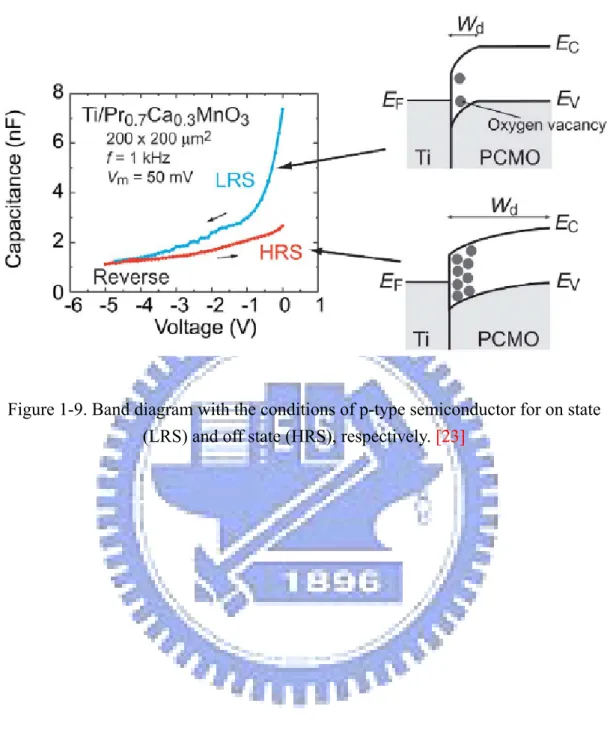
Figure 2.1. Schematic diagram of Ti/TiN/SiO2/PtFe/SiO2/Si structure, and its small
•
•
P
P
-
-
type Si
type Si
(100) substrate
(100) substrate
•
•
Wet oxidation (500nm)
Wet oxidation (500nm)
•
•
FePt
FePt
(50nm)
(50nm)
•
•
50nm PECVD oxide
50nm PECVD oxide
•
•
RCA clean
RCA clean
•
•
30nm TiN and 80nm Ti deposition by
30nm TiN and 80nm Ti deposition by
sputtering, then TiN
sputtering, then TiN
\
\
Ti patterning & etching
Ti patterning & etching
•
•
P
P
-
-
type Si
type Si
(100) substrate
(100) substrate
•
•
Wet oxidation (500nm)
Wet oxidation (500nm)
•
•
FePt
FePt
(50nm)
(50nm)
•
•
50nm PECVD oxide
50nm PECVD oxide
•
•
RCA clean
RCA clean
•
•
30nm TiN and 80nm Ti deposition by
30nm TiN and 80nm Ti deposition by
sputtering, then TiN
sputtering, then TiN
\
\
Ti patterning & etching
Ti patterning & etching
•
•
P
P
-
-
type Si
type Si
(100) substrate
(100) substrate
•
•
Wet oxidation (500nm)
Wet oxidation (500nm)
•
•
50nm Fe
50nm Fe
0.730.73Pt
Pt
0.270.27(composition by ICP
(composition by ICP
-
-
MS)
MS)
•
•
50nm PECVD oxide deposition and 30nm TiN
50nm PECVD oxide deposition and 30nm TiN
deposition by sputtering, then TiN patterning & etching
deposition by sputtering, then TiN patterning & etching
•
•
RCA clean
RCA clean
•
•
200nm Via hole and 250nm contact hole, then
200nm Via hole and 250nm contact hole, then
80nm Ti lithography patterning and etching
80nm Ti lithography patterning and etching
(100um
(100um
×
×
100um)
100um)
•
•
P
P
-
-
type Si
type Si
(100) substrate
(100) substrate
•
•
Wet oxidation (500nm)
Wet oxidation (500nm)
•
•
50nm Fe
50nm Fe
0.730.73Pt
Pt
0.270.27(composition by ICP
(composition by ICP
-
-
MS)
MS)
•
•
50nm PECVD oxide deposition and 30nm TiN
50nm PECVD oxide deposition and 30nm TiN
deposition by sputtering, then TiN patterning & etching
deposition by sputtering, then TiN patterning & etching
•
•
RCA clean
RCA clean
•
•
200nm Via hole and 250nm contact hole, then
200nm Via hole and 250nm contact hole, then
80nm Ti lithography patterning and etching
80nm Ti lithography patterning and etching
(100um
(100um
×
×
100um)
100um)
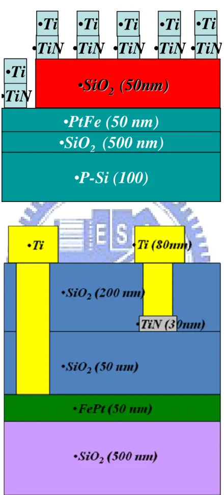
Figure 2.2. Process flows of Ti/TiN/SiO2/PtFe/SiO2/Si structure, and its small size
Chapter 3
Results and discussions
In this chapter, four sections will be discussed. All of the devices are applied voltage in bottom electrodes, and the top electrodes are ground (Fig. 3-1).
(a) Device structures and characteristics.
(b) Bottom electrode metal effect.
(c) Thermal treatment effect.
(d) Small size effect.
3.1 Device Structures and Characteristics
In section 3.1, the resistive switching properties of different structures are examined and divided into three parts, including results of various bottom electrode metals, various top electrode metals, and various SiO2 thickness.
3.1.1 Various bottom electrode metals
First of all, the resistive switching phenomenon is studied in Al (400nm) / SiO2
(50nm) / Pt (50nm) structure and its depiction of process flows in Fig. 3-2 and Fig.
3-3. The initial state of as deposition Al / SiO2 / Pt structure processes high resistance
value before forming process (Fig. 3-4). It should be noted that, in the previous
the Al/SiO2/Pt structure in my thesis does not possess resistance switching phenomena
after the forming process (Fig. 3-5).
In order to study resistance switching behavior for SiO2 on alloy electrode, the Al
(400nm) / SiO2 (50nm) / PtFe (50nm) is fabricated. Its structure and process flows are
depicted in Fig. 3-6 and Fig. 3-7. Unlike Al / SiO2 / Pt structure, the Al / SiO2 / PtFe
structure processes stably and repetitively resistance switching behaviors after the
forming process (Fig. 3-8). In order to clarify the mechanisms of resistance switching
behavior, seven parts will be discussed in this section.
3.1.1.1 Mechanism of Forming Process
The forming process means that the application of a large voltage a will soften the breakdown of a device. In order to avoid the device being permanent damage, the measurement parameter would set a compliance current which is controlled by a
feedback system in apparatus, like Fig. 3-9. A large voltage would produce a high
electrical field which induces impact ionization breakdown (Fig. 3-10) in SiO2 for Al /
SiO2 / Pt structure [25]. Hence, there are many low resistance paths produced, like
Fig. 3-11.
For the Al / SiO2 / PtFe structure, it is at initial state and processes high
resistance value before forming process (Fig. 3-12). During the forming process (Fig.
3-13), bottom PtFe electrode is applied in a large negative voltage which will produce
a high electrical field. Hence, the breakdown of impact ionization would happen in SiO2 and Fe2O3 which is formed on PtFe alloy electrode during the fabrication process
(Fig. 3-14). Then, there are many low resistance paths produced in SiO2, and an
would be continued and its related switching mechanisms are similar with the set process.
3.1.1.2 Mechanism of Phase Change in the Reset Process
After the set and forming process, reset process is the second step to switch resistance. The reset process is that the bottom electrode applies positive voltage, and the top electrode is grounding, like Fig. 3-1. Due to the electrical field direction (Fig.
3-16) and high current flowed through the “electric faucet” [37], the oxygen ion and
localization Joule heating (Fig. 3-17) [39] cause the phase change of Fe3O4 (Fig. 3-18)
which is formed during the forming or set process. The chemical reaction possesses relationship as following [18]:
2 Fe3O4 + O2- => 3 Fe2O3 + 2 e
-The resistance between Fe2O3 and Fe3O4 is different because the band gap of
Fe2O3 and Fe3O4 are 2.6eV and 1.6eV, respectively [40, 41]. The total resistance of the
insulating layer is the low resistance paths in SiO2 series connection with Fe2O3 thin
film which is less conductive. Hence, the phase change from Fe3O4 to Fe2O3 would
switch the current or resistance from LRS to HRS in the process of reset.
3.1.1.3 Mechanism of Oxygen Vacancies in the Reset Process
To affect resistance switching behavior is another factor, the amounts of oxygen vacancies. Reset process follows the step of the set or following process. The voltage sweep mode is also the same with Fig. 3-1. Due to the electrical field direction (Fig.
3-16) and high current flowed through the “electric faucet” [37], the oxygen ion and
localization Joule heating (Fig. 3-17) [39] would decrease the amounts of oxygen
process. The chemical reaction possesses relationship as following [23]:
V’’ (donor) + O2- => O
Due to oxygen vacancies could be seen as donor type defects [23], they would
supply electron concentrations in the intrinsic n-type Fe2O3 semiconductor (further
discussion about band diagram would be continued in the next section) [38]. The less
amounts of oxygen vacancies exist at the electric faucet, the less conductive paths would form. Therefore, after the reset process, the total resistance of the insulating
layer is the low resistance paths in SiO2 series connection with less oxygen vacancies
of Fe2O3 thin film which is less conductive. The amounts of oxygen vacancies that are
decreased in the intrinsic n-type Fe2O3 semiconductor would switch the current or
resistance from LRS to HRS during the reset process.
3.1.1.4 Band diagram in the Reset Process
During the reset process, the phase change of Fe2O3 and oxygen vacancies both
play important roles in causing resistance switching. After reset process, the band
diagram of intrinsic n-type Fe2O3 semiconductor shows in Fig. 3-19. Finally, the
Frenkel-Poole emission is predicted by current fitting with different temperature (shows in section 3.3.4) (Fig. 3-20).
3.1.1.5 Mechanism of Phase Change in the Set Process
After the reset process, set process is the second step to switch resistance. The set process is that the bottom electrode applies negative voltage, and the top electrode is
grounding, like Fig. 3-1. Due to the electrical field direction (Fig. 3-21) and the
applied power by measurement system, the electric faucet would be opened [37]. That
chemical reaction possesses relationship as following [18]:
2 Fe3O4 + O2- <= 3 Fe2O3 + 2 e
-Due to band gap differences between Fe2O3 and Fe3O4, the total resistance of the
insulating layer is the low resistance paths in SiO2 series connection with Fe3O4 thin
film which is conductive. Hence, the phase change from Fe2O3 to Fe3O4 would switch
the current or resistance from HRS to LRS during the set process.
3.1.1.6 Mechanism of Oxygen Vacancies in the Set Process
The role of Oxygen Vacancies is also an important factor to cause resistance switching. First, the set process is the following step to switch resistance after reset
process. The voltage sweep mode is also the same with Fig. 3-1. Due to the electrical
field direction (Fig. 3-21) and the applied power by measurement system, the electric
faucet would be opened in Fe2O3 after forming or set process [37]. The reason is that
the amounts of oxygen vacancies would increase in some regions, and these regions represent highly conductive paths in Fe2O3 thin film. The chemical reaction possesses
relationship as following [23]:
V’’ (donor) + O2- <= O
From the previous sections, oxygen vacancies could be seen as donor type defects, which could supply electron (donor) concentrations in the intrinsic n-type
Fe2O3 semiconductor (further discussion about band diagram would be continued in
the following section) [38]. The more amounts of oxygen vacancies exist at the
electric faucet, the more conductive paths would form. Hence, after the set process, the total resistance of the insulating layer is the low resistance paths in SiO2 series
connection with many oxygen vacancies of Fe2O3 thin film which is highly
conductive. The amounts of oxygen vacancies increased in the intrinsic n-type Fe2O3
semiconductor would switch the current or resistance from HRS to LRS during reset process.
3.1.1.7 Band diagram in the Set Process
During the set process, the phase change of Fe2O3 and oxygen vacancies both
play important roles to cause resistance switching. After set process, the band diagram of enhanced n-type Fe2O3 semiconductor shows in Fig. 3-23. Finally, the tunneling is
predicted by current fitting with different temperature, where the current is less temperature sensitive at LRS (shows in section 3.3.4) (Fig. 3-24).
3.1.2 Effects of Top Electrode Metal Effects
In order to clarify where the key point to cause resistance switching is from, there were many studies had been done before. Therefore, many possible models have
been proposed to explain where resistance switching occurred [28]. From the 3.1.1
section, the bottom PtFe electrode is the key point to cause resistance switching. Hence, in order to prove that two different top electrode metals (Al (400nm) and Ti (80nm) / TiN (30nm) ) are fabricated, and using W probe becomes top electrode with the utmost care that tip does not scratch or perforate the oxide surface. The bistable
resistance switching properties have been found in these three structures (Fig. 3-25
(a)-(c)). These evidences show that the top electrode region is not the dominant factor
to cause resistance switching. Furthermore, work function difference (TiN: 4.8~5.3 eV; W: 4.5 eV; Al: 4.1 eV) in some cases would affect the resistance switching behavior,
like contact between metal and p-type or n-type semiconductor [32, 33]. However,
affect the resistance switching behavior about the electrode/SiO2/PtFe structure.
3.1.3 Effects of SiO
2Thicknesses
The final part wants to discuss different SiO2 thickness effects. Two different
structures have been fabricated, and they only adjust SiO2 thickness (50nm and 30nm)
in both structures (Fig. 3-26 (a)-(b)). In order to let them possess bistable resistance
switching characteristics, forming process must do in both structures. From the electrical results, both structures need the same forming electric field (~5MV/cm) to
let devices possess bistable resistance switching (Fig. 3-27 (a)-(b)). These phenomena
indicated that SiO2 thickness would not affect resistance switching properties, and
they only affect forming process (voltage amplitude) which lets SiO2 thin film
produces impact ionization breakdown.
3.1.4 Summary I
From the above analysis, we could conclude three points to cause resistance switching characteristics from these different structures.
(a) Bottom electrode contains Fe elements play an important role to cause bistable resistance switching. Proposed models and mechanisms about
electric faucet, Redox of Fe2O3, oxygen vacancies, and band diagram could
explain the bistable resistance switching behavior.
(b) In the SiO2/FePt system, the resistive memory switching phenomena are
independent of top electrode metal effects.
(c) SiO2 thickness effects do not affect resistance switching behaviors when it
3.2 Effects of Bottom Electrode Metals
In order to understand more details about resistance switching characteristics for
Ti/TiN/SiO2/PtFe structure, the Ti/TiN/SiO2/Fe/Pt/Ti structure is also fabricated to
demonstrate why the Ti/TiN/SiO2/FePt structure possesses resistance switching
characteristics. Both structures and process flows show in Fig. 3-28 (a)-(c). It is
interesting that the original structure (electrode/SiO2/Pt) does not possess resistance
switching behavior. However, if the original structure is inserted by a thin Fe film
between SiO2 and Pt, this modified structure comes to possess bistable resistance
switching property.
3.2.1 Electrical properties
3.2.1.1 Bistable Resistance switching
Fig. 3-29 (a)-(b) are bistable resistance switching characteristics for
Ti/TiN/SiO2/FePt and Ti/TiN/SiO2/Fe/Pt/Ti structures. The forming process needs
between both structures, and the forming electrical field is 5.13MV/cm and
5.46MV/cm respectively. According to 3.1.3 section analysis, SiO2 thickness will not
affect resistance switching properties, and they only affect forming process (voltage
amplitude) which lets SiO2 thin film produces impact ionization breakdown. Hence,
forming electrical field is almost the same between both structures. There is another key point behind these phenomena that is the interfacial Fe element that can cause
resistance switching behavior (The original structure of electrode/SiO2/Pt does not
3.2.1.2 Current-Voltage Fitting
Fig. 3-30 shows the current-voltage fitting results of Ti/TiN/SiO2/FePt and
Ti/TiN/SiO2/Fe/Pt/Ti structures. There are three important points in this result.
First, at low resistance state, the current transports of both structures are similar and the fitting results are Ohmic law (Slope of ln (I) vs. ln (V) curve is 1).
Second, at high resistance state low voltage bias region, the current transports of both structures are also similar and the fitting results are Ohmic law (Slope of ln (I) vs. ln (V) curve is 1).
Third, at high resistance state high voltage bias region, the current transports of both structures are similar again, and the fitting results are close to Frenkel-Poole emission (the relationship of ln (J/V) vs. V1/2 curve is linear).
From the current-voltage fitting results, indicated that both of structures
(Ti/TiN/SiO2/FePt and Ti/TiN/SiO2/Fe/Pt/Ti) possess the similar current transport
characteristics.
3.2.1.3 I-V Characteristics Distribution
Fig. 3-31 (a)-(c) depicts that set (reset) voltage, set (reset) current and set (reset)
power dissipation for the both structures. All the statistics results are extracted from five samples and 300 times bistable resistance switching per sample.
From the set and reset voltage distribution, PtFe bottom electrode structure need less value to cause resistance switching than Fe bottom electrode structure (area is
![Figure 1-1. Typical linear I-V curves of RRAM switching in voltage sweeping mode (unipolar) [23]](https://thumb-ap.123doks.com/thumbv2/9libinfo/8558740.188413/27.892.150.739.128.1062/figure-typical-linear-curves-switching-voltage-sweeping-unipolar.webp)

![Figure 1-7. Schematic of the filament in an oxide. [28]](https://thumb-ap.123doks.com/thumbv2/9libinfo/8558740.188413/30.892.140.755.153.953/figure-schematic-filament-oxide.webp)
![HPSH [ 氧化數平衡反應式係數 ]](data:image/gif;base64,R0lGODlhAQABAIAAAP///wAAACH5BAEAAAAALAAAAAABAAEAAAICRAEAOw==)