IEEE ELECTRON DEVICE LETTERS, VOL. 31, NO. 11, NOVEMBER 2010 1227
In-Plane Gate Transistors Fabricated by Using
Atomic Force Microscopy Anode Oxidation
Tung-Hsun Chung, Shu-Han Chen, Member, IEEE, Wen-Hsuan Liao, and Shih-Yen Lin, Member, IEEE
Abstract—An in-plane gate transistor fabricated by using the
atomic force microscopy (AFM) lithography is investigated in this letter. By performing repeated oxidation and deoxidation proce-dures by using the AFM for four times, two V-shaped trenches are fabricated on the prepatterned mesas to isolate the electrical terminals of the device. Without exposing the channel region to the atmosphere, the device has exhibited standard transistor current–voltage characteristics in the 0–5 V range at room tem-perature, which may be advantageous for the future high-speed application of the device.
Index Terms—Atomic force microscopy (AFM), in-plane gate
transistors.
I. INTRODUCTION
T
O ACHIEVE a higher transistor density over a single wafer in the Si industry, the photolithography technology has been rapidly developed from 0.18 μm to the current 45-nm nodes. However, with the reduced device sizes, issues like the huge gate leakage currents with thin SiO2gate dielectrics and the limitation of the photolithography technology have arisen [1]. To overcome the problem of the huge leakage currents resulting from the thin gate dielectrics, one approach is to develop high-κ materials to replace the SiOxgate dielectrics.The other approach would be the development of new transistor structures without the requirement for the gate dielectrics. To achieve this goal, one possible candidate would be the in-plane gate transistor [2]. The source, drain, and gate terminals of this device structure are located on the same plane. By using e-beam lithography to fabricate the electrical isolations between the electrical terminals, the conductivity of the 2-D electron gas (2DEG) channel could be modulated by the in-plane gates such that the transistor behaviors could be observed [2], [3]. Although the device is easy to fabricate, the adoption of e-beam technology has made this approach complicated and expensive. An alternate approach to provide the electrical isolations
be-Manuscript received July 25, 2010; revised August 4, 2010; accepted August 5, 2010. Date of publication September 27, 2010; date of current version October 22, 2010. This work was supported in part by the National Science Council, Taiwan, under Grants NSC 99-2628-E-001-001 and NSC 99-2911-I-001-010. The review of this letter was arranged by Editor M. Passlack.
T.-H. Chung, S.-H. Chen, and W.-H. Liao are with the Research Center for Applied Sciences, Academia Sinica, Taipei 11529, Taiwan (e-mail: [email protected]; [email protected]; dwater21@ hotmail.com).
S.-Y. Lin is with the Research Center for Applied Sciences, Academia Sinica, Taipei 11529, Taiwan, the Department of Photonics, National Chiao Tung University, Hsinchu 300, Taiwan, and also with the Institute of Optoelectronic Sciences, National Taiwan Ocean University, Keelung 20224, Taiwan (e-mail: [email protected]).
Color versions of one or more of the figures in this letter are available online at http://ieeexplore.ieee.org.
Digital Object Identifier 10.1109/LED.2010.2068273
tween terminals and leave nanometer-size channels would be the atomic force microscopy (AFM) lithography (AFML). In a previous report, the transistors with in-plane gates fabricated by using the AFML operated at low temperatures have already been demonstrated [4].
In this letter, a transistor with in-plane gates fabricated by using the AFML is investigated. By performing repeated oxida-tion and deoxidaoxida-tion procedures by using AFM for four times, two V-shaped trenches could be fabricated on the prepatterned mesas. Although the trenches fabricated by using this method do not penetrate through the 2DEG channel, the electrical isolations could still be established between the terminals. The phenomenon is attributed to the depletion-induced isolations resulting from the surface-state pinning on the trench sidewalls. Without exposing the channel region to the atmosphere, the device has exhibited standard transistor current–voltage char-acteristics in the 0–5 V range at room temperature.
II. EXPERIMENTS
The wafer discussed in this letter is prepared by RIBER C21 solid-source molecular beam epitaxy. A structure consists of a 30-nm Si-doped GaAs capping layer, a 15-nm Si-doped Al0.3Ga0.7As donor layer, a 15-nm undoped Al0.3Ga0.7As spacing layer, and a 200-nm buffer layer grown on a semi-insulating GaAs substrate. The doping densities for the n-type GaAs and Al0.3Ga0.7As layers are 1.67× 10¹⁸ and 1.15× 1018 cm−3, respectively. The Hall measurement shows that the room-temperature sheet carrier density and the elec-tron mobility of the 2DEG channel formed in the undoped GaAs/Al0.3Ga0.7As interface are 5.3× 1011 cm−2 and 5.7× 103 cm2/v· s, respectively. Before the channel definition by
the AFML, a crisscross mesa with a width/depth of 20/0.1 μm is fabricated at first by using standard photolithography. The metal electrodes with Ohmic contacts to the n-type GaAs capping layer are deposited at the four ends of the crisscross mesa. The Veeco Innova AFM system is adopted for either the AFML or AFM applications in this letter. The PtIr5-coated Si tips with a cantilever spring constant of 0.2 N/m are employed for local anode oxidation (LAO) in a contact mode with an ac voltage of 10.0 V at 1 kHz [5]. For each deoxidation procedure, the wafer is dipped into 3.7% HCl aqueous solution for 90 s [6].
III. RESULTS ANDDISCUSSIONS
The first issue to be investigated is the depth required for the trenches to reach the electrical isolations between the terminals. According to the results obtained on the GaAs substrates, the average trench depth for a given oxidation/deoxidation
1228 IEEE ELECTRON DEVICE LETTERS, VOL. 31, NO. 11, NOVEMBER 2010
Fig. 1. Trench depth and corresponding electrical resistance between two electrodes with different oxidation/deoxidation times.
Fig. 2. Top view of the device observed under an optical microscope. The insert shows the 1× 1 μm2AFM image of the device at the channel region.
procedure is∼10–20 nm. Considering that the total layer thick-ness above the 2DEG channel is 60 nm, repeated oxidation/ deoxidation procedures are expected to achieve electrical iso-lations for the structure. The trench depth and correspond-ing electrical resistance between two electrodes with different oxidation/deoxidation times are shown in Fig. 1. As shown in the figure, a linear dependence of the trench depth with oxidation/deoxidation times is observed for the sample. How-ever, a sudden increase of the resistance from hundreds of kiloohms to several megaohms is observed after the fourth oxidation/deoxidation procedure. The trench width obtained after four times of the oxidation/deoxidation procedure is
∼200 nm. Since the trench depth after four oxidation/
deoxidation times is only∼45 nm, which is 15 nm above the 2DEG channel, the results suggest that, even if the trench does not penetrate through the 2DEG channel, the electrical isola-tions could still be achieved. The phenomenon is attributed to the depletion-induced isolations between the electrodes, which is resulted from the surface-state pinning of the trenches [7].
Based on the results discussed earlier, a transistor with in-plane gates is fabricated on this structure. Four oxidation/ deoxidation times are adopted to fabricate the trenches to isolate the four electrical terminals. The top view of the device under an optical microscope is shown in Fig. 2. The AFM image of
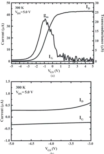
Fig. 3. (a) Room-temperature ID, IG, and gmversus the VGScharacteristics
at VGS=−5−5 V. (b) The IDand IGcurves at VGS=−3 to − 5 V of the
device at a fixed VDSof 5.0 V.
the device showing the channel region is shown in the insert of the figure. The designed channel width and length of the device are 650 and 500 nm, respectively. As shown in the figure, abrupt trenches and a well-defined channel are observed for the device. The results have demonstrated great repeatability of the AFM LAO at the same position. As discussed in the last paragraph, the trench depth is around 45–50 nm, which is 15 nm above the location of the 2DEG channel. In other words, the trenches do not penetrate through the 2DEG channel.
The room-temperature drain current (ID)-versus-gate–
source voltage (VGS) characteristics of the device at a fixed drain–source voltage (VDS) of 5.0 V are shown in Fig. 3(a). The corresponding IG and derived transconductance (gm) curves
are also shown in the figure. As shown in the figure, the obvious
ON/OFFdifference is observed from the ID–VGScurve. The de-vice is turned off when VGSis lower than−3.0 V and saturated when VGSis higher than 2.0 V. The results suggest that, when a negative VGS is applied, the electrons in the 2DEG channel would be depleted. The channel is fully depleted of electrons when VGS is lower than −3.0 V. In this case, the device is in theOFFstate. When a positive VGSis applied to this device, the depletion regions in the device channel which is resulted from the surface-state pinning near the trench sidewalls would be gradually compensated by the injected ID currents. When
CHUNG et al.: IN-PLANE GATE TRANSISTORS FABRICATED BY USING AFM ANODE OXIDATION 1229
Fig. 4. Room-temperature ID–VDS curves of the device at VGS=
−5.0, 0.0, and 5.0 V.
VGS is higher than 2.0 V, the 2DEG channel would be fully opened. In this case, the device is in theONstate. The
transcon-ductance of the device derived through the ID–VGScurve has shown a maximum value of 20 μS, which is much smaller than that of the conventional transistors. The phenomenon is attributed to the long and wide channel of the crisscross mesa. A reduction in the source/drain electrode distance is necessary in the future to reduce the series resistance. The air-bridge process may also help to reduce the parasitic capacitance below the metal [8]. In this case, the effective device area can be reduced, which is advantageous for the high-speed operation of this device.
Moreover, shown in Fig. 3(a) are the gate currents (IG) under
different VGS’s. When the device is under theONstate, the low gate currents suggest that, even if the trenches do not penetrate through the 2DEG channel, the electrical isolations between the terminals could still be achieved with the electron depletion in the 2DEG channel which is resulted from the surface-state pinning. However, when the device is in theOFFstate, IDand IG are of the same value but with different signs. The ID and IG curves of the device at VGS=−3 to − 5 V are shown in Fig. 3(b). The results suggest that the leakage current is mainly from the gate terminals. In this case, although the trenches may act as electrical isolations in theONstate, the leakage currents from the gates are still observed in the OFF state since the trenches do not penetrate through the 2DEG channel.
The room-temperature ID–VDS curves of the device at
VGS=−5.0, 0.0, and 5.0 V are shown in Fig. 4. As shown in the figure, standard transistor curves with flat saturation regions are observed for this device. The ON/OFFratio of the device at VGS= 5.0 and− 5.0 V and VDS= 5.0 V has reached 290. Further improvement in thinning the layer structures to enhance the electrical isolation with a fixed trench depth may help to increase the ON/OFF ratio in the future. The other remaining issue is the actual channel width of the device. Since the surface-state pinning effect plays an important role in the electrical isolation for the terminals, the effect would also influence the actual channel width of the device. Since
the 2DEG channel is not exposed to the atmosphere for this device, the electron mobility and the sheet carrier density in the channel could be assumed to be the same as the value obtained by the Hall measurements. In this case, by using the equation
R = L/(qμnNDW ), where R is the resistance of the device
at the linear region, μn and ND are the electron mobility and
the sheet carrier density, respectively, and L and W are the channel length and channel width, respectively, an estimate of the effective channel width could be obtained [9]. The effective channel width of the device obtained by using this equation at VGS= 0 V is 13.7 nm, assuming that the channel length is 500 nm. Although the resistance contribution of the crisscross mesa is not excluded in this calculation, the results suggest that the depletion region would spread 200–300 nm into the channel region from a single side of the trench. The results have pro-vided a supporting evidence that the electrical isolation could be achieved through the electron depletion which resulted from the surface-state pinning when the trenches do not penetrate through the 2DEG channel.
IV. CONCLUSION
In conclusion, a transistor with in-plane gates fabricated by using the AFML is investigated. Without exposing the channel region to the atmosphere, the device has exhibited standard transistor current–voltage characteristics in the 0–5 V range at room temperature, which may be advantageous for the future high-speed application of the device. The development of this device is advantageous for the practical applications of nanodevices.
REFERENCES
[1] M. Ieong, B. Doris, J. Kedzierski, K. Rim, and M. Yang, “Silicon device scaling to the sub-10-nm regime,” Science, vol. 306, no. 5704, pp. 2057– 2060, Dec. 2004.
[2] A. D. Wieck and K. Ploog, “In-plane-gated quantum wire transistor fabri-cated with directly written focused ion beams,” Appl. Phys. Lett., vol. 56, no. 10, pp. 928–930, Mar. 1990.
[3] J. Nieder, A. D. Wieck, P. Grambow, H. Lage, D. Heitmann, K. v. Klitzing, and K. Ploog, “One-dimensional lateral-field-effect transistor with trench gate-channel insulation,” Appl. Phys. Lett., vol. 57, no. 25, pp. 2695–2697, Dec. 1990.
[4] R. Held, T. Vancura, T. Heinzel, K. Ensslin, M. Holland, and W. Weschedier, “In-plane gates and nanostructures fabricated by direct oxidation of semiconductor heterostructures with an atomic force micro-scope,” Appl. Phys. Lett., vol. 73, no. 2, pp. 262–264, Jul. 1998.
[5] J. A. Dagata, T. Inoue, J. Itoh, K. Matsumoto, and H. Yokoyama, “Role of space charge in scanned probe oxidation,” J. Appl. Phys., vol. 84, no. 12, pp. 6891–6900, Dec. 1998.
[6] M. Bartošík, D. Škoda, O. Tomanec, R. Kalousek, P. Jánský, J. Zlámal, J. Spousta, and T. Šikola, “The influence of humidity on the kinetics of local anodic oxidation,” J. Phys., Conf. Ser., vol. 61, no. 61, pp. 75–79, 2007.
[7] H. van Houten, B. J. van Wees, M. G. J. Heijman, and J. P. Andre, “Submicron conducting channels defined by shallow mesa etch in GaAs-AlGaAs heterojunctions,” Appl. Phys. Lett., vol. 49, no. 26, pp. 1781–1783, Dec. 1986.
[8] W. Snodgrass, B. R. Wu, K. Y. Cheng, and M. Feng, “Type-II GaAsSb/InP DHBTs with record fT = 670 GHz and simultaneous fT, fMAx>
400 GHz,” in IEDM Tech. Dig., 2007, pp. 663–666.
[9] S. M. Sze and K. K. Ng, Physics of Semiconductor Devices. Hoboken, NJ: Wiley-Interscience, 2007, ch. 1.