This content has been downloaded from IOPscience. Please scroll down to see the full text.
Download details:
IP Address: 140.113.38.11
This content was downloaded on 28/04/2014 at 18:50
Please note that terms and conditions apply.
Fabrication and resistive switching characteristics of high compact Ga-doped ZnO nanorod
thin film devices
View the table of contents for this issue, or go to the journal homepage for more 2012 Nanotechnology 23 145201
(http://iopscience.iop.org/0957-4484/23/14/145201)
Nanotechnology 23 (2012) 145201 (8pp) doi:10.1088/0957-4484/23/14/145201
Fabrication and resistive switching
characteristics of high compact Ga-doped
ZnO nanorod thin film devices
I-Chuan Yao
1, Dai-Ying Lee
2, Tseung-Yuen Tseng
2and Pang Lin
11Department of Materials Science and Engineering, National Chiao Tung University, Hsinchu 300,
Taiwan
2Department of Electronics Engineering and Institute of Electronics, National Chiao Tung University,
Hsinchu 300, Taiwan E-mail:[email protected]
Received 4 December 2011, in final form 13 February 2012 Published 21 March 2012
Online atstacks.iop.org/Nano/23/145201
Abstract
This study investigates the resistive switching behavior of Ga-doped ZnO (GZO) nanorod thin films with various Ga/Zn molar ratios. Vertically well-aligned and uniform GZO nanorod thin films were successfully grown on Au/Ti/SiO2/p-Si substrates using an aqueous solution
method. X-ray diffraction (XRD) results indicate that GZO nanorods have [0001] highly preferred orientation. Scanning electron microscopy (SEM) and transmission electron
microscopy (TEM) observations show the formation of highly ordered and dense nanorod thin films. These compact GZO nanorod thin films can be used to make resistive switching memory devices. Such memory devices can be reversibly switched between ON and OFF states, with a stable resistance ratio of ten times, narrow dispersion of ON and OFF voltages, and good endurance performance of over 100 cycles. The resistive switching mechanism in these devices is related to the formation and rupture of conducting filaments consisting of oxygen vacancies, occurring at interfaces between GZO nanorods (grain boundaries). Results show that the resulting compact GZO nanorod thin films have a high potential for resistive memory applications.
(Some figures may appear in colour only in the online journal)
1. Introduction
Next-generation nonvolatile memory (NVM) has attracted increasing attention as conventional charge-storage-based flash memories approach their scaling limits. To overcome this significant issue, researchers have examined various emerging NVMs, including ferroelectric random access memory, phase-change random access memory, magnetic random access memory and resistance random access memory (RRAM), as replacements for flash memory. Previous studies have indicated that RRAM is a promising candidate because of its simple structure, high operational speed and high density integration. Researchers have proposed a number of metal oxides, including ZrO2 [1–5],
TiO2 [6–8], Pr1−xCaxMnO3 [9], SrZrO3 [10,11], ZnO [12,
13] and NiO [14] for RRAM applications because of their
excellent characteristics. Among these, the ZnO-based film is one of the most attractive materials for RRAM applications because of its high transparency, reliability and stable resistive switching (RS) behavior of the metal–insulator–metal (MIM) structure [12, 13]. Chang et al prepared RS devices by aligning ZnO nanorods on an ITO substrate using a low-temperature chemical solution method [15]. Yang et al fabricated a single Sb-doped ZnO nanobelt/SiOx/p-Si
device exhibiting RS behavior, as measured by atomic force microscopy (AFM) [16]. Compared with thin film RS devices, a 1D nanostructure can provide a localized conducting filament in devices that allow RS operation with a narrow dispersion of operational parameters. However, direct contact between the top and bottom electrodes may cause a short circuit problem if the top electrode is fabricated on a ZnO nanorod resistive switching film with a low packing density.
c
Nanotechnology 23 (2012) 145201 I-C Yao et al
Figure 1. Schematic structure of the Au/GZO nanorod thin film/ZnO/Au device structure.
A hybrid RS device consisting of ZnO nanorods embedded in insulating polymethylmethacrylate (PMMA) polymer can avoid such direct contact [17]. However, embedding ZnO nanorods in PMMA is a complex and time-consuming process. Preparing high density and high compact ZnO nanorod thin films without an additional polymer-embedded process is highly advantageous for RS devices.
This study develops a simple process of forming continuous and extremely dense Ga-doped ZnO (GZO) nanorod thin films with a highly preferred orientation on Au/Ti/SiO2/p-Si substrates from a low-temperature aqueous
solution. This study also investigates the RS behavior and conduction mechanisms of nanorod thin films without any embedding. Results demonstrate that the films exhibit excellent bipolar RS behavior, including low operational voltage and good endurance property.
2. Experimental details
Figure 1 shows a schematic view of the GZO nanorod-array-based memory device. A 79.30 ± 1.54 nm thick ZnO buffer layer was first deposited on a Au/Ti/SiO2/Si substrate
by radio-frequency (RF) magnetron sputtering. The aqueous synthesis of GZO nanorods was subsequently conducted at 90◦C in a sealed kettle placed in a quartz beaker. The ZnO-coated substrates were immersed in precursor solutions of zinc chloride (0.025 M), ammonium hydroxide solution (25%) and gallium chloride (Ga/Zn molar ratios of 0, 6, 8 and 10%) for 10 min. The chemical composition of the GZO nanorods and the pH value in the deposition solution were controlled by adjusting the Ga/Zn molar ratio (table1). After the formation reaction, the substrates were removed from the solution, thoroughly rinsed with deionized water and dried in air. To achieve the MIM structure, 80 nm thick Au top electrodes with diameters of 150, 250 and 350 µm were deposited by electron beam evaporation using a shadow mask. The morphology, size distribution and crystal structure
Table 1. Relationship of Ga/Zn molar ratio in solution, pH of the solution and real Ga/Zn atomic ratio in GZO nanorod.
Device no. Ga/Zn molar ratio in solution (%) pH value of solution
Real Ga/Zn molar ratio of GZO nanorods based on EDS analyzed results (%) Device 1 0 7.0 ± 0.2 0 Device 2 6 9.0 ± 0.2 6.06 ± 0.24 Device 3 8 9.3 ± 0.1 7.44 ± 0.47 Device 4 10 9.4 ± 0.1 9.00 ± 0.31
of the GZO nanorods were examined by field-emission scanning electron microscopy (FE-SEM, Hitachi S-4700I), transmission electron microscopy (TEM, JEOL 2100F) and an x-ray diffractor (XRD, Bede D1), respectively. The TEM specimen was prepared by a focused-ion beam (FIB, FEI Nova 200). To prove the chemical composition, a line-scan mapping was executed by an energy dispersive x-ray spectrometer (EDS, Oxford ISIS300). Photoluminescence (PL) spectroscopy was employed at room temperature using a 325 nm He–Cd laser for the optical characterization of the GZO nanorod thin films with various Ga/Zn molar ratios. The current–voltage (I–V) characteristics of all GZO devices were measured by an Agilent 4155C semiconductor parameter analyzer at room temperature.
3. Results and discussion
3.1. Morphology and crystalline structure
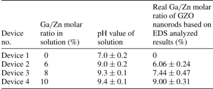
Figures 2(a)–(d) show typical FE-SEM images of GZO nanorod thin films with various Ga/Zn molar ratios synthe-sized for 10 min using the solution method. The vertically well-aligned nanorods were grown on the Au/Ti/SiO2/Si
substrate and the diameter of the nanorods increased from 50.9 ± 19.4 to 101.5 ± 26.4 nm as the Ga/Zn molar ratio increased from 0 to 10% in the deposition solutions (insets in figures2(a)–(d), respectively). The thickness of the nanorod films was approximately 220 nm. A low packing density nanorod film was formed on the substrate in the solution without Ga doping (device 1), whereas increasingly dense nanorod array films were formed on the substrates in deposition solutions with Ga/Zn molar ratios increasing from 6 to 10% (devices 2, 3 and 4, respectively). These different morphologies may arise from different nucleation and growth processes, because of different interfacial energies between the ZnO buffer layer and different-composition GZO nanorods [18]. The direct contact between top and bottom electrodes occurred in the highly porous nanorod film without Ga (device 1; figure2(a)), leading to the short circuit problem. The RS behavior was not observed in this device according to DC voltage sweeping (I–V) measurement.
Figure 3(a) shows the XRD patterns of GZO nanorod thin films with various Ga/Zn molar ratios, indicating that all the nanorod thin films exhibit a single phase with a wurtzite structure and have (002) highly preferred orientation (space group P63mc; JCPDS card no. 36-1451). These XRD
Figure 2. Typical FE-SEM cross sectional images of (a) device 1, (b) device 2, (c) device 3 and (d) device 4; (insets of (a)–(d) are top view of devices 1, 2, 3 and 4, respectively).
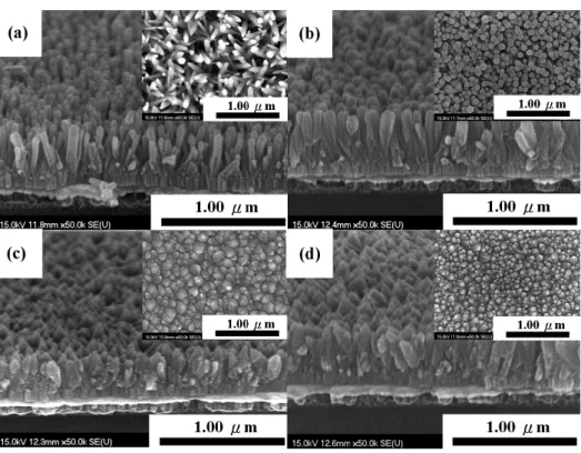
patterns show no peak corresponding to gallium or gallium oxide. The peaks marked with Au(002), (111) and (220) belong to the Au electrode. The XRD pattern of the nanorod film without Ga doping has a higher intensity (002) peak than other nanorod films, indicating that such a nanorod has better crystallinity than Ga-doping nanorods. The lattice constants of GZO (molar ratio = 0, 6, 8 and 10% in deposition solution) nanorods are a = b = ∼3.256 ˚A, c = ∼5.204 ˚A; a = b = ∼3.255 ˚A, c = ∼5.198 ˚A; a = b = ∼3.252 ˚A, c = ∼5.194 ˚A and a = b = ∼3.252 ˚A, c = ∼5.191 ˚A, respectively (figure 3(b)). These values can be calculated according to the XRD patterns. As the Ga/Zn molar ratio increased from 0 to 10% in the solutions, the c-lattice parameter decreases from 5.204 to 5.191 ˚A because of the difference in ionic radii between Ga3+(0.62 ˚A) and Zn2+ (0.74 ˚A). The lattice pa-rameters decrease linearly as the gallium concentration in the nanorods increased, indicating that the gallium element was successfully doped into the ZnO lattice based on Vegard’s law. Figure 4(a) shows the cross-section bright-field TEM images of device 4, showing that the high density GZO nanorod thin film shows no evidence of cracks and holes. The nanorods are only composed of Zn, O and Ga peaks in the EDS spectra of the thin film (inset in figure4(a)) and the real Ga/Zn molar ratio of this film is estimated to be 9.00±0.31% (table1). The Cu signal originates from the TEM grid. The corresponding elemental line-scan mapping of the device in figure4(b) shows that this compact GZO nanorod film does not contain a Au signature. Thus, there is no direct contact between the top and bottom electrodes in the devices, making it suitable for further RS memory studies.
Figure 5 presents the room temperature PL spectra of devices 1, 2, 3 and 4, respectively. This figure shows a
strong luminescence peak centered at around 374 nm for all devices, indicating near-band-edge emission. A broader emission band is located in the green emission of the visible spectrum with an emission peak of about 550 nm, which can be attributed to deep level defects (oxygen vacancy and zinc interstitial) in the ZnO crystals [19,20]. The decrease of green emission peak intensity clearly indicates that the oxygen vacancy concentration decreases with an increasing Ga/Zn molar ratio in solutions. The inset of figure5 shows the IUV/Ivis ratio changed with device number, where IUV
and Ivis are the intensity of the UV and visible emission
peak, respectively. The IUV/Ivisratio decreases slightly as the
Ga/Zn molar ratio increases, which has the same trend with the XRD results (figure 3(a)). It is obviously indicated that the pure ZnO nanorod has better crystallinity than Ga-doping nanorods.
3.2. Resistive switching properties
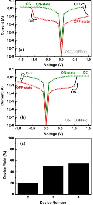
Figure 6(a) indicates that the voltage is swept to a negative voltage above a certain value (VON), and the GZO memory
devices change from the OFF state to the ON state. A compliance current of 15 mA is applied to prevent the permanent breakdown of the device. Sweeping the positive voltage over the particular value (VOFF) creates an abrupt
decrease in the current as the device switches from the ON state to the OFF state. The memory devices show successful bipolar RS behavior from both sides (ON−, OFF+ and ON+, OFF−) as shown in figures 6(a) and (b) and no unipolar RS properties are observed during the unipolar measurement process. The device yield shown in figure6(c) indicates that the devices with compact GZO nanorod thin films (devices
Nanotechnology 23 (2012) 145201 I-C Yao et al
Figure 3. (a) XRD analysis and (b) a-axis and c-axis lattice parameters of the GZO nanorod thin films changed with various Ga/Zn molar ratios in the solutions.
3 and 4) achieve higher device yields than the device with porous GZO nanorod thin films (device 2). Obviously, the devices made by using continuous and highly dense GZO nanorod thin films with a highly preferred orientation without any embedded process show an improved device yield.
Researchers have proposed various RS mechanisms to explain the RS behavior. Among the proposed models, the conducting filament formation/rupture had been employed to successfully explain the bipolar RS behavior. Figure7(a) plots the dependences of the resistance value of ON and OFF states on pattern size. The RON and ROFF seem to be insensitive to
the pattern size. Therefore, the formation/rupture of localized conducting filaments is the preferred switching mechanism of the Au/GZO nanorod thin film/ZnO/Au devices. According to the filamentary model [21, 22], the localized conducting filaments consist of defects such as oxygen vacancies are formed between the top and bottom electrodes, leading to the transition from the OFF state to the ON state. The similarity in ionic radii between Ga3+(0.62 ˚A) and Zn2+(0.74 ˚A) suggests that the gallium ion can substitute for the zinc ion. The possible defect equations of this substitution can be expressed as the following: Ga2O3 ZnO −→2Ga•Zn+3Oxo+V00Zn (1) ZnO + Oxo⇔V00Zn+2V•O+1 2O2(g) + ZnO(surface) (2)
Figure 4. (a) TEM bright-field image of device 4 (the inset is the EDS analyzed result of the point indicated) and (b) EDS element line profiles of device 4.
Figure 5. Photoluminescence spectra of the devices 1, 2, 3 and 4.
ZnO ⇔ V00Zn+2V••O +ZnO(surface) (3) Oxo⇔1 2O2(g) + V • O+e 0 (4) Oxo⇔1 2O2(g) + 2V •• O +2e 0 (5) 4
Figure 6. (a), (b) Typical bipolar RS I–V curve of device 4. (c) The yield of devices 2, 3 and 4, respectively.
where Ga•Zn denotes the gallium ion with a single positive charge in the zinc site, the V•o and V••o are the oxygen vacancies with single and double positive charges, respectively, Oxoindicates the neutral oxygen ion in the lattice site, V00Znis the zinc vacancy with a double negative charge and e0 denotes the electron with a single negative charge for compensation. According to equation (1), incorporating gallium into the ZnO nanorods generates ionic defects (V00Zn) associated with a Zn2+ site substituted by a Ga3+ ion. Furthermore, the generated defects change the equilibrium of the system. Based on equations (2)–(5) and the Le Chatelier principle [23], the system tends to shift in the direction that reduces the change in conditions (i.e. the reactions shift
towards the left-hand side as oxygen vacancies are reduced). As a result, both V00Zn and e0 suppress the formation of oxygen vacancies as the Ga/Zn molar ratios in the nanorods increase. This shows the same trend as the results of PL studies. The mobility of defects at the surface of the film is substantially higher than that in the single-crystal material (figure7(b)) [14], which suggests that V••o or V•ocan easily assemble to form conducting filaments at the surface of the single-crystalline GZO nanorod. By applying negative voltage for the devices, many positive ionic defects of V••o or V•o are expected to assemble and form conducting filaments at the interface between GZO nanorods (grain boundary). The injected electrons are simultaneously transported from the top to the bottom electrode and the device switches from the OFF state to the ON state (figure 7(c)). Applying a positive voltage on the top electrode to VOFFreleases the positive ionic
defects of V••o or V•oin the weakest region (between the GZO nanorod interface and ZnO seed layer), and the conducting filament ruptures at the interface. These result in switching to the OFF state (figure 7(d)). Applying a negative voltage to VON causes V••o or V
•
oto re-assemble, forming conducting
filaments and switching the memory state back to the ON state again (figure7(c)). The formation and rupture of conducting filaments between GZO nanorod grain boundaries and the ZnO seed layer induces bipolar RS behavior.
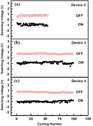
Figures 8(a)–(c) show that the VON and VOFF values
of devices 2, 3 and 4 are close, but device 2 only has 55 successful switching cycles, which is substantially less than devices 3 and 4 (with over 100 successive RS cycles each). This phenomenon demonstrates that the short circuit between the top and bottom electrodes easily occurs in porous nanorod thin films (i.e. device 2) during RS operation.
Figures 9(a)–(c) show the endurance characteristics of devices 2, 3 and 4 and their resistance ratios of the ON/OFF state, which are approximately 3, 9 and 10 times, respectively. Devices 3 and 4 with compact nanorod thin films exhibited significantly greater endurance than device 2, with porous nanorod film, and also provided sufficient memory margins to distinguish the two memory states. Devices 2–4 reach failure after their 50/100 DC cycles and the failure of the devices occurs at the OFF state. We can deduce that insufficient non-lattice oxygen ions are hard to recover from the electron-depleted oxygen vacancies under a VOFF[24].
Based on the PL spectra in figure 5 and the above defect equations, device 2 exhibits much higher oxygen vacancy concentration than devices 3 and 4, and easily forms conducting filaments along the nanorod surface. However, device 2 also has a porous nanorod film (figure2(b)), which would lead to a short circuit problem and causes a large variation in RON(44.9 ± 14.3 ) and ROFF(532.0 ± 143.7)
to decrease the resistance ratio. Devices 3 and 4 have lower concentrations of oxygen vacancies than device 2, but they exhibit highly compact nanorod thin films. This indicates that devices 3 and 4 still have sufficient oxygen vacancies existing between GZO nanorods (grain boundaries) to easily form the conducting filaments at the grain boundaries. Moreover, the compact GZO nanorod thin films provide more stable RON
and ROFF(41.4 ± 8.1 and 840.3 ± 71.8 for device 4), larger
Nanotechnology 23 (2012) 145201 I-C Yao et al
Figure 7. (a) Pattern size dependence of the resistance value in the ON and OFF states. (b)–(d) Schematic diagrams of bipolar RS mechanism of GZO nanorod film devices through the formation/rupture of conducting filaments formed between GZO nanorod side wall and ZnO seed layer.
Table 2. Comparison of RS characteristics for various ZnO nanostructure devices. Device structure Switching behavior |VON| (V) |VOFF| (V) Endurance cycles Yield (%) ON speed
(µs) OFF speed(µs) Reference Single Sb-doped ZnO
nanobelts/SiOx/p-Si
Bipolar 6 2.2 — — — — [16]
Pt/ZnO nanorods/ ITO Bipolar 0.7 0.6 120 — — — [15] Al/ZnO nanorods
embedded in PMMA/ITO
Bipolar 2 1.5 200 — — — [17]
Au/ZnO nanorod thin films/ZnO/Au (device 4)
Bipolar 0.9 0.8 100 55% 1 1 This work
Figure10 shows the electrical pulse-induced resistance change properties of device 4. The device can be successively switched between ON and OFF states by applying −8 and +6 V with a 1µs pulse width. The resistances of both ON and OFF states were measured at 0.1 V. Based on Yu and Wong’s proposed model on pulse-induced measurement [25], the pulse width decreases almost exponentially with increasing voltage pulse amplitude. In our experiment, the DC switching curve (I–V) shows low ON/OFF switching voltages (figure6(a)) with long switching time, but higher voltage is used during pulse measurement to obtain a short pulse width. After more than 60 pulse-induced switches, the resistance ratio of ON/OFF is still kept at about 1.5 times. Obviously, highly compact GZO nanorod films (devices 3 and 4) have
reversible and stable bipolar RS properties, providing the potential for NVM applications.
Table 2 shows a summary and comparison of the performance of various ZnO nanorod RS devices. Results indicate that our Au/ZnO nanorod film/ZnO/Au RS devices exhibit the same bipolar RS behavior as the other reported nanorod or nanobelt devices, but have low operational voltage, good device yield and high speed operation (1µs).
4. Conclusions
In summary, this study reports the successful fabrication of compact GZO nanorod thin film devices to avoid the short circuit between top and bottom electrodes without
Figure 8. Endurance cycle plots of VONand VOFFof devices (a) 2,
(b) 3 and (c) 4.
Figure 9. Endurance cycle plots of the ON and OFF resistances of devices (a) 2, (b) 3 and (c) 4.
any embedded process. This study also demonstrates the reversible and stable bipolar RS characteristics of the GZO nanorod thin film devices. The formation and rupture of
Figure 10. Dynamic pulse-induced resistive switching of device 4. Applying a −8 V 1µs to switch the memory state to ON state and applying a +6 V 1µs pulse to switch it back to the OFF state.
conducting filaments in the grain boundaries between GZO nanorods and the ZnO seed layer can accurately explain the switching mechanism of the GZO nanorod thin film devices. A 1D nanorod provides a straight and extensible conducting filament along the nanorod side wall, resulting in stable RS behavior. The results of this study confirm that the compact GZO nanorod thin film structure is a promising candidate for RRAM applications.
Acknowledgment
This work was supported by the National Science Council of ROC under contract no. NSC 97-2221-E-009-150-MY3.
References
[1] Lin C Y, Wu C Y, Wu C Y, Lee T C, Yang F L, Hu C and Tseng T Y 2007 IEEE Electron Device Lett.28 366 [2] Liu Q, Long S, Wang W, Zuo Q, Zhang S, Chen J and
Liu M 2009 IEEE Electron Device Lett.30 1335 [3] Lin C Y, Wu C Y, Wu C Y, Tseng T Y and Hu C 2007
J. Appl. Phys.102 094101
[4] Wang S Y, Lee D Y, Tseng T Y and Lin C Y 2009 Appl. Phys. Lett.95 112904
[5] Wu M C, Lin Y W, Jang W Y, Lin C H and Tseng T Y 2011 IEEE Electron Device Lett.32 1026
[6] Panda D, Dhar A and Ray S K 2011 IEEE Trans. Nanotechnol.11 51
[7] Kim K M, Choi B J, Jeong D S, Hwang C S and Hun S 2006 Appl. Phys. Lett.89 162912
[8] Choi B J, Choi S, Kim K M, Shin Y C, Hwang C S, Hwang S Y, Cho S S, Park S and Hong S K 2006 Appl. Phys. Lett.89 012906
[9] Sawa A, Fujii T, Kawasaki M and Tokura Y 2004 Appl. Phys. Lett.85 4073
[10] Lin M H, Wu M C, Lin C H and Tseng T Y 2010 J. Appl. Phys.107 124117
[11] Lin M H, Wu M C, Lin C H and Tseng T Y 2010 IEEE Trans. Electron Device57 1801
[12] Xu N, Liu L F, Sun X, Wang Y, Han D D, Liu X Y, Han R Q, Kang J F and Yu B 2008 Semicond. Sci. Technol.23 075019 [13] Chen M C, Chang T C, Tsai C T, Hung S Y, Chen S C,
Hu C W, Simon M S and Tsai M J 2010 Appl. Phys. Lett. 96 262110
Nanotechnology 23 (2012) 145201 I-C Yao et al [14] Panda D, Dhar A and Ray S K 2010 J. Appl. Phys.108 104513
[15] Chang W Y, Lin C A, He J H and Wu T B 2010 Appl. Phys. Lett.96 242109
[16] Yang Y, Qi J, Guo W, Zin Z and Zhang Y 2010 Appl. Phys. Lett.96 093107
[17] Tseng Z L, Kao P C, Shih M F, Huang H H, Wang J Y and Chu S Y 2010 Appl. Phys. Lett.97 212103
[18] Lee C Y, Tseng T Y, Li S Y and Lin P 2005 Nanotechnology 16 1105
[19] Vanhausden K, Warren W L, Seager C H, Tallant D R, Voigt J A and Gnade B E 1996 J. Appl. Phys.79 7983
[20] Wang Y P, Lee W I and Tseng T Y 1996 Appl. Phys. Lett. 69 1807
[21] Lin C Y, Tu B C, Lin C C, Lin C H and Tseng T Y 2006 IEEE Electron Device Lett.27 725
[22] Kim D C et al 2006 Appl. Phys. Lett.88 202102
[23] Zumdahl S S 1998 Chemical Principle 3rd edn (New York: Houghton Mifflin)
[24] Wan H J, Zhou P, Ye L and Lin Y Y 2009 J. Vac. Sci. Technol. B27 2468
[25] Yu S and Philip Wong H S 2010 IEEE Electron Device Lett. 31 1455