216 IEEE TRANSACTIONS ON NANOTECHNOLOGY, VOL. 5, NO. 3, MAY 2006
Field-Emission Triode of Low-Temperature
Synthesized ZnO Nanowires
Chia Ying Lee, Seu Yi Li, Pang Lin, and Tseung-Yuen Tseng, Fellow, IEEE
Abstract—A field-emission triode based on the low-tempera-ture (75 C) and hydrothermally synthesized single-crystalline zinc-oxide nanowires (ZnO NWs) grown on Si substrate with a silicon dioxide(SiO2) insulator was fabricated for the controllable field-emission device application. Field-emission measurement reveals that the ZnO NWs fabricated on the Si substrate exhibit a good emission property with the turn-on electric field and threshold electric field (current density of 1 mA/cm2) of 1.6 and 2.1 V m, respectively, with a field enhancement factor of 3340. The field-emission properties of the ZnO NW-based triode exhibit the controllable characteristics. The well-controlled field-emission characteristics can be divided into three parts: gate leakage region, linear region, and saturation region. Therefore, this study provides a low-temperature field-emission triode fabrication process that is compatible with the Si-based microelectronic integration, and the field-emission measurements also reveal that the emission behavior can be well controlled by adopting the triode structure.
Index Terms—Field-emission triode and device, hydrothermal method, nanowires (NWs), ZnO.
I. INTRODUCTION
C
URRENT trends in nanotechnology that include one-di-mensional (1-D) nanostructures such as nanowires (NWs), nanotubes, and nanobelts as an important class play a prominent role in the potential applications of photonic, electrooptical, and electronic devices because of their unique physical and chemical properties [1]–[4]. In particular, these high-aspect-ratio 1-D nanostructures have been extensively studied in vacuum microelectronic devices, including the field-emission display (FED), electron sources, and high-power RF amplifier for their low turn-on electric field and high elec-tron emission efficiency [3]–[5]. The main challenges of the FED are a large-area display, high productivity, high brightness, low cost, and low-power consumption. From this point of view, a triode-type FED device with a low driving voltage, high resolution, and controllable electron emission characteristics is the candidate for the next generation of FED devices.ZnO with a wide bandgap (3.4 eV) and large exciton binding energy (60 meV) has drawn much attention for the possible applications in phosphors, transparent conducting films for solar cells, ultra-violet (UV) laser devices, and flat-panel
Manuscript received March 10, 2005; revised October 17, 2005 and De-cember 19, 2005. This work was supported by the National Science Council of R.O.C. under Contract NSC 93-2216-E-009-024. The review of this paper was arranged by Associate Editor G. Ramanath.
C. Y. Lee and T.-Y. Tseng are with the Department of Electronics Engineering and Institute of Electronics, National Chiao Tung University, Hsinchu 30050, Taiwan, R.O.C. (e-mail: [email protected]; [email protected]).
S. Y. Li and P. Lin are with the Institute of Materials Science and Engineering, National Chiao Tung University, Hsinchu 30049, Taiwan, R.O.C.
Digital Object Identifier 10.1109/TNANO.2006.874049
displays [6]–[9]. Recently, the ZnO NW emitters have been reported as demonstrating good emission properties with high stability, low-threshold electric field, and high-emission current density [9], [13]. The ZnO NWs could be synthesized by various procedures [9]–[12]; however, it is hard to fabricate the NW-based FED devices because of the high synthesis temperature which limits the type of substrate materials to be used and the integration processes for a final device structure. Thus, a hydrothermal method is a suitable process for the FED fabrication because of the catalyst-free-growth, low cost, low reaction temperature, large area and uniform production, environmental friendliness, and the process compatibility to the VLSI and plastic electronics.
Although the field-emission triode based on the carbon nanotubes (CNTs) have been developed [14], [15], the device based on ZnO NWs is seldom discussed. In this paper, the hydrothermal method is adopted to fabricate the ZnO NWs in the field-emission triode device at 75 C, and the controllable field-emission characteristics were investigated.
II. EXPERIMENTS
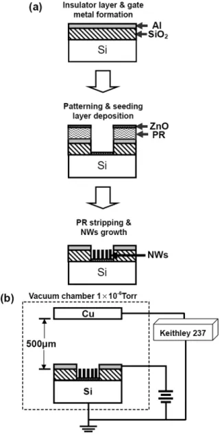
The fabrication procedure for the ZnO-based triode field-emission device is shown in Fig. 1. The details of the fabrica-tion process are summarized as follows: a gate oxide of SiO is deposited by plasma-enhanced chemical vapor deposition (PECVD), and gate electrodes of aluminum (Al) are deposited by electron beam evaporator. The cathode active region is electrically insulated from the Al gate by a 0.5- m-thick SiO layer. The emitter regions were defined by photolithog-raphy and buffer oxide etch (BOE). Then, an ultrathin ZnO seeding film was deposited on the substrate by RF sputtering (13.56 MHz) under Ar as sputtering gas at a pressure of 20 mTorr to prepare the well-aligned ZnO NWs by the hydrothermal method. Then, the photoresistance (PR) layer was stripped, and the substrate was put into an aqueous solution (Milli Q, 18.2 M cm) of zinc nitrate hexahydrate (Zn NO H O, 0.01 M) and diethylenetriamine (HMTA, C H N , 0.01 M) in a sealed vessel at 75 C for 30 min [16]. After the NWs were hydrothermally grown on the substrate, the triode device was complete. The surface morphologies were confirmed by field-emission scanning electron microscopy (FE-SEM, Hitachi S-4700I, Japan). The test scheme cor-responding to the field-emission properties is illustrated in Fig. 1(b). A Keithley 237 current–voltage analyzer was used for measuring the field-emission characteristics at a base pressure of 1 torr at room temperature, and a power supply was adopted for the control of the gate bias . A copper electrode probe that acts as an anode with the tip diameter of 500 m
LEE et al.: FIELD-EMISSION TRIODE OF LOW-TEMPERATURE SYNTHESIZED ZnO NANOWIRES 217
Fig. 1. Schematic description of fabrication processes of field-emission triode.
was placed at a distance of 500 m from the tips of the NWs. The distance between cathode and anode was adjusted by a precision vernier with an accuracy of m.
III. RESULTS ANDDISCUSSION
The SEM image of the fabricated ZnO-based triode structure is shown in the inset of Fig. 2(a), indicating that the cathode ac-tive region is 100 100 m , and the distance between the two active regions is 500 m. The gate region here is 2 2 mm . The rectangular islands of ZnO NWs are successfully and selectively grown on the ZnO seeding areas, but no NWs are grown on the gate region. Fig. 2(a) is the enlarged image of the triode device, in which well-aligned ZnO NWs with a diameter of 50 nm and a number density of 3.4 cm are uniformly grown on the ZnO seeding layer. The cross-sectional SEM image of ZnO NWs on the substrate is shown in Fig. 2(b), indicating that the ZnO NWs were directly grown on the substrate with an average length of 500 nm. The polycrystalline ZnO seeding film with the distinct orientation results in the nonvertical random distri-bution of ZnO NWs.
Fig. 2. (a) FE SEM microphotographs of the triode near the gate edge. The inset is the 42 5 array triode with the ZnO NW islands grown inside gate holes. (b) Cross-sectional FE SEM image of ZnO NWs on the substrate.
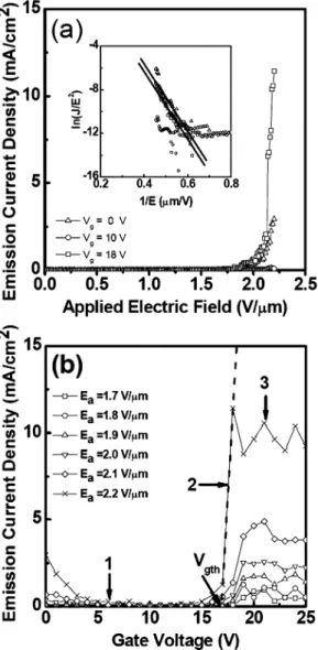
The relationship between emission current density and applied electric field of the ZnO NW-based triode for different gate bias is shown in Fig. 3(a). The threshold electric field (at a current density of 1.0 mA/cm ) is 2.1 V m under the zero gate bias. As increases to 10 V, is depressed to 36 A/cm under the of 2.1 V m. While increases to 18 V, slightly decreases to 2.0 V m, but abruptly increases to 12 mA/cm under of 2.2 V m. The corresponding Fowler–Norheim (F-N) plots versus are depicted in the inset of Fig. 3(a), and the field-enhancement factor can be calculated from the slope of the F-N plot by adopting the work function of ZnO (5.37 eV) [9]. As shown in the figure, the F-N plot under a of 10 V is deviated from the F-N fitting and that under of 0 and 18 V are obeying the fitting with the same slope. The calculated value of a ZnO NW-based triode under a of 0 V is 3340. The relationships between , , and values are unusual, and they will be discussed next.
The characteristic plots of versus at various valuesof are shown in Fig. 3(b), indicating that a controllable behavior could be divided into three parts: gate leakage region (region 1), linear region (region 2), and saturation region (region 3). After applied electric field, the electron can be emitted from ZnO NW emitters under of 0 V. decreases with an increase in in region 1. With an increase of from 0 V, the electric field gradient near the ZnO NW emitters will increase due to the short emitter-gate spacing, but some emitted electrons might be trapped by the gate, which results in a lower and leads to the deviation from the F-N fitting at a of 10 V [see Fig. 3(a)]. As is continuously increased up to 14 V, abruptly increases at the linear region (region 2). The linear intercept on the -axis is the linear region threshold voltage . It is believed that, at region 2, the induced electric field gradient is large enough to accelerate the electrons; consequently, the emitting electrons gain momentum while passing through the gate without being trapped. It is well known that the value depends only on the
218 IEEE TRANSACTIONS ON NANOTECHNOLOGY, VOL. 5, NO. 3, MAY 2006
Fig. 3. (a) Field-emission current density versus applied electric field curves under the gate voltages of 0, 10, and 18 V, respectively. The inset is the corresponding F-N plots. (b) Field-emission current density versus gate voltage (J 0 V ) curves under the various applied electric field.
geometry, structure, tip size, and number of emitters on the sub-strate; thus, the value should be constant under various gate voltages. However, there is a large deviation from the F-N fitting at of 10 V, as indicated in the inset of Fig. 3(a). It is suggested that the gate trapping is the main mechanism; the electrons are emitted under the F-N mechanism but are trapped by the gate, which results in the low current density and the large deviation from the F-N fitting under a of 10 V. The high emission cur-rent of the triode operated in region 3 is assumed to be due to the short gate-tip spacing, small gate aperture, and high aspect ratio of the ZnO NWs. Moreover, the fact that the saturates (region 3) as the is larger than 18 V is due to the space-charge effect of the semiconductor emitters [17].
The field-emission characteristics also could be observed in the variation of small-signal transconductance . Fig. 4 de-picts the relationships between and of the ZnO NW-based field-emission triode. The is defined as
Fig. 4. Relation of transconductance versus gate voltage of the field-emission triode.
It should be noted that is nearly zero below because is very small in the gate leakage region. It goes through a maximum at the point of inflection of linear region to the satu-ration region in the - curve, and then decreases. The ZnO NW-based triode exhibits a high of 2.2 S under the ap-plied electric field of 2.2 V m and a low operating gate bias of 17 V, which is the optimized operation of the field emission triode. Then decreasing values of in the saturation region are due to the space-charge effect.
IV. CONCLUSION
A field-emission triode based on low-temperature hydrother-mally grown ZnO NWs was successfully fabricated. The ZnO NW-based triode emitter was design with a 100 100 m cathode active region. This device exhibits gate-controllable be-havior and emits electrons at a value of 14 V and up to 12 mA/cm under of 18 V and of 2.2 V m. The triode also displays a high of 2.2 S at a low operating of 2.2 V m and of 17 V. Thus, this field-emission triode with controllable transistor characteristics may be appropriate for field-emission display applications.
REFERENCES
[1] X. Hu and C. T. Chan, “Photonic crystals with silver nanowires as a near-infrared superlens,” Appl. Phys. Lett., vol. 85, pp. 1520–1522, 2004. [2] Y. J. Chen, Q. H. Li, Y. X. Liang, T. H. Wang, Q. Zhao, and D. P. Yu,
“Field emission from long SnO nanobelt arrays,” Appl. Phys. Lett., vol. 85, pp. 5682–5684, 2004.
[3] S. Hofmann, C. Ducati, B. Kleinsorge, and J. Pobertson, “Direct growth of aligned carbon nanotube field emitter rays onto plastic substrates,”
Appl. Phys. Lett., vol. 83, pp. 4661–4663, 2003.
[4] O. J. Lee and K. H. Lee, “Fabrication of flexible field emitter arrays of carbon nanotubes using self-assembly monolayers,” Appl. Phys. Lett., vol. 82, pp. 3770–3772, 2002.
[5] V. V. Zhinov, E. I. Givarfizov, and P. S. Plekhanov, “Field emission from silicon spikes with diamond coatings,” J. Vac. Sci. Technol. B, vol. 13, pp. 418–421, 1995.
[6] C. X. Xu, X. W. Sun, C. Yuen, B. J. Chen, S. F. Yu, and Z. L. Dong, “Ul-traviolet amplified spontaneous emission from self-organized network of zinc oxide nanofibers,” Appl. Phys. Lett., vol. 86, pp. 011118–011120, 2005.
LEE et al.: FIELD-EMISSION TRIODE OF LOW-TEMPERATURE SYNTHESIZED ZnO NANOWIRES 219
[7] S. Fujihara, A. Suzuki, and T. Kimura, “Ga-doping effects on electrical and luminescent properties of ZnO:(La,Eu)OF red phosphor thin films,”
J. Appl. Phys., vol. 94, pp. 2411–2416, 2003.
[8] T. Miyata, Y. Minamino, S. Ida, and T. Minami, “Highly transparent and conductive ZnO:Al thin films prepared by vacuum arc plasma evapora-tion,” J. Vac. Sci. Technol. A, vol. 22, pp. 1711–1715, 2004.
[9] S. Y. Li, P. Lin, C. Y. Lee, and T. Y. Tseng, “Field emission and-photofluorescent characteristics of zinc oxide nanowires synthesized by a metal catalyzed vapor-liquid-solid process,” J. Appl. Phys., vol. 95, pp. 3711–3716, 2004.
[10] B. P. Zhang, K. Wakatsuki, N. T. Binh, Y. Segawa, and N. Usami, “Low-temperature growth of ZnO nanostructure networks,” J. Appl. Phys., vol. 96, pp. 340–343, 2004.
[11] J. J. Wu and S. C. Liu, “Low-temperature growth of well-aligned ZnO nanorods by chemical vapor deposition,” Adv. Mater., vol. 14, pp. 215–218, 2002.
[12] L. Vayssieres, K. Keis, A. Hagfeldt, and S. Lindquist, “Three-dimen-sional array of highly oriented crystalline ZnO microtubes,” Chem.
Mater., vol. 13, pp. 4395–4398, 2001.
[13] Y. B. Li, Y. Bando, and D. Golgerg, “ZnO nanoneedles with tip surface perturbations: Excellent field emitters,” Appl. Phys. Lett., vol. 84, pp. 3603–3605, 2004.
[14] C. L. Tsai, C. F. Chen, and C. L. Lin, “Field emission from well-aligned carbon nanotips grown in a gated device structure,” Appl. Phys. Lett., vol. 80, pp. 1821–1822, 2002.
[15] I. T. Han, H. J. Kim, Y. J. Park, N. Lee, J. E. Jang, J. W. Kim, J. E. Jung, and J. M. Kim, “Fabrication and characterization of gated field emitter arrays with self-aligned carbon nanotubes grown by chemical vapor deposition,” Appl. Phys. Lett., vol. 81, pp. 2070–2072, 2002. [16] C. Y. Lee, S. Y. Li, P. Lin, and T. Y. Tseng, “ZnO nanowires
hydrother-mally grown on PET polymer substrates and their characteristics,” J.
Nanosci. Nanotechnol., vol. 5, pp. 1088–1094, 2005.
[17] C. W. Lu and C. L. Lee, “Direct current circuit simulation model for a field emission triode,” J. Vac. Sci. Technol. B, vol. 16, pp. 2876–2880, 1998.
Chia Ying Lee received the B.S. degree in chemical
engineering from National Taiwan University, Taipei, Taiwan, R.O.C., in 2001, the M.S. degree from the In-stitute of Electronics, National Chiao Tung Univer-sity, Hsinchu, Taiwan, R.O.C., in 2003, and is cur-rently working toward the Ph.D. degree at the Insti-tute of Electronics, National Chiao Tung University. Her research interests are nanomaterials, material analysis, field-emission ability, and nano-devices.
Seu Yi Li received the B.S. degree in electrical
engineering from the University of Tatung, Taipei, Taiwan, R.O.C., in 1996, the M.S. degree in electrical engineering from the University of Tatung, Taipei, Taiwan, R.O.C., in 1998, and the Ph.D. degree in material science and engineering from the National Chiao Tung University, Hsinchu, Taiwan, R.O.C., in 2005.
He is now a Principal Engineer with the Depart-ment of DevelopDepart-ment for Manufacturing, Advanced Module Technology Division, Taiwan Semicon-ductor Manufacturing Division, Hsinchu, Taiwan, R.O.C. His research interests include back-end-of-line interconnect development and nanotechnology.
Pang Lin, photograph and biography not available at the time of publication.
Tseung-Yuen Tseng (M’94–SM’94–F’02) received
the Ph.D. degree in electroceramics from the School of Materials Engineering, Purdue University, West Lafayette, IN, in 1982.
After working at the University of Florida, Gainesville, he became a faculty member with the National Chiao-Tung University, Hsinchu, Taiwan, R.O.C., in 1983, then the Director of the Institute of Electronics, and he is now a Chair Professor with the Department of Electronics Engineering and the Institute of Electronics and a Chair Professor with the Department of Materials and Mineral Resources Engineering and Dean of the College of Engineering of National Taipei University of Technology, Taipei, Taiwan, R.O.C. He established the Electronic Materials Research Laboratory and High Temperature Superconductor Thin Film Laboratory at the Institute. His current research interests are in electronic ceramics, nanomaterials and nanodevices, passive components, high-k gate dielectrics, ferroelectric thin films and devices, and electronic ceramic thin films and devices. He has published more than 210 journal papers and 70 conference papers and holds several patents.
Dr. Tseng is a reviewer for a number of scientific journals, a member of ed-itorial board of the Journal of Nanoscience & Nanotechnology, and a member of the board of Asia Ferroelectrics Association and National Science Council Distinguished Research Fellow. He has received the Distinguished Research Awards of the National Science Council (1995–2000), the Distinguished Elec-trical Engineering Professor Award of the Chinese ElecElec-trical Engineering So-ciety (2000), the Lou Cbin-Tui Distinguished Honor Award (2002), the Sun Yat-Sen Academic Award (2003), TECO Technical Award (2004), and the IEEE CPMT “Exceptional Technical Achievement Award” (2005) for his contribu-tions to the applied technology and basic science of electronic ceramics.