Thin Solid Films 260 (1995) 47 53
The effect of anodizing temperature on anodic oxide formed
on pure Al thin films
Re-Long Chid’, Peng-Heng Char@, Chih-Hang Tungb
Received 2 June 1994; accepted 6 December I994
Abstract
The structure and properties of anodic Al,O, films formed at different anodizing temperatures from thin Al films deposited by magnetron sputtering on oxidized Si wafers have been studied by transmission electron microscopy. secondary ion mass spectrometry, and electrical measurements. The anodic oxide films formed at 8 “C and 25 “C are amorphous with excellent dielectic properties, leakage current lower than 500 nA at 7.5 MV cm- ’ and no breakdown up to 7.5 MV cm ‘. Partially crystalline I”-A&O, is grown at the upper half of the 58 “C oxide film. This film exhibits much inferior dielectric properties than the lower temperature films. Carbon is incorporated into the top portion of the oxide films from the electrolyte during anodizing and it has little effect on the crystalline oxide formation. Oxygen penetrates into the underlying Al layer during anodizing. The penetration increases with increasing anodizing temperature.
Kq~or~Lss: Aluminium oxide; Anodic oxidation; Dielectric properties: Transmission electron microscopy
1. Introduction
7 he low resistivity and the well-established process technology of Al make it an attractive candidate for metallization in large size, high resolution, thin film transistors (TFT) liquid crystal display (LCD) applica- tion [l]. However, the propensity for hillock formation in thin film Al on Si substrates during heat processing has, until recently, prevented its application in TFT; LCD [2]. Hillocks generally form on Al films in order to relieve planar compressive stresses introduced either during deposition or subsequently by substrate-induced diherential thermal expansion strains [3]. Recently, it wa$ reported [l] that anodic aluminum oxide films can be used as a protective layer against hillock formation. Thin film transistors with Al gates and an anodic Al:O, + Si, N, double layer gate insulator have been successfully applied to the 10.4 in diagonal multicolor LCD display panel [l].
‘Two types of anodic aluminum oxide film can be for-med on Al depending on the electrolyte used in
0040-6090 95, SO9.50 (” 1995 ~ Elsevier Science S.A. All rights reserved s.sn/ 0040.hO9,0(94)0649 I -I
anodization [4]. These are the thin, impervious barrier type and thick porous type films. For integrated circuit (IC) applications, the use of anodic A120, has been limited to the barrier films. Depending on the anodizing conditions, the anodic oxide film may be either amor- phous, crystalline, or a mixture of both [5-71. The degree of crystallinity of the anodic oxide generally increases with decreasing current density and increasing voltage [6, 71. Crystalline films have a higher capaci- tance because of a larger dielectric constant [7], but exhibit an electrical instability [B] which is related to the presence of voids [9] and,/or to the trapped oxygen [IO]. For integrated circuit applications, the characteristics of the anodic aluminum oxide film are very important. In a previous paper we have studied the anodic oxide film formed on pre-annealed Al thin films containing 1% Si and 0.5% Cu [ll]. In this paper the anodic oxide formed on pure Al film without any pre-anneal is investigated. The effects of anodizing temperature on the structure, chemistry, and dielectric properties of the oxide films are examined in detail.
48 R.-L. Chiu ri al. I Thin Solid Films 260 (1995) 47-53
2. Experiment 351
The substrates for this study were 4 in diameter, p-type, (loo), Si wafers. To simulate a typical glass
substrate used for LCD, a 550 nm thermal oxide was first grown on the substrate and a 600 nm thick borophosphosilicate glass (BPSG) was subsequently de- posited by chemical vapor deposition at 720 “C. A 300 nm thick pure Al film was then deposited by d.c. magnetron sputtering on top of the BPSG layer. A&O, was grown by anodizing the samples in AGW elec- trolyte [12], which is a mixture of 3% aqueous solution of tartaric acid and propylene glycol at a volume ratio of 2 to 8. The electrolyte temperature was kept at either 8, 25, or 58 “C in a constant-temperature water bath during anodizing. Stainless steel was used as the coun- ter-electrode, and typically about 90% of the wafer was immersed in the electrolyte while the exposed one tenth was connected to the anode through a Cu clamp. A programmable Keithley 237 Current/Voltage Source- Measure Unit interfaced to a PC capable to sourcing and measuring voltage or current simultaneously was used as the power supply and the data logger. Constant current mode (current density = 0.4 mA cmp2) was em- ployed initially until the voltage reached 100 V; the anodizing was then automatically switched to constant- voltage mode. The total time of anodization was kept to 40 min, constant for each run. A 400 nm thick Al film was sputtered on the anodized wafers and metal/ insulator/metal (MIM) capacitors were fabricated for the subsequent current-voltage (I- V) and capaci- tance-voltage (C- V) characterization using the Al layer as the top electrode. The MIM capacitor elec- trodes are 200 x 200 urn squares. The I- V measure- ments were carried out with a HP 4145B Semiconductor Parameter Analyzer and the high-fre- quency (1 MHz) capacitance measurement was per- formed using a Keithley 82 C- V system. The structures of the oxide films were studied by transmission electron microscopy (TEM). Both cross-sectional and planar TEM samples were prepared by ion milling in the usual fashion [13] and examined with a Philips CM20 micro- scope operating at 160 kV. Depth profiles of the chemi- cal composition of the films were determined by secondary ion mass spectrometry (SIMS) with a Cameca IMS-4F instrument using Cs+ primary beam of 14.5 keV impact energy of 50 nA current.
30 25
5
0
Fig. 1, Variation of current with time during anodizing.
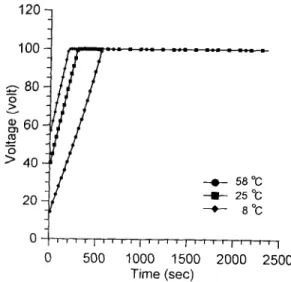
reached 100 V). Apparently, the lower the electrolyte temperature the faster the anodizing voltage reaches 100 V. The 58 “C curve in Fig. 1 shows a peak at 2000 s, which is probably caused by a sporadic, local- ized dielectric breakdown during anodizing. The anodic current is eventually decreased to about 0.52 mA (0.007 mA cm--*), independent of temperature.
In Fig. 2, the initial rise of the curves corresponds to the stage where the anodization was conducted in con- stant current mode. The fact that the lower the temper- ature the higher the voltage in Fig. 2 during this initial period indicates that higher voltage is required for the lower-temperature electrolyte to reach the same current density level. Since this difference is observed from the very beginning of the anodizing when the conditions of the growth native oxide are the same for the three samples, it may be attributed to the decreased ionic
120 7
3. Results and discussion -e- 58°C
20 -I)- 25°C
t- 8°C The variations of current and voltage with time
during anodizing at different temperatures are shown in Fig. 1 and Fig. 2 respectively. In Fig. 1, the sudden drop of the anodic current from 30 mA signifies the onset of constant voltage mode (i.e. the voltage has
00
0 500 1000 1500 2000 2500 Time (set)
Fig. 2. Variation of voltage with time during anodizing.
-o- 8°C
t 25%
-a- 58 “c
500 1000 1500 2000 2500 Time (set)
mobility of the electrolyte at lower temperatures so that higher electric field strength is needed for a given current density. The rate of increase in voltage (defined as voltage growth rate) during the constant current period, which is the slope of the slanted lines in Fig. 2, varies slightly with the anodizing temperature, being 0.21 V s ’ at 8°C and 25°C but 0.16 V SK’ at 58°C. This variation in presumably due to the difference in the microstructure of the anodic oxide films formed at different temperatures.
Fig. 3 shows cross-sectional TEM (XTEM) micro- graphs of the A&O, films anodized at 8, 25, and 58 “C respectively. The two lower-temperature oxide films are very similar: both are amorphous and practically pin- hole-free (see Fig. 3(a) and (b)). The 58 “C oxide film shoun in Fig. 3(c), however, is composed of two layers: an impervious amorphous layer at the bottom and a void-impregnated crystalline layer on the top. Fig. 4 shows the 58 “C films at a higher magnification, which shows clearly that the top layer is completely crys- talline, and numerous patches of amorphous A&O, can be observed in it. In some locations, an example of which is marked by the arrow in Fig. 4, the Al,O, is even completely amorphous throughout the entire layer. The voids associated with the crystalline oxide seem to concentrate near but not at the bottom of the crystalline region, and they appear as cracks in the film.
These cracks may be responsible for the localized breakdown observed in Fig. 1.
The nature of the crystalline phase in the 58 “C oxide film is better investigated with planar TEM specimens because a larger area is available for examination. Fig. 5(a) is a plane view bright-field image of the upper crystalline layer, and the corresponding dark-field im- age of the same area is shown in Fig. 5(b). Dispersed
Fig. 4. Cross-sectional TEM images showing the enlargement micro- structure of the Al,O, films anodized at 58 “C.
Fig. 5. Planar TEM images of the Al,O, film shown in Fig. 2(c): (a) is a bright field image and (b) is the corresponding dark field image.
50 R.-L. Chiu et d. i Thin Solid Films 260 (1995) 47 53
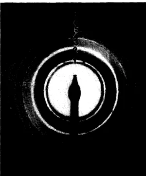
Fig. 6. Electron ditfraction pattern taken from the crystalline AlJO, layer in a 58 “C oxide film. The rings can all be ascribed to the ;I’-AI,O, phase as indexed in Table I.
small crystallites and amorphous patches are clearly discernible in these micrographs.
Diffraction patterns taken from this region (Fig. 6) were indexed using the substrate Si as the internal standard. The d-spacings corresponding to the rings in Fig. 6 are listed in the first column of Table 1 together with the description of their relative intensities in the second column. It is generally believed that anodic crystalline alumina is usually the I)‘-phase alumina grown from nuclei originally existing in the form of y-phase alumina [14]. Table 1 also gives the diffraction data for the y-Al,O, [I 51, “/‘-A&O, [16] and pure Al [17]. It turns out that the d-spacings of many lattice planes in the three reference phases are very similar. For example, the d-spacing for the (200) of ;I-Al,O,, the (400) of Y’-A&O, and the (200) of Al is 1.980, 1.977, and 2.024 A respectively. This minor difference is well within the experimental error in the electron diffraction work, making the identification of the rings in Fig. 6 somewhat ambiguous. Careful comparison of the ex- perimental data with three reference structures shows, however, that the ring pattern in Fig. 6 is most likely due to the y’-Al,O, phase for the following reasons.
(1) The experimental d-spacings and the correspond- ing intensities agree most favorably with the y’-Al,O, results of Stirland and Bicknell [16].
(2) Although the missing four reflections, (11 l), (220) (311) and (511), of the Y-A&O, phase in the experimental data are insufficient to rule out the pres- ence of y-A&O,, the observed spacing of 1.205 A defin- itely cannot be attributed to the ;‘-AI,O, phase. These
two facts combined strongly suggest that the crystalline oxide is unlikely to be y-alumina.
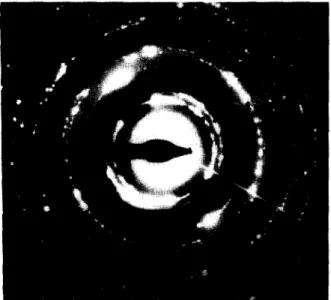
(3) The observed d-spacings can also be matched reasonably well with the &spacings of pure Al, so the question may be raised as to whether the crystalline material is actually the remnant Al layer on the amor- phous alumina. But we believe this is not the case, because the diffraction pattern shown in Fig. 6 is totally different from the pattern taken from the Al layer in the same specimen (see Fig. 7). It should be pointed out that the diffraction pattern in Fig. 7 is in excellent agreement with the Al standard pattern, both in the d-spacings as well as in the relative intensities.
The mixed nature of the top crystalline layer is also confirmed by high-resolution TEM (HRTEM). Fig. 8 shows a HRTEM micrograph of the top layer in a 58 “C oxide film, which reveals both the small II’-Al,O, crystallites and the patches of amorphous oxide. The size of the 1”-Al,O, crystallites is about 50 nm or less. It is well known that the growth of anodic A&O3 films is due to the mixed transport of both cations and anions, and that the growth occurs at both the Al/Al,O, inter- face and the Al? 0,jelectrolyte interface [18, 191. Crys- talline anodic Al,O, layers are known to form on Al metal pre-annealed in an oxidizing atmosphere at a temperature higher than 450 “C. In such a case the crystalline layer is always formed near the center of an otherwise impervious amorphous layer. It has been convincingly demonstrated that the pre-annealing treat- ment causes crystalline y-A&O, nuclei to form on the surface of the Al metal, and subsequent growth of the anodic AllO, film at the two interfaces buries these nuclei roughly in the center of an amorphous Al,O, layer. The further growth of the crystalline nuclei is induced when a critical field strength is reached at a latter part of the anodization, and the growth proceeds by the crystallization of the nearby existing amorphous ALOt materials. Eventually a continuous crystalline A&O, layer would be formed in the center of an amorphous oxide film.
To prevent the formation of crystalline y-A&O, nu- clei on the Al films in the present study, we have purposely avoided the pre-anneal treatment and have, therefore, successfully prevented the crystalline Al,O, layer formation at the two lower temperatures. (It should be pointed out that in a parallel study [l I],
crystalline oxide film was indeed formed in a sister sample which had gone through exactly the same treat- ment as the 25 “C oxide film of the present study except that the sample was pre-annealed at 410 “C for 30 min in air.) Although the crystalline Al,O, layer still forms in the 58 “C oxide film, it forms at the top of the oxide layer instead of being interposed in the center as in the pre-annealed samples. Being at the top of the anodic oxide layer indicates that they are not grown from the existing 1’-Al,O, nuclei which might have been present
Comparison 01‘ diti’raction spectra of Al, ;,‘- and ;s-alumina
ExperImental data from ;,‘-alumina standard ;,-alumina standard Aluminum standard
Fig, 6 (Stirland and Bicknell) [I61 (JCPDS 10-425) [I51 (JCPDS 4-0787) [I71
Ring f L, (A) Intensit) (hhl) Li (A) lntensitl (/I/,/) 4,,,, (84) Intensity (IrhO 4,i, (A) Intensity
(III) 2.287 VVF (NO) I.980 s (III) 4.56 (220) 2.80 (31 I) 2.39 (232) 2.7X (400) I .Yl7 (511) I .5X (440) I .?Y5 MS M s MS VS M VS I I.Y58 s 2 I.417 VS (220) 1.399 VS 3 I.205 VF (31 I) I.193 VF
4 I.146 M (222) I.143 M (444) I.140 M
5 I .o F (400) 0.988 F (7.31) 1.027 F
(800) 0.9x’) F
6 0.895 M (420) 0.885 M (844) 0.884 F
I O.XIX M (422) 0.805 S (844) 0.806 M
VS. \ery strong: S, strong; M. medium: F. faint; VF, very faint: VVF. very very faint
(Ill, (2OOl (270) (111) (2221 (400) 031) (4’0) (42’) 2.33x 1.024 I .Ji I I.721 l.l6Y l.l)12 0.92’) 0.906 0.827 vs s M M F V F I F
on ihe surface of the as-deposited Al films. Since the top surface of the oxide layer is a place where new oxide continuously forms, the crystalline oxide layer formed there must be a growth product rather than a transformation product formed by the crystallization of the existing amorphous AllO, layer. The fact that crystalline A&O, forms only in the 58 “C film but not in the 8 “C at 25 “C films shows that it is due. primarily, to a thermal effect. It is likely that the heat generated during anodizing cannot be easily removed from the upper oxide layer adjacent to the hot electrolyte, mak- ing the temperature there so high which, coupled with the applied electric field, favors the crystalline Al,O,
formation. The bottom layer of the oxide film, on the other hand, is in contact with the Al layer which, in our experimental set-up, is exposed to the ambient air out- side the electrolyte. Since Al is an excellent conductor, the heat generated at the bottom of the oxide layer can be easily dissipated, so the temperature at the A1:‘A120, interface remains low enough to favor the amorphous Al,O, growth.
Anodically formed crystalline Al,O, films are often associated with voids and pores. and this observation has been reported by numerous investigators [5, 6, 141. Three models have been proposed for their origin: (I) voids are produced by the volume contraction associ-
Fig. 7. Electron difiraction pattern taken from the polycrystalline Al film. Reflecting planes corresponding to the numbered rings are: I-(: I I ). 2-(2(N)). 3-(2X). 4-(31 I), S-(222). 6-(400). 7-(331). 8-(4X)). Y-(422).
Fig. 8. High resolution TEM image of the crystalline AIZO, layer. Both ;‘-AI,O; crystallites and amorphous patches are discernible.
52 Table 2
R.-L. Chiu et al. / Thin Solid Films 260 (1995) 47-53
Dielectric properties of the anodic films” Anodic
temp. (“C)
Capacitance (pf) Leakage current (nA)
Mean s.d.b Mean s.d.b Oxide thickness (nm) Dielectric constant Breakdown field (MV cm-‘) 8 24.22 0.876 299.6 162.3 125 8.5 25 24.46 0.594 483.2 278.0 135 9.2 58 25.56 I.656 1321.3 95.2 125 9.0 No breakdown No breakdown 7.9
“MIM capacitor electrode area = 200 x 200 pm’ %tandard deviation.
ated with the amorphous-to-crystalline transition [5]; (2) voids are formed by the trapped oxygen atoms near the crystalline particle during anodizing [6]; and (3) voids are formed by vacancy condensation [20]. The presence of voids and pores is detrimental to the dielec- tric properties of the oxide films. Fig. 9 is a Frenkel- Poole plot of the leakage current per electric field versus the square root of the electric field for the three films anodized at 8 “C, 25 “C and 58 “C. The leakage cur- rents of the A&O, films were found to increase with temperature, and were mainly dominated by Frenkel- Poole emission, which is due to field-enhanced thermal excitation of trapped electrons into the conduction band [21]. Table 2 summarizes the dielectric properties of the oxide films. Here, the leakage current is defined as the current at 100 V and the breakdown field is the electric field corresponding to the current of 1 PA. The oxide thickness was measured directly on XTEM mi- crographs, and the dielectric constant was calculated from the capacitance and thickness data. It is evident from Table 2 that the dielectric properties of the 8 “C and 25 “C films are comparable while the 58 “C film shows a slightly larger capacitance, comparable dielec- tric constant, and much larger leakage current and lower breakdown field. The dielectric constant of our
IE-2 1 lE-3 - lE-4- >^ 6 lE-5 - a $lE-6- g lE-7- IE-9 1, 0 J&I 03&j 3
Fig. 9. CurrentPvoltage characteristics of the anodic oxide films formed at three different temperatures.
anodic oxide films is in the range of 8.5-9.2, which is consistent with the published data of 8.2-10.2 [22]. The larger leakage current observed in the 58 “C film is possibly due to the voids and the crystalline grain boundary in the oxide layer. The dielectric properties of our anodic oxide films compare favorably with those of Al,O, films prepared by other methods, such as reactive electron beam evaporation (dielectric constant c= 7.6-7.8, breakdown field E, = 1 MV cm-‘) [23], chemical vapor deposition (E = 7.1-9.2,
Es = 7.4 MV cm- ‘) [24], and oxygen plasma deposition
(E= 7-8, E, = 4-8 MV cm-‘) [25].
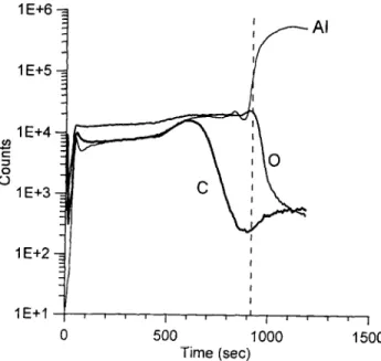
The effect of anodizing temperature on the film chemistry can be evaluated by SIMS analysis. Figs. 10 and 11 show respectively the composition profiles of the films formed at 8 “C and 58 “C. The Al,O,/Al interface is marked roughly by the vertical dashed line in each figure. The most striking feature here is the carbon pick-up in the oxide film, which is shown by the much higher (about 1.5 order of magnitude) carbon intensity in the oxide film than in the underlying Al film. The carbon is apparently coming from the electrolyte, which consists of tartaric acid (HO, C(CHOH), COOH) and
1 E+6 1 E+5 4 1 E+4 d 5 0” 1 E+3 500 1000 Time (set)
R.-L. C’hiu ci al. I Thin Solid Films 260 (1995) 47 5.? 53 lE+Q 1 E+5 i lE+27 I I I I I lE+l I I I I, I I I I, I 1 I I I 0 500 1000 1500 Time (set)
Fig. I I SIMS profile of the AlzO, films anodized at 58 “C.
propylene glycol (CH,-CHOHPCH,OH). Note that in both figures the carbon pick-up does not extend all the way to the Al,O,/Al interface, similar to phosphorus pick-up with phosphate-based electrolyte [18, 261 or the boron pick-up with borate-based electrolyte [18] re- ported in the literature. Carbon incorporation from the electrolyte is evidently not affecting the structure of the oxide film because both films contain carbon and yet one is amorphous but the other is mixed (amor- phous + crystalline) type.
Another interesting observation from the SIMS profiles is the oxygen tails in the Al layer. Comparing the oxygen profile with the AI profile in Figs. 10 and 11, it is clear that the oxygen has penetrated deeper into the underlying Al layer in the 58 “C film than in the 8 “C film. This is probably due to the increased oxygen transport rate with increasing anodizing temperature.
4. Conclusions
(1) The anodic oxide films formed at 8 “C and 25 “C are completely amorphous and pinhole free. The dielectric properties of the low-temperature films are good, with leakage current lower than 500 nA at 7.5 MV cm-‘, and no breakdown is detected up to 7.5 MV cm ‘.
(2) Crystalline ;“-A&O, is formed at the upper half of the oxide layer in the 58 “C film. This film exhibits inferior dielectric properties compared with the low- temperature, amorphous oxide films.
(3) Carbon is incorporated into the top portion of the oxide films from the electrolyte during anodizing, and it has little effect on the crystalline oxide forma- tion.
(4) Oxygen penetrates into the underlying Al layer during anodizing. The penetration increases with in- creasing anodizing temperature.
Acknowledgment
This work was partially supported by the National Science Council of Republic of China under contract number: NSC 83-0404-E-009-098.
References
[I] H. Yamamoto. H. Matsumaru. K. Shirahashi. M. Nakatani, A. Sasano, N. Konishi. K. Tsutsui and T. Tsukada, l990 In/. ,!&c.trorz Drric,r Mrg.. Tech. Dig., San Frrmc~i.~so. C‘A, 1990. IEEE. New York, 1990, p. 851.
[2] T. Sunata. T. Yukawa, K. Miyake, Y. Matsushita, Y. Mu- rakami, Y. Ugai. J. Tamamura and S. Aoki. IEEE Truns. Ekrron. Drtkrs, ED-33 (1986) I2 12.
[3] C. Y. Chang and R. W. Vook. Thin Solid Films. 228 (1993) 205. [4] V. F. Henley. Anodic Ouidtrrion of Aluminum & Its Allops,
Pergamon Press, Oxford. 1982.
[5] K. Kobayashi and K. Shimizu. in R. S. Alwitt (ed.). Aluminum Swfuce Trratmrnf Twhnok+_y. The Electrochemical Society. Pennington, NJ, 1986. p. 380.
[6] C. Crevecoeurs and H. J. de Wit. J. Ek.c./roc~/wm. Sot,.. 1.14 (1987) 808.
[7] C. T. Chen and G. A. Hutchins. J. E/ec,troc,/rem. Sot,., 1.12 (1985) 1567.
[8] R. S. Alwitt and C. K. Dyer, Ektrochim. Ac,/tr, 2.3 (1978) 355. [9] R. S. Alwitt, C. K. Dyer and B. Noble. J. Ehrroc~hm~. SW..
129(1982) 711.
[IO] W. J. Bernard and P. G. Russell, J. Elrc~rroc~hn. Sot.. /27( 1980) 1256.
[I I] R. L. Chiu. P. H. Chang and C. H. Tung. J. Elrctrochrm. Sock.,
142 (1995) 525.
[12] H. Hasegawa and H. L. Hartnagel. J. Ekc~trochem. SOCK., 12.3
(1976) 713.
[I31 P. H. Chang, H. Y. Liu, J. A. Keenan and J. M. Anthony. J. Appl. Phys., 62 (1987) 2485.
[I41 K. Kobayashi and K. Shimizu, J. E/w/roc~hem. Sot.. 13.5 (1988) 908.
[ 15) Powder DQhcfion File # 10-425, International Center for Ditfraction Data, 1601 Part Lane, Swarthmore. PA 19081. USA. [I61 D. J. Stirland and R. W. Bicknell, J. E/rc~trt~chm~. Sock., 106
(1959) 484.
[I 71 Pore&r D$jracrion File # 4-0787. International Center for Diffraction Data, 1601 Part Lane, Swarthmore, PA 19081, USA. [18] G. E. Thompson and G. C. Wood, in J. C. Scully (ed.), Trealisr
on Murerials Scirncr and Trcl~nolo~~~, Vol. 23, Academic Press. London, 1983, p. 205.
[I91 J. P. Pringle. Electrochim. Actcc. 25 (1980) 1423. [20] D. D. Macdonald, .I. Elrcrroc~hem. Sot,.. 140 (1993) L.27. [21] S. M. Sze, Phwics of’ Sm~iconduc~ror Drrrces, Wiley, 2nd edn..
1981. p. 402.
[22] W. D. Kingery, H. K. Bowen and D. R. Uhlmann. fnrroducrion to Ccwmic.s, Wiley, 2nd edn.. Singapore. 1991. p, 933. [23] D. Hoffman and D. Leibowitz. J. VW. Sci. Twhol., 8 (1971)
107.
[24] J. A. Fan and K. Toyada, Jpn. J. App/. Plr,\.. 31 (1993) L1349. 1251 D. G. Kimpton and J. G. Swanson. J. Elec~troc~lwm. Sot,.. 1.38
(1991) 2129.
[26] Y. Xu, G. E. Thompson. G. C. Wood and B. Bethune. Corro.\. SC;.. 27 (1987) 83.