Spin polarization of an electron-hole gas in InAs/ GaSb quantum wells under a dc current
A. Zakharova,1I. Lapushkin,1K. Nilsson,2S. T. Yen,3and K. A. Chao21Institute of Physics and Technology of the Russian Academy of Sciences, Nakhimovskii Avenue 34, Moscow 117218, Russia 2Department of Physics, Lund University, Sölvegatan 14A S-22362 Lund, Sweden
3Department of Electronics Engineering, National Chiao Tung University, Hsinchu, Taiwan, Republic of China 共Received 16 November 2005; revised manuscript received 19 January 2006; published 24 March 2006兲
We have investigated the spin polarization of electrons and holes in InAs/ GaSb broken-gap quantum wells under nonequilibrium conditions when a dc electric field is applied parallel to interfaces. The existence of a nonzero asymmetric part of the quasiparticle distribution function caused by the dc current and the spin-split of the electron-hole hybridized states generates a finite spin polarization in both the InAs layer and the GaSb layer. With a very weak asymmetry of the distribution function, our self-consistent calculation yields about 1% spin polarization for electrons in the InAs layer and holes in the GaSb layer. The signs of these spin polariza-tions depend on the widths of the layers, changing the widths drives a phase transition in the electron-hole gas between the hybridized semiconducting phase and the normal semiconducting phase. In the hybridized semi-conducting phase, the spin polarizations in both the InAs layer and the GaSb layer have the same sign. Crossing the phase boundary, the electron spin polarization and the total spin polarization in the InAs/ GaSb quantum well can change their signs.
DOI:10.1103/PhysRevB.73.125337 PACS number共s兲: 73.21.Ac, 73.21.Fg, 73.40.Kp
I. INTRODUCTION
Spin polarization of charge carriers in semiconductors, electrons, and/or holes, as well as the corresponding spin-polarized current have been much studied recently1for their importance in both fundamental research and spintronic ap-plications. One focused area is the various mechanisms of spin polarization in different types of systems: quantum wells with a dc current or under a magnetic field,2–10 and tunneling heterostructures with a current perpendicular to interfaces.11–19 Two important effects, which can result in spin polarization, are the spin-split of energy levels in quan-tum wells and the spin-dependent tunneling probability in tunneling heterostructures. For nonmagnetic systems in the absence of an applied magnetic field, both effects have their origin in the spin-orbit interaction and the sample structural asymmetry, or the bulk inversion asymmetry. In almost all works on the spin polarization in nonmagnetic quantum wells, either the electron subsystem or the hole subsystem have been investigated separately.2–7,9,10In this work we will present a theory of spin polarization in a hybridized electron-hole gas in the absence of an applied magnetic field.
A hybridized electron-hole gas exists in broken-gap InAs/ GaSb quantum wells sandwiched by wide-gap AlSb barriers. The InAs conduction band overlaps with the GaSb valence band. The amount of overlap depends on the lattice mismatch induced strain which can be varied by adjusting the layer thickness. Without strain this overlap is about 0.l5 eV. Therefore, if the InAs layer is sufficiently thick at zero in-plane wave vector k储= 0 the lowest electron level, in
the InAs/ GaSb quantum well, lies below the highest hole level. With increasing k储 the electronlike levels move
up-wards and the holelike levels move downup-wards, resulting in an anticrossing of subbands and formation of a hybridization gap in the in-plane dispersion. The system is then in the hybridized semiconducting phase which was analyzed theoretically20–28 and observed experimentally.22,29–32 In the
hybridized semiconducting phase, electrons in InAs coexist with holes in GaSb if the Fermi level is between the lowest electron and the highest hole levels at k储= 0. This phase
changes to the normal semiconducting phase with a semicon-ducting gap when the InAs or the GaSb layer width is re-duced, because the hole energy levels become lower than all electron levels. Such a complicated evolution of subband dis-persions will certainly produce interesting phenomena in connection with spin polarization in the electron-hole gas.
Without an external magnetic field, the structure asymme-try of AlSb/ InAs/ GaSb/ AlSb quantum wells and the spin-orbit interaction cause the spin split of subbands8,23,25,27,28 due to the Rashba effect33. In strongly asymmetric structures, for sufficiently small in-plane wave vectors, this spin split of the two-dimensional 共2D兲 carriers is much larger than that caused by the bulk inversion asymmetry.8,34,35Such spin split of levels in InAs/ GaSb quantum wells caused by the Rashba effect was observed experimentally.36 Analyzing the Shubnikov-de Haas oscillations, the authors of Ref. 36 de-duced a spin split of 3.5 meV in the absence of a magnetic field for the ground electron level in a quantum well with a 7.5 nm InAs layer. The spin split of levels and the strain induced by the lattice mismatch, which significantly affects the carrier energy level structures,27will then play an impor-tant role in the spin polarization of the system. This is the main theme of the present work, which will be accomplished with calculations of energy levels and wave functions self-consistently with the potential distribution and Fermi level position in order to derive accurate results.
To study the spin polarization in AlSb/ InAs/ GaSb/ AlSb quantum wells, we will use the eight-band k · p model with a dc current parallel to the interfaces. This dc current will gen-erate a weak asymmetry in the carrier distribution function, and hence a nonzero spin polarization. We will show that the sign of the electron spin polarization in the InAs layer and the total spin polarization in the InAs/ GaSb quantum well can change sign across the transition from the hybridized
semiconducting phase to the normal semiconducting phase. The spin polarization in the GaSb layer, which we will call
hole spin polarization, is finite in the normal semiconducting
phase if the states near the Fermi level are only electronlike. In this case the hole spin polarization does not change sign across the phase transition.
We will describe our model calculation of the subband dispersions and the wave functions in Sec. II and derive the main equations for the spin polarization in Sec. III. The nu-merical results are given in Sec. IV, followed by the conclu-sion in Sec. V.
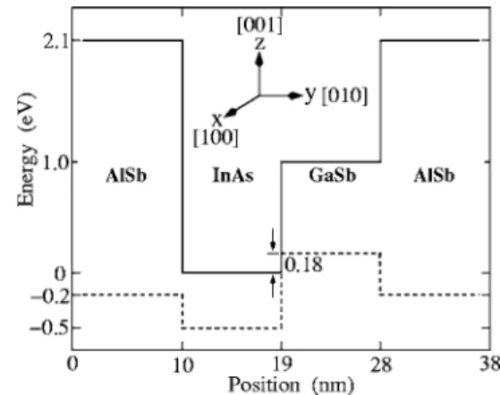
II. SUBBAND DISPERSIONS AND WAVE FUNCTIONS The AlSb/ InAs/ GaSb/ AlSb system to be studied in this paper is attached at both ends to two p-doped GaSb contacts which determine the local Fermi levels. In our numerical study, the acceptor concentration is set at 1018cm−3. For a specific sample with a 9 nm InAs layer, 9 nm GaSb layer, and 10 nm AlSb barriers, the band edges calculated with our self-consistent scheme共to be described in the next section兲 are shown in Fig. 1 with a solid line for the conduction band and a dashed line for the valence band. The crystal axes are also marked in Fig. 1, and we use the z axis to specify the quantization of spin and angular momentum. A weak dc cur-rent flows along the x axis. To study the spin polarization in the quantum well of this sample, we first need to calculate the subband dispersions and the corresponding wave func-tions self-consistently with the potential distribution and the Fermi level position.
We generalize the model used in Ref. 28 by including the effects of strain induced by the lattice mismatch. Let us de-fine as the angle between the dc current flow direc-tion共x axis兲 and the in-plane wave vector k储. Using the set
of basis functions u1=兩s1/2,1/2典, u2=兩p3/2,3/2典, u3=兩p3/2,−1/2典,
u4=兩p1/2,−1/2典, u5=兩s1/2,−1/2典, u6=兩p3/2,−3/2典, u7=兩p3/2,1/2典, and
u8=兩p1/2,1/2典, which is given in Ref. 25, the eight-band k·p Hamiltonian for= 0 has a block-diagonal form25
Hˆ =
冉
H ˆ + 0 0 Hˆ −冊
+冉
H ˆ ⑀ 0 0 Hˆ ⑀冊
. 共1兲The matrices Hˆ± depend on momentum operators, conduc-tion and valence band edges, split-off energies, interband momentum matrix elements, and the modified Luttinger pa-rameters. Their explicit forms are given in Ref. 25. The ma-trix Hˆ⑀represents the effects of strain, and can be obtained through a unitary transformation from the strain terms in the Hamiltonian given in Ref. 27. These terms include the con-duction and valence band deformation potentials, as well as the strain tensor with components ⑀ij. Since our sample is
grown along the y axis, ⑀xx=⑀zz and ⑀ij= 0 for i⫽ j. These
tensor components are also similarly defined as in Ref. 27 since our quantum well structure is grown on GaSb. We should point out that we have neglected in our model Hamil-tonian the linear-in-k terms and Kane’s B-parameter, result-ing from the lack of inversion symmetry in bulk zinc-blende crystals, since they are small.
Among the strain tensor components, the terms of the form kl⑀ijcan produce a significant spin split of the valence
band levels in the quantum well if the GaSb layer is strained.35 However, the heterostructures we study here are grown on GaSb, and so the GaSb layer in the quantum well is free from strain. Consequently such terms in the strain Hamiltonian have been neglected with no influence on the spin split of the hybridized electron-hole subbands and the spin polarization in our systems.
We call the two states for = 0 with opposite average spins sz the spin-up and spin-down states, and label them
by “⫹” and “⫺” respectively. Let the magnitude of k储
be k储⬅兩k储兩. For states with k储= kx, their envelope functions
+=关1234兴T and −=关5678兴T together with the
eigenenergy E satisfy the equation
共Hˆ±+ Hˆ⑀兲±共k储兲 = E±共k储兲. 共2兲
The corresponding total wave functions are then ⌿+共 = 0 , k储兲=兺i=14 uii for the spin-up states, and ⌿−共= 0 , k储兲
=兺i=58 uiifor the spin-down states. For the electronlike and
the heavy-hole-like states, the so-defined spin-up 共or spin-down兲 implies sz⬎0 共or sz⬍0兲. However, for light-hole-like
states spin-up implies sz⬍0 and spin-down sz⬎0. The above
equation will be solved together with the Poisson equation self-consistently in order to take into account the charge re-distribution. The modification of the potential profile along the x axis is negligibly small because the dc current is very weak. Hence, we can writeias i=¯ 共y兲exp共iki 储x兲.
For hybridized electron-hole states with small in-plane wave vectors k储 at the Fermi level, we can neglect the
sub-band anisotropy27 and use the scattering matrix method, which was clearly described in Refs. 25 and 28, to solve Eq. 共2兲. The subband anisotropy in InAs/GaSb quantum wells results mainly from the strong anisotropy of the three-dimensional共3D兲 hole dispersions of the bulk GaSb crystal due to the difference between the second and third Luttinger parameters. Such a difference influences considerably the level positions in the InAs/ GaSb quantum wells19and hence cannot be neglected. For the present two-dimensional 共2D兲 case, however, the subband anisotropy is small for small k储
as our calculations showed. This can be explained by consid-ering the in-plane vector k储as a projection of the 3D vector ki of ith bulk state, which contributes to the 2D state, onto
the interface plane. Roughly speaking, the 3D vector kiis a
sum of the k储and a normal “quantized” ki⬜that depends on
the well width. For a narrow well width and a small magni-tude of k储, we have k储Ⰶ兩ki⬜兩 and hence the 3D vector ki
varies within a small angular range as k储 rotates in a full
angular range of 2. For the small angular range of ki, the
dispersion is approximately isotropic although the anisotropy of 3D dispersions can be significant in a large angular range. Knowing the wave functions ⌿+共= 0 , k储兲 and ⌿−共
= 0 , k储兲, the wave functions of the states with finite ,
⌿+共, k储兲 and ⌿−共, k储兲, can be easily derived. For this
pur-pose we replace the x-z coordinates by a new x
⬘
-z⬘
coordi-nates such that the x⬘
axis is along k储 共namely, x⬘
= x cos+ z sin兲 and the y
⬘
axis coincides with the y axis. In the new coordinate system, we express the basis functions asui
⬘
. Then the total wave functions can be expressed as ⌿+共, k储兲=兺i=14
ui
⬘
¯ 共y兲exp共iki 储x⬘
兲 and ⌿−共, k储兲=兺i=58
ui
⬘
¯ 共y兲i⫻exp共ik储x
⬘
兲. By writing the basis functions ui⬘
in terms of thefunctions uiand the angle,37we obtain
⌿+共,k储兲 =
兺
i=1 8 ui兺
l=1 4 Aillexp关ik储共x⬘
− x兲兴, 共3兲 ⌿−共,k储兲 =兺
i=1 8 ui兺
l=5 8 Aillexp关ik储共x⬘
− x兲兴, 共4兲where the matrix A is
A =
冢
c 0 0 0 − s 0 0 0 0 c3冑
3cs2 0 0 − s3 −冑
3c2s 0 0冑
3cs2 c共c2− 2s2兲 0 0 −冑
3c2s 共2c2− s2兲s 0 0 0 0 c 0 0 0 s s 0 0 0 c 0 0 0 0 s3冑
3c2s 0 0 c3冑
3cs2 0 0冑
3c2s −共2c2− s2兲s 0 0冑
3cs2 c共c2− 2s2兲 0 0 0 0 − s 0 0 0 c冣
共5兲with c = cos共/ 2兲 and s=sin共/ 2兲. We should notice that when varies, the spin orientation of states with respect to the axis of quantization 共z axis兲 changes. Hence, the state ⌿+共, k储兲 关or ⌿−共, k储兲兴 and the state ⌿+共0,k储兲 关or ⌿−共0,k储兲兴
have the same average spin but with opposite signs. To sim-plify the writing, we will call⌿+共, k储兲 the spin-up state and
⌿−共, k储兲 the spin-down state.
III. SPIN POLARIZATION
In the absence of a dc current, the distribution function
f共E兲 of quasiparticles is reduced to its symmetric part fs共E兲.
At temperature T it is given as
fs共E兲 =
1
1 + exp关共E − EF兲/T兴
, 共6兲
where EFis the Fermi level. Then the spin polarization in the
quantum well is zero, because due to time reversal symmetry the contribution from the sz⬎0 states with k储 cancels that
from the sz⬍0 states with −k储. The dc current along the
x axis produces an asymmetric part of the distribution
func-tion fa+共E+,, k
储兲 for spin-up states, and fa
−共E−,, k
储兲 for
spin-down states. The energies E±共k
储兲 of the up and
spin-down states are self-consistent solutions of Eq. 共2兲 and the Poisson equation. If the level broadening⌬E⯝ប/, where is the momentum relaxation time, is much less than the level separation between the spin-up and the spin-down states, we can use the Boltzmann equation to calculate fa
±共E±,, k
储兲.
Under a weak dc current, 兩fa
±共E±,, k
储兲兩 are much smaller
than fs共E,, k储兲. Let e be the electron charge and vx±
=1បdEdk±
储 cos the group velocities of the up and
spin-down states. Under a weak electric field F along the x axis, we have fa ±共E±,,k 储兲 = 兩e兩Fvx ±fs共E,,k储兲 E . 共7兲
To calculate the density of spin polarization in the InAs/ GaSb quantum well, we assume that in the xz plane the sample is bounded spatially in the area 0艋x艋1 and 0艋z艋1. Along the y axis, the InAs layer is in the region 0 = y1e艋y艋y2e and the GaSb in the region y2e= y1h艋y艋y2h. In terms of the Pauli spin matrixz, the average values of
elec-tron spins 具se±典 for the spin-up and the spin-down states are
calculated as 具se±典 =
冕
y1e y2e dy冕
0 1 dx冕
0 1 dz⌿±†共,k储兲 1 2z⌿±共,k储兲. 共8兲 Similarly, the average values of hole spins 具sh±典 for the spin-up and the spin-down states are
具sh ±典 =
冕
y1h y2h dy冕
0 1 dx冕
0 1 dz⌿±†共,k储兲 1 2z⌿±共,k储兲. 共9兲 In terms of具se±典 and 具sh±典, the densities of spin polarization of electrons Se in the InAs layer and of holes Sh in the GaSblayer are then readily obtained as
Se,h= 1 共2兲2
冕
关fa +共E+,,k 储兲具se,h + 典 + f a −共E−,,k 储兲具se,h − 典兴k 储dk储d. 共10兲 If several subbands contribute to the spin polarization, then a summation should also be taken over all these subbands at the right side of Eq.共10兲.We define ±共, k储兲 as the eight-component envelope
⌿±共, k储兲. Then Eqs. 共8兲 and 共9兲 can be rewritten as 具se±典 =
冕
y1e y2e dy±†共,k储兲B±共,k储兲, 共11兲 具sh ±典 =冕
y1h y2h dy±†共,k储兲B±共,k储兲. 共12兲In the above equations, the 8⫻8 matrix B has a block-diagonal form B =1 2
冉
B+ 0 0 B−冊
, 共13兲where the 4⫻4 matrices B±are given by
B±=
冢
±1 0 0 0 0 ±1 0 0 0 0 ⫿1/3 ±2冑
2/3 0 0 ±2冑
2/3 ±1/3冣
. 共14兲Substituting具se,h± 典 from Eqs. 共11兲 and 共12兲, and fa±共E±,, k储兲
from Eq.共7兲 into Eq. 共10兲, using Eqs. 共3兲–共5兲 and integrating over the anglein Eq.共10兲, we obtain a compact expression for Se,has Se,h=兩e兩F 8ប
冕
冉
dE+ dk储 fs EGe,h + −dE− dk储 fs EGe,h −冊
k 储dk储, 共15兲 where Ge,h+ =冕
y1e,h y2e,h 共兩1兩2+兩2兩2−兩3兩2/3 +兩4兩2/3兲dy, 共16兲 and Ge,h− =冕
y1e,h y2e,h 共兩5兩2+兩6兩2−兩7兩2/3 +兩8兩2/3兲dy. 共17兲 We would like to remind the reader that the envelope func-tionsiin Eqs. 共16兲 and 共17兲 are the components of+共k储兲and−共k储兲, respectively, which are solutions of Eq. 共2兲 for
= 0.
We should point out that the growth direction of our sample is the y axis and that a weak electric field is applied along the x axis. The z axis is chosen to be the quantization axis of spin and angular momentum. In this case, similar model calculations do not indicate any spin polarization of electrons or holes along the x and y axes.
IV. RESULTS AND DISCUSSION
To perform numerical calculations we set the temperature at 1.5 K, the relaxation time= 10−11seconds, and the ap-plied parallel dc electric field 25 V / cm. The material param-eters and the band offsets are taken from Refs. 23 and 27.
Since the dispersions of AlSb/ InAs/ GaSb/ AlSb quantum wells are dominated by the InAs layer width We and the
GaSb layer width Wh, these two are the varying parameters
in our numerical study. The sample shown in Fig. 1 has
We= 9 nm and Wh= 9 nm. We should mention that the
asym-metric parts of the distribution functions fa±共E±,, k储兲 are
sig-nificant only near the Fermi level, and the spin polarization of the system is mainly contributed by the subbands around this energy region. Consequently, in our numerical results we will present only the lowest electronlike subband 1e and the highest heavy-hole-like subband 1hh in the quantum well. These subbands are labeled according to the wave-function properties of the corresponding states at zone center k储= 0.
The calculated dispersions are shown in Fig. 2共a兲 for 共We, Wh兲=共9,3兲 nm, and Fig. 2共b兲 for 共We, Wh兲=共9,9兲 nm.
The solid curves are for the spin-up states and the dashed curves are for the spin-down states. The electron-hole system
FIG. 1. The self-consistent energy band diagram of the AlSb/ InAs/ GaSb/ AlSb quantum well with a 9 nm InAs layer and a 9 nm GaSb layer. The solid curves are for the conduction band edge and the dashed curves are for the valence band edge.
FIG. 2. The 1e and 1hh subband dispersions in the InAs/ GaSb quantum well with a 9 nm InAs layer. The GaSb layer thickness is 3 nm for panel共a兲 and 9 nm for panel 共b兲. Inset in panel 共b兲 is a magnification of a neighborhood of the location where the Fermi level crosses the electronlike levels. The zero energy is set at the InAs conduction band edge at the AlSb/ InAs interface. Solid curves are for the spin-up states and dashed curves the spin-down states.
corresponding to Fig. 2共a兲 is in a normal semiconducting 共NSC兲 phase because the lowest electron level is higher than all hole levels. With increasing GaSb layer thickness Wh, the
1hh level at k储= 0 moves upwards, and eventually lies above
the 1e as shown in Fig. 2共b兲 for Wh= 9 nm. As the in-plane
wave vector k储 increases, the electronlike states and the
heavy-hole-like states approach each other and anticross, re-sulting in a hybridization gap in the in-plane dispersions. After the anticrossing, the 1hh subband becomes electronlike while the 1e subband becomes heavy-hole-like. Such a sys-tem is in a hybridized semiconducting 共HSC兲 phase. The Fermi level EFcrosses only the 1e subband in Fig. 2共a兲, and
only the 1hh subband in Fig. 2共b兲 as shown by the inset. Hence, the main contribution to the spin polarization is from the 1e subband for the sample with Wh= 3 nm, but from the
1hh subband for the sample with Wh= 9 nm.
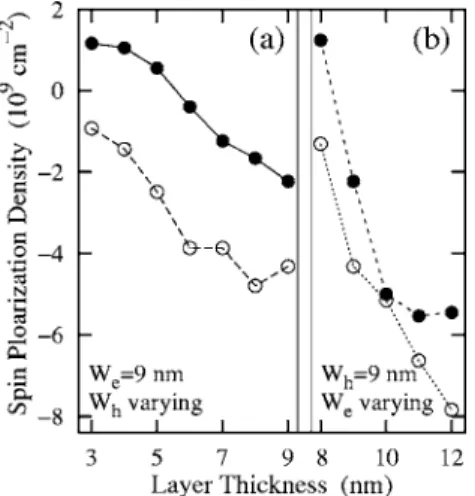
To investigate in details the effect of InAs and GaSb layer widths, we have calculated the spin-polarization density with fixed We= 9 nm共or Wh= 9 nm兲 but varying Wh共or We兲. The
results are shown in Fig. 3 with solid dots for the electron spin polarization in the InAs layer and open circles for the hole spin polarization in the GaSb layer. Figure 3共a兲 is for constant We= 9 nm and Fig. 3共b兲 is for constant Wh= 9 nm. It
is important to notice in Fig. 3共a兲 a finite value of hole spin polarization even in the NSC for Wh= 3 nm, where almost all
holelike states are occupied by electrons. The origin of this hole spin polarization is the hybridization of the electronlike states with the light-hole states.23Around W
h⯝5.5 nm where
the system transforms from the NSC phase to the HSC phase, the electron spin polarization changes sign from posi-tive to negaposi-tive. This is because the spin-splitting of the elec-tronlike levels near the Fermi energy changes sign, as indi-cated in Fig. 2共b兲. On the other hand, the hole spin polarization remains negative in both the NSC and HSC phases. For the two phases in Fig. 3共a兲 with Wh= 3 nm and Wh= 9 nm, the signs of the total spin polarization are also
different.
For a fixed GaSb layer thickness at Wh= 9 nm, the NSC to
HSC phase transition occurs when the InAs layer width We
increases to about 8.5 nm. When We is reduced to 7.5 nm,
the Fermi level moves into the semiconducting gap, and so the total spin polarization of the entire system vanishes. As shown in Fig. 3共b兲, when Weincreases across the NSC-HSC
phase boundary, the electron spin polarization changes sign but not the hole spin polarization. We found several interest-ing phenomena. Because of its larger spin split, the hybrid-ized electronlike states give the main contribution to the spin polarization in both the InAs and GaSb layers. Also, in the HSC phase, because the electron spin polarization of the spin-up states almost compensates that of the spin-down states, the electron spin polarization is less than the hole spin polarization. Finally, the hybridization of electrons and holes for up states differs significantly from that for spin-down states, resulting in a strong spin polarization in the GaSb layer.
Similar to the plots in Fig. 3 for the spin-polarization density, plots of carrier concentration are shown in Fig. 4 with solid dots for the electron concentration n in the InAs layer and open circles for the hole concentration p in the GaSb layer. In all samples specified in this figure, n is larger than p. Due to hybridization of the empty electronlike states with the light-hole states,23,25there exists a small finite hole concentration in the NSC phase. With increasing GaSb layer width Whin Fig. 4共a兲, the 1hh level at k储= 0 moves to above
the Fermi energy. Hence, p increases with Whbut n remains
almost unchanged. On the other hand, with increasing InAs layer width Wein Fig. 4共b兲, n increases rapidly because the
1e level moves to lower energy. Such process of lowering the 1e level also increases p for the reason that electrons can flow into the InAs layer not only from the GaSb contacts but also from the GaSb valence band in the quantum well.
With increasing both the InAs layer thickness and the GaSb layer thickness, the semimetallic phase can be realized. Then there is no forbidden energy interval in the in-plane dispersion. The semimetallic phase can be achieved at zero bias for the quantum well with a 15 nm InAs layer and a 10 nm GaSb layer as our calculations showed. In this case
FIG. 3. Spin polarization density of electrons in the InAs layer 共solid dots兲 and of holes in the GaSb layer 共open circles兲 as func-tions of the layer thickness. For panel共a兲 the InAs layer is 9 nm but with varying GaSb layer width, and for panel共b兲 the GaSb layer is 9 nm but with varying InAs layer width.
FIG. 4. Electron concentration in the InAs layer共solid dots兲 and hole concentration in the GaSb layer共open circles兲 as functions of the layer thickness. For panel共a兲 the InAs layer is 9 nm but with varying GaSb layer width, and for panel共b兲 the GaSb layer is 9 nm but with varying InAs layer width.
the hybridization gaps for the spin-up and spin-down states do not overlap. Also, with increasing in-plane wave vector, the spin split of 1hh subband states, which contribute to most of the spin polarization, changes sign twice. As a result, our model gives a positive spin polarization of electrons in the InAs layer and a negative spin polarization of holes in the GaSb layer for this structure. However, when the layer gets thicker, the in-plane wave vector k储 of electronlike states at
the Fermi level gets larger and its magnitude can become comparable to the magnitudes of the 3D wave vectors of hole bulk states in the GaSb layer, which contribute to the 2D electronlike states. Hence, to derive accurate results of spin polarization, the anisotropy of subband dispersions should be been taken into account in our calculations.
Let us define the fraction of spin-polarized carriers e=兩Se兩/nsz
e
for electrons, and h=兩Sh兩/psz h
for holes, where
sze,h=
1
2. From Figs. 3 and 4, we see that for the parameters used in our calculation, botheandhare of the order of 1%.
However, Eq. 共15兲 indicates that the fraction of spin-polarized carriers can be easily enhanced by applying a stronger dc electric field. On the other hand, when the elec-tric field becomes sufficiently large, the drift velocities of the hybridized electron-hole states become of the same order as the corresponding group velocities. The approximation of small asymmetry of the distribution function is no longer valid and the scattering processes between the spin-up and spin-down states will decrease the spin polarization. Hence, the 100% spin polarization cannot be achieved by increasing the dc electric field. We believe that the maximum value of spin polarization, which can be achieved in the broken-gap quantum wells, is greater than that in type I asymmetric het-erostructures, because the spin-dependent hybridization of electron and hole states can significantly enhance the spin polarization.
Let us discuss the validity of the approximations used in our study of the quasiparticle spin polarization. First, corre-sponding to the momentum relaxation time = 10−11s, the electron mobility is about 105 cm2/共Vs兲 and the hole mobil-ity about 104cm2/共Vs兲. Then, at a field strength
F⯝25 V/cm, the drift velocity is about 106 cm/ s for elec-trons and 105 cm/ s for holes. Since these drift velocities are much less than the corresponding group velocities at the Fermi energy, our approximation of small asymmetry of the distribution function is valid.
We have neglected the bulk asymmetry terms which are proportional to Kane’s B parameter. It was shown in Ref. 8 that if the in-plane wave vectors are larger than 0.3 nm−1, the effect of these terms on the spin split of electron levels can-not be ignored. However, for the quantum wells studied here, the Fermi wave vector is about 0.1 nm−1. Consequently, the spin split due to these bulk asymmetry terms is at least one order of magnitude less than that produced by the Rashba effect for all states which contribute to the spin polarization. Finally, for= 10−11s, the corresponding level broadening is less than 0.1 meV. Therefore we can use the Boltzmann equation to calculate spin polarization. However, in low quality samples with higher defect concentration, the carrier mobility can be suppressed.38 In this situation the level broadening is large and so quantum kinetic theory should be used to study the spin polarization.
To close this section, we will outline two possible experi-mental detections of spin polarization in the InAs/ GaSb quantum wells. The first one involves the investigation of the frequency shift of nuclear magnetic resonance共NMR兲 in our samples. Such a method was proposed in Ref. 3 to detect the electron spin polarization in type I quantum wells with a lateral current. Since the wave function of the conduction band electron has a large component of s-type functions, it has a finite value at the location of each constitutive atom. Hence, there is a contact interaction between an electron spin and spins of Ga and In nuclei in the heterostructure. The corresponding shift in NMR frequency can be observed ex-perimentally, if the concentration of spin-polarized electrons is sufficiently high. The spins of holes, whose wave func-tions have large components of p-type funcfunc-tions, can also interact with the nuclear spins through the dipole-dipole in-teraction. Also, the holes in our structures are hybridized with the electrons. Hence, the contact interaction between the spins of holelike states and nuclei is finite.
The second approach, which is sensitive even for weak spin polarization of carriers in the quantum wells, is the op-tical method. It was proposed in Ref. 5 that the electron spin polarization in type-I quantum wells can be detected by mea-suring the polarization of photons emitted during the electron-hole recombination. The probability of the emitted light being right-handed or left-handed circular polarized de-pends on the occupation probability of various electron spin states. Similarly, in the quantum wells with spin-split sub-bands, the interband or intersubband absorption of circular polarized light by carriers also depends on the occupation probability of their spin states.39 Then, for a quantum well with spin-polarized carriers, its absorption coefficient for the right-handed circular polarized light is different from that for the left-handed circular polarized light. Such a difference can be observed experimentally. It is important to notice that the spin polarization of quasiparticles near the Fermi level is much stronger than the average spin polarization. Hence, by a proper tuning of the light frequency to select the optical transitions from the states near the Fermi level, the detected carrier spin polarization can be enhanced.
V. CONCLUSION
We have developed a theory of the spin polarization of quasiparticles in nonmagnetic asymmetric quantum wells un-der a dc current parallel to interfaces. We have used the eight-band k · p model including coupling of electron states, light-hole states, heavy-hole states, and the states in the split-off band. The spin split of subbands due to the spin-orbit interaction and the structure asymmetry, together with the existence of nonequilibrium distribution function of carriers, have generated interesting phenomena which are studied in details. Assuming a small asymmetry of the distribution functions our theory is based on solving the Boltzmann equa-tion for the hybridized electron-hole states. To present accu-rate numerical results, we have analyzed the spin polariza-tions of electrons and holes in InAs/ GaSb quantum wells. We have demonstrated the important effect of electron-hole
hybridization on the spin polarizations in both the InAs layer and the GaSb layer. For a very weak asymmetry of the dis-tribution function, the spin polarization of both electrons and holes can reach about 1%.
ACKNOWLEDGMENT
This work was financially supported by the RFBR共Grant No. 03-02-16788兲.
1Semiconductor Spintronics and Quantum Computation, edited by D. D. Awschalom, D. Loss, and N. Samarth共Springer-Verlag, Berlin, 2002兲; G. Schmidt, J. Phys. D 38, R107 共2005兲. 2F. T. Vasko and N. A. Prima, Sov. Phys. Solid State 21, 994
共1979兲.
3V. M. Edelstein, Solid State Commun. 73, 233共1990兲.
4A. G. Aronov, Yu. B. Lyanda-Geller, and G. E. Pikus, Zh. Eksp. Teor. Fiz. 100, 973共1991兲.
5A. G. Mal’shukov and K. A. Chao, Phys. Rev. B 65, 241308 共2002兲.
6Jun-ichiro Inoue, Gerrit E. W. Bauer, and Laurens W. Molen-kamp, Phys. Rev. B 67, 033104共2003兲.
7E. G. Mishchenko, A. V. Shytov, and B. I. Halperin, Phys. Rev. Lett. 93, 226602共2004兲.
8I. Vurgaftman and J. R. Meyer, Phys. Rev. B 70, 115320共2004兲. 9R. Winkler, Phys. Rev. B 70, 125301共2004兲.
10R. Winkler, Phys. Rev. B 71, 113307共2005兲.
11A. Zakharova, F. T. Vasko, and V. Ryzhii, J. Phys.: Condens. Matter 6, 7537共1994兲.
12A. Voskoboynikov, S. S. Liu, C. P. Lee, and O. Tretyak, J. Appl. Phys. 87, 387共2000兲.
13M. Kohda, Y. Ohno, Y. Takamura, F. Matsukora, and H. Ohno, Jpn. J. Appl. Phys., Part 2 40, L1274共2001兲.
14David Z.-Y. Ting and X. Cartoixa, Phys. Rev. B 68, 235320 共2003兲.
15I. Vurgaftman and J. R. Meyer, Phys. Rev. B 67, 125209共2003兲. 16A. G. Petukhov, D. O. Demchenko, and A. N. Chantis, Phys. Rev.
B 68, 125332共2003兲.
17M. M. Glazov, P. S. Alekseev, M. A. Odnoblyudov, V. M. Chistyakov, S. A. Tarasenko, and I. N. Yassievich, Phys. Rev. B
71, 155313共2005兲.
18P. Krstajic and F. M. Peeters, Phys. Rev. B 71, 115321共2005兲. 19A. Zakharova, K. Nilsson, K. A. Chao, and S. T. Yen, Phys. Rev.
B 72, 115329共2005兲.
20M. Altarelli, Phys. Rev. B 28, 842共1983兲.
21Y. Naveh and B. Laikhtman, Appl. Phys. Lett. 66, 1980共1995兲.
22A. J. L. Poulter, M. Lakrimi, R. J. Nicholas, N. J. Mason, and P. J. Walker, Phys. Rev. B 60, 1884共1999兲.
23E. Halvorsen, Y. Galperin, and K. A. Chao, Phys. Rev. B 61, 16743共2000兲.
24R. Magri, L. W. Wang, A. Zunger, I. Vurgaftman, and J. R. Meyer, Phys. Rev. B 61, 10235共2000兲.
25A. Zakharova, S. T. Yen, and K. A. Chao, Phys. Rev. B 64, 235332共2001兲.
26R. Magri and A. Zunger, Phys. Rev. B 65, 165302共2002兲. 27A. Zakharova, S. T. Yen, and K. A. Chao, Phys. Rev. B 66,
085312共2002兲.
28I. Lapushkin, A. Zakharova, S. T. Yen, and K. A. Chao, J. Phys.: Condens. Matter 16, 4677共2004兲.
29M. Lakrimi, S. Khym, R. J. Nicholas, D. M. Symons, F. M. Peeters, N. J. Mason, and P. J. Walker, Phys. Rev. Lett. 79, 3034 共1997兲.
30M. J. Yang, C. H. Yang, B. R. Bennett, and B. V. Shanabrook, Phys. Rev. Lett. 78, 4613共1997兲.
31L. J. Cooper, N. K. Patel, V. Drouot, E. H. Linfield, D. A. Ritchie, and M. Pepper, Phys. Rev. B 57, 11915共1998兲.
32M. J. Yang, C. H. Yang, and B. R. Bennett, Phys. Rev. B 60, R13958共1999兲.
33E. I. Rashba, Sov. Phys. Solid State 2, 1109共1960兲; Yu. A. By-chkov and E. I. Rashba, JETP Lett. 39, 78共1984兲.
34X. Cartoixa, D. Z.-Y. Ting, and T. C. McGill, Phys. Rev. B 68, 235319共2003兲.
35O. Mauritz, and U. Ekenberg, Phys. Rev. B 55, 10729共1997兲. 36J. Luo, H. Munekata, F. F. Fang, and P. J. Stiles, Phys. Rev. B 38,
R10142共1988兲; 41, 7685 共1990兲.
37E. L. Ivchenko and G. E. Pikus, Superlattices and Other
Hetro-structures共Springer, Berlin, 1997兲.
38K. Suzuki, S. Miyashita, and Y. Hirayama, Phys. Rev. B 67, 195319共2003兲.
39S. D. Ganichev and W. Prettl, J. Phys.: Condens. Matter 15, R935 共2003兲.