Stress-induced morphology and fine-line stability enhancement of NiSi on poly-SiGe
with a buffer polycrystalline silicon interlayer
Chi-Chang Wu, Wen-Fa Wu, Fu-Hsiang Ko, Hsin-Chiang You, and Wen-Luh Yang
Citation: Applied Physics Letters 92, 182106 (2008); doi: 10.1063/1.2920202 View online: http://dx.doi.org/10.1063/1.2920202
View Table of Contents: http://scitation.aip.org/content/aip/journal/apl/92/18?ver=pdfcov Published by the AIP Publishing
Articles you may be interested in
Thermal stability of supercritical thickness-strained Si layers on thin strain-relaxed buffers J. Appl. Phys. 102, 123502 (2007); 10.1063/1.2825042
Effect of Mo interlayer on thermal stability of polycrystalline NiSi thin films J. Appl. Phys. 101, 063544 (2007); 10.1063/1.2714490
Formation of nickel silicide and germanosilicide layers on Si(001), relaxed Si Ge Si ( 001 ) , and strained Si/relaxed Si Ge Si ( 001 ) and effect of postthermal annealing
J. Vac. Sci. Technol. A 24, 1468 (2006); 10.1116/1.2210942
Ge fraction dependent improved thermal stability of in situ doped boron in polycrystalline Si 1 x Ge x ( 0 x 0.5 ) films on SiON
J. Appl. Phys. 97, 054909 (2005); 10.1063/1.1854731
F-enhanced morphological and thermal stability of NiSi films on BF 2 + -implanted Si(001) Appl. Phys. Lett. 81, 5138 (2002); 10.1063/1.1533856
This article is copyrighted as indicated in the article. Reuse of AIP content is subject to the terms at: http://scitation.aip.org/termsconditions. Downloaded to IP: 140.113.38.11 On: Wed, 30 Apr 2014 23:05:31
Stress-induced morphology and fine-line stability enhancement
of NiSi on poly-SiGe with a buffer polycrystalline silicon interlayer
Chi-Chang Wu,1,2 Wen-Fa Wu,2,a兲 Fu-Hsiang Ko,1,b兲 Hsin-Chiang You,3 and Wen-Luh Yang4
1
Institute of Nanotechnology and Department of Materials Science and Engineering, National Chiao Tung University, Hsinchu 300, Taiwan
2
National Nano Device Laboratories, Hsinchu 300, Taiwan
3
Department of Computer Science and Information Engineering, Asia University, Taichung 413, Taiwan
4
Department of Electronic Engineering, Feng Chia University, Taichung 407, Taiwan
共Received 14 January 2008; accepted 16 April 2008; published online 9 May 2008兲
The thermal and morphological stability of NiSi is enhanced by inserting a polycrystalline共poly-Si兲 buffer layer between the Ni and poly-SiGe films. NiSi films formed on poly-Si/poly-SiGe stack layers possessed continuous, smooth structures after annealing at 500– 850 ° C. Moreover, nickel germanosilicide关Ni共Si, Ge兲兴 lines formed on the poly-SiGe exhibited a fine-line effect, i.e., the sheet resistance increased upon decreasing the linewidth, whereas the sheet resistance of NiSi lines formed on the poly-Si/poly-SiGe stack layers remained less than 5 ⍀/square. A model for the stress-confined grain growth and recrystallization is proposed to explain the improved properties of the poly-Si-buffered film. © 2008 American Institute of Physics. 关DOI:10.1063/1.2920202兴
Nickel self-aligned silicidation 共NiSi兲 is a critical pro-cess used to diminish contact resistance prior to metal inter-connection in ultralarge-scale integration technology. This silicidation process is particularly important when the device dimensions are less than 100 nm. The formation of NiSi on gate electrodes improves the driving current and transcon-ductance 共Gm兲 of metal oxide semiconductor field effect transistor devices.1
Polycrystalline silicon-germanium共poly-SiGe兲 is a suit-able candidate material for replacing polycrystalline silicon 共poly-Si兲 at the gate electrode because of its lower dopant activation energy, higher carrier mobility,2and good compat-ibility with standard silicon complementary metal-oxide semiconductor processing technologies, as well as the possi-bility of tuning its work function merely by changing the mole fraction of Ge.3 In addition, poly-SiGe films can be deposited at temperatures lower than those required for poly-Si films, presumably because of the lower binding en-ergies of the Si–Ge and Ge–Ge bonds in poly-SiGe films relative to those of the Si–Si bonds in poly–Si films.4 Unfor-tunately, combining nickel silicide processing with poly-SiGe materials suffers from the drawback that the direct re-action between nickel and poly-SiGe provides materials exhibiting relatively poor morphological stability relative to those obtained from poly-Si 共Ref. 5兲 because the melting point of the ternary alloy Ni共Si, Ge兲 is lower than that of NiSi. This problem restricts the further application of nickel silicide and poly-SiGe gate materials.
In this paper, we compare the morphological stabilities and fine-line effects of Ni/poly-Si/SiO2/Si-substrate, Ni/poly-SiGe/SiO2/Si-substrate, and Ni/poly-Si/poly-SiGe/
SiO2/Si-substrate systems. We studied the effects of the
sil-icidation temperature on the sheet resistance of various films. In addition, we examined the fine-line effects of nickel 共ger-mano兲 silicided narrow lines. Although it has been reported that the resistance of NiSi formed on poly-Si lines exhibits
independent geometrical dimensions,6no literature exists de-scribing the electrical properties of Ni共Si, Ge兲 formed on narrow poly-SiGe lines. Thus, we evaluated the morphology and recrystallization effects of these films, and propose a model that accounts for the stress-induced grain growth sup-pression and recrystallization effects.
These experiments employed 6 in.共100兲-oriented silicon wafers. A 500 nm thick silicon oxide film was first formed, followed by the deposition of a共1兲 200 nm poly-Si film, 共2兲 200 nm poly-SiGe layer, or共3兲 40 nm Si/160 nm poly-SiGe stack layer. After Radio Corporation of America共RCA兲 standard cleaning, 10 nm Ni and 4 nm TiN films were de-posited through dc sputtering. After metal deposition, the Ni-silicidation reaction was performed in a rapid thermal an-nealing system. Finally, a mixture of H2SO4and H2O2共3:1兲
was used to selectively remove the unreacted metal at a tem-perature of 120 ° C. The sheet resistance of the silicide film was determined using a four-point probe system. A bridge structure was used in conjunction with an Agilent 4156A semiconductor analyzer to characterize the values of resis-tance of various narrow lines. The morphology of the film was examined using transmission electron microscopy 共TEM兲. The stresses of these films were measured using a Tencor FLX-2320 instrument.
After performing the silicidation reaction, the stacked 共1兲 Ni/poly-Si/SiO2/Si-substrate, 共2兲 Ni/poly-SiGe/
SiO2/Si-substrate, and 共3兲 Ni/poly-Si/poly-SiGe/SiO2/
Si-substrate films were transformed into 共i兲 NiSi/poly-Si/SiO2/Si-substrate, 共ii兲 Ni共Si1−xGex兲/poly-SiGe/SiO2/
Si-substrate, and共iii兲 NiSi/poly-SiGe/SiO2/Si-substrate spe-cies, respectively. The phase for sample共iii兲 was identified to be NiSi by x-ray diffraction. Figure1共a兲provides a compari-son of the sheet resistances of these films as a function of the annealing temperature. The sheet resistances of samples 共i兲 and共ii兲 slightly increased upon increasing the annealing tem-perature over the range 500– 800 ° C and then abruptly in-creased at temperatures higher than 850 ° C. In contrast, the resistance of sample共iii兲 remained constant after annealing at temperatures between 500 and 850 ° C. This observation sug-a兲Electronic mail: [email protected].
b兲Electronic mail: [email protected].
APPLIED PHYSICS LETTERS 92, 182106共2008兲
0003-6951/2008/92共18兲/182106/3/$23.00 92, 182106-1 © 2008 American Institute of Physics
This article is copyrighted as indicated in the article. Reuse of AIP content is subject to the terms at: http://scitation.aip.org/termsconditions. Downloaded to IP: 140.113.38.11 On: Wed, 30 Apr 2014 23:05:31
gests that the insertion of the buffer film, i.e., poly-Si, be-tween the Ni and poly-SiGe films was beneficial to the elec-trical and thermal properties.
Figure1共b兲displays the sheet resistances of various nar-row lines of samples共i兲–共iii兲 annealed at 600 °C. The sheet resistance of lines of sample共i兲 remained nearly constant for linewidths ranging from 200 to 100 nm, which is consistent with previous findings.7The slight decrease in resistance that occurred after shrinking the linewidth from 100 to 60 nm was caused by edge effects of the recessed spacer forming a thicker silicide at the line’s edge.8In contrast, the sheet re-sistance for sample 共ii兲 increased upon reducing the line-width. This phenomenon, the well-known fine-line effect, had been reported from a study of Ti silicide,9but has never been reported for Ni共Si, Ge兲 lines formed on poly-SiGe. The fine-line effect vanished after insertion of poly-Si, i.e., for sample 共iii兲. This behavior should improve the process sta-bility of such systems, especially for sub-100 nm devices. We infer that the larger Ni共Si, Ge兲 grains resulting from the ready grain growth of poly-SiGe after annealing was the main cause of the increased sheet resistance in sample 共ii兲. Similar behavior resulting from grain size effects has been previously described.10
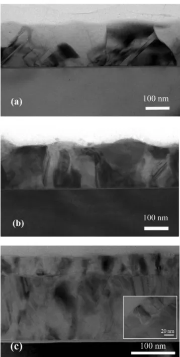
Figure 2 displays cross-sectional TEM micrographs of the silicide films obtained after annealing at 850 ° C. Samples共i兲 and 共ii兲 关Figs.2共a兲and 2共b兲, respectively兴 pos-sessed completely agglomerated silicide structures that were responsible for the poor electrical properties observed in Fig.1. These images also reveal the occurrence of layer in-version, i.e., the reversal of the positions of the silicide and poly-Si共Ge兲 layers, which is consistent with previous findings.11These agglomerated silicide islands resulted from poly-Si共Ge兲 grain growth and a recrystallization effect
dur-ing treatment at high temperatures. Moreover, Chen et al. have reported that the Ge segregation effect of Ni共Si, Ge兲 would result in a more severe thermal stability problem for Ni共Si, Ge兲 formed on poly-SiGe.12
The segregation of Ge from Ni共Si, Ge兲 grains is driven by the heat of formation for NiSi being more favorable than that of NiGe. In contrast, the grains in sample共iii兲 retained their columnar structure and a uniform interface existed between the silicide and poly-SiGe 关see Fig. 2共c兲and its inset兴. The uniform interface is likely caused by the Ge, which is expelled from the Ni–Si–Ge com-pound, blocked the Ni diffusion paths, and resulted in the delay in the formation of NiSi2.13,14Similar results were also
reported for CoSi2 formed on a SiGe layer.15This
observa-tion implies that the inserobserva-tion of the poly-Si film in sample 共iii兲 maintained the film’s continuance and curtailed agglom-eration in the silicide film.
In Fig. 3, we propose a model to explain the stress-induced grain growth suppression of the silicide film. In
FIG. 1.共a兲 Sheet resistances of the nickel 共germano兲silicide films formed on poly-Si关sample 共i兲兴, poly-SiGe 关sample 共ii兲兴, and poly-Si/poly-SiGe stack layers关sample 共iii兲兴 as a function of the annealing temperature. 共b兲 Sheet resistances of the nickel关germano兴silicide lines annealed at 600 °C as a function of the linewidth.
FIG. 2. Cross-sectional TEM micrographs of the nickel共germano兲silicide films formed on共a兲 poly-Si 关sample 共i兲兴, 共b兲 poly-SiGe 关sample 共ii兲兴, and 共c兲 poly-Si/poly-SiGe stack layers关sample 共iii兲兴 after annealing at 850 °C.
182106-2 Wu et al. Appl. Phys. Lett. 92, 182106共2008兲
This article is copyrighted as indicated in the article. Reuse of AIP content is subject to the terms at: http://scitation.aip.org/termsconditions. Downloaded to IP: 140.113.38.11 On: Wed, 30 Apr 2014 23:05:31
terms of thermodynamics, the driving force for the morpho-logical transformation of a grain is the reduction in interfa-cial energy. Figure3共a兲schematically displays the morphol-ogy changes that occurred to samples 共i兲 and 共ii兲 after annealing. Increasing the annealing temperature enhances the sizes of the poly-Si and poly-SiGe grains, with the silicide migrating along the grain boundary, ultimately resulting in agglomerated island and layer inversion occurring at exces-sively high temperatures.16 Figure3共b兲provides an explana-tion of the benefit of inserting the poly-Si film into sample 共iii兲. The underlying poly-SiGe layer exerts a compressive stress upon the upper poly-Si film. This stress suppressed the grain growth of the poly-Si and silicide, which in turn re-tarded the agglomeration and layer inversion effects. In ad-dition, the Ge layer between the silicide and poly-SiGe film also play the role to retard layer inversion.13–15 This model can also explain the behavior of the Ni共Si, Ge兲 fine lines of sample共ii兲. The thermal stability of silicided-narrow lines is determined by the laterally confined areas, and larger grains induce linewidth-dependent degradation.17 Larger silicide grains readily formed columnar structures and then con-verted into bamboolike structures as the linewidth shrank. Agglomeration into islands then occurred during annealing. For sample 共iii兲, the fine-line effect was eliminated in the
presence of the inserted poly-Si layer because of suppression in the growth of silicide grains. Therefore, the formation of bamboolike structures was retarded.
To support this model with respect to the stress effect in sample共iii兲, we prepared three samples having various poly-SiGe film thicknesses. We found that samples possessing smaller compressive stresses exhibited inferior electrical properties after annealing at high temperatures, especially when the annealing temperature exceeded 850 ° C. This find-ing is consistent with our prediction that compressive stress enhances the thermal and morphological stabilities of nickel silicide samples.
In conclusion, we have investigated the thermal stability and electrical behavior of various nickel 共germano兲 silicide structures. The insertion of a poly-Si film on the poly-SiGe significantly enhances the thermal and morphological stabili-ties of NiSi films. We have derived a stress-confined grain growth and Ge blocking model to explain the beneficial ef-fects of the poly-Si film and confirm the predictions made after scrutiny of TEM images. The presence of poly-Si films improved the properties of both the thin-film and fine-line NiSi structures.
1C. C. Wu, W. F. Wu, P. Y. Su, L. J. Chen, and F. H. Ko,Microelectron.
Eng. 84, 1801共2007兲.
2X. Yu, C. Zhu, and M. Yu,Appl. Phys. Lett. 89, 163508共2006兲. 3J. Huang, N. Wu, Q. Zhang, C. Zhu, M. F. Li, A. A. O. Tay, Z. Y. Cheng,
C. W. Leitz, and A. Lochtefeld,Appl. Phys. Lett. 88, 143506共2006兲. 4M. Mitsui, K. Arimoto, J. Yamanaka, and K. Nakagawa,Appl. Phys. Lett.
89, 192102共2006兲.
5J. Seger, T. Jarmar, Z. B. Zhang, H. H. Radamson, F. Ericson, U. Smith, and S. L. Zhang,J. Appl. Phys. 96, 1919共2004兲.
6Y. He, X. L. Liu, J. Y. Feng, and Q. L. Wu,J. Appl. Phys. 96, 6928 共2004兲.
7H. Iwai, T. Ohguro, and S. I. Ohmi,Microelectron. Eng. 60, 157共2002兲. 8Q. Xiang, C. Woo, E. Paton, J. Foster, B. Yu, and M. R. Lin, IEEE
Conference Proceedings, 2000 Symposium on VLSI Technology, Digest of Technical Papers, p. 76共2000兲.
9S. L. Zhang and U. Smith,J. Vac. Sci. Technol. A 22, 1361共2004兲. 10R. W. Mann, G. L. Miles, T. A. Knotts, D. W. Rakowski, L. A. Clevenger,
J. M. E. Harper, F. M. d’Heurle, and C. Cabral, Jr.,Appl. Phys. Lett. 67, 3729共1995兲.
11T. Jarmar, J. Seger, F. Ericson, D. Mangelinck, U. Smith, and S.-L. Zhang,
J. Appl. Phys. 92, 7193共2002兲.
12L. J. Chen, J. B. Lai, and C. S. Lee,Micron 33, 535共2002兲.
13W. W. Wu, S. L. Cheng, S. W. Lee, and L. J. Chen,J. Vac. Sci. Technol.
B 21, 2147共2003兲.
14W. W. Wu, J. H. He, S. L. Cheng, S. W. Lee, and L. J. Chen,Appl. Phys.
Lett. 83, 1836共2003兲.
15W. W. Wu, T. F. Chiang, S. L. Cheng, S. W. Lee, L. J. Chen, Y. H. Peng, and H. H. Cheng,Appl. Phys. Lett. 81, 820共2002兲.
16P. S. Lee, K. L. Pey, D. Mangelinck, J. Ding, D. Z. Chi, J. Y. Dai, and L. Chan,J. Electrochem. Soc. 149, 331共2002兲.
17K. Maex,Mater. Sci. Eng., R. 11, 53共1993兲. FIG. 3. Schematic models of nickel共germano兲silicide formation at high
annealing temperatures:共a兲 on poly-Si 关sample 共i兲兴 and poly-SiGe 关sample 共ii兲兴 and 共b兲 on poly-Si/poly-SiGe stack layers 关sample 共iii兲兴.
182106-3 Wu et al. Appl. Phys. Lett. 92, 182106共2008兲
This article is copyrighted as indicated in the article. Reuse of AIP content is subject to the terms at: http://scitation.aip.org/termsconditions. Downloaded to IP: 140.113.38.11 On: Wed, 30 Apr 2014 23:05:31