98
/
CLEO'99
/
TUESDAY MORNING
CTu14 1 1 1 5 am
GaN characterlzations using femtosecond optical pulses Chi-Kuang Sun, Yong-Liang Huang, Jiun-Cheng Wang, Stacia Keller,* Michael P. Mack,* U.K. Mishra,* Steven P. DenBaars,' Institute of Electro- Optical Engineering, National Taiwan University, Taipei 10617, Taiwan R.O.C.; E-mail: sunC3cc.ee.n tu.edu.tw
The demonstration of high-brightness green- UV light-emitting diodes and laser diodes has established GaN as key materials for optoelec- tronics operating in the green-UV wavelength range.' Despite the progress in the device de- velopments, the basic properties of GaN are still poorly understood. Due to their high peak powers and short pulse widths, femtosecond optical pulses have become major tools for material characterization. In this presentation, we will report on the characterization of GaN using femtosecond optical pulses. First, we have measured below bandgap nonlinear re- fractive index n2 using 2-scan techniques.2 High n2 value on the order of - cm2/W was measured, which indicates potential appli- cations in all optical control and ultrafast op- toelectronics. Second, we have measured two photon absorption coefficient
(p2)
using pulsewidth autocorrelation. The measuredp2
is on the order of 3 cm/GW (for midgap wave- lengths), which is higher than that of diamond and one order of magnitude larger than that of fused silica. The large two-photon absorption coefficients and broad band applicability make GaN and related materials excellent candidates as nonlinear crystals for I R - W femtosecond pulsewidth measurements. Third, using fem- tosecond thermomodulation spectroscopy, we have studies the bandtail states in heavily n-typed doped GaN samples. The experimen- tal results agree well with a model proposed by P.K. Chakraborty and J.C. Bi~was.~The GaN film was grown by MOCVD on c-plane sapphire in an atmospheric pressure reactor. After annealing the substrate at 1050°C, a 525-a-thick nucleation layer was deposited at 600°C. The temperature was then raised to 1080°C to grow unintentionally doped GaN layer of 2 p m thickness. The re- sulting n-type carrier concentration was 1.2 x
10'' ~ m - ~ . The measured electrical mobility constant was 620 cm2/V-s, indicating excel- lent epitaxial quality. For highly doped samples, Si doped GaN layer of 1000 nm thick-
1 .J4
1
1.021 1 .M) 0.98 1 0.96 -1.5 -1.0 -0.5 0.0 0.5 1.0 1.5 Z (mm)CTuI4 Fig. 1. Normalized 2-scan transmit- tance of GaN measured using femtosecond pulses
at A = 367.5 nm. The solid line is a theoretical fit.
k720 nrn
-0.3 -0.2 -0.1 0.0 0.1 0.2 0.3
Delay (PS)
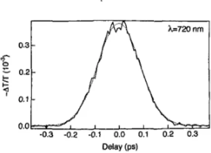
CTuI4 Fig. 2. Autocorrelation trace of a fem- tosecond pulse at A = 720 nm measured using differential transmission in a GaN film. The dot- ted line is a Gaussian fit.
ness was grown following an unintentionally doped GaN layer of 1070
a
thickness and was finished with a 6 nm thick undoped GaN cap layer. The resulted n-type carrier concentra- tion was on the order of 2 X 1OI8 ~ m - ~ . The crystal structures were wurzite.Figure 1 shows an example of the measured Z-scan traces in unintentionally doped GaN films using 367.5 nm optical pulses, frequency- doubled from IR pulses generated by a mod- elocked Tisapphire laser, with a pulsewidth of 180 fs. The induced phase changes varied lin- early with incident intensities. n2 value of -1.2 X lo-'* cm2/W was thus derived. The measured value is comparable to that of GaAs, which is also on the order of - cm2/W for below-bandgap wavelengths.4 We will dis- cuss the effects of resonance enhancement and doping in our presentation.
The conventional autocorrelator based on second harmonic generation are widely used for pulsewidth measurements. However, this technique is not applicable for UV wavelengths due to absorption of the generated second har- monic signals in available nonlinear crystals. Autocorrelation based on two-photon absorp- tion in diamond5 and fused silica6 were pro- posed and demonstrated for UV wavelengths. Utilizing two-photon absorption for autocor- relation also has the advantages of less wave- length dependence and insensitive to polariza- tion. We have investigated the applications of GaN in pulsewidth autocorrelation. Our ex- perimental setup is similar to a conventional autocorrelator. Figure 2 shows an example of the measured differential transmission (ATIT) trace using 720 nm pulses generated from a modelocked Tisapphire laser. The measured transmission change corresponded to a
p2
value of 3 cm/GW, which is higher than that of dia-Electron Energy (mew
CTuI4 Fig. 3. Thermo-modulated transmis- sion changes vs. electron energy for n-type doped GaNwith a doping densityof2 X 10" cmP3. The dotted line is a theoretical fit.
mond5 and one order of magnitude larger than that of fused silica.6 Wavelength-dependent studies will also be presented.
The bandtail states in heavily n-typed doped GaN was studied using femtosecond thermo-modulation spectroscopy. Electron distribution was heated through free carrier absorption of IR excitation pulses while thermo-modulated transmission correspond- ing to different electron energy position was probed by delayed UV pulses. Figure 3 shows the measured transmission changes vs. elec- tron energy for a heavily doped sample. An excellent fit (dotted line in Fig. 3) can be ob- tained using equation 31 of Ref. 3 with an impurity screening potential of 40 meV. More experimental details and discussion will be presented.
This work is supported by National Science Council (NSC 88-21 12-M-002-003, and NSC *Department of Electrical and Computer Engi- neering, University of California, Santa Bar- bara, California 93106 USA
1. S. Nakamura and G. Fasol, The Blue Laser Diode, Springer-Verlag Berlin Heidelberg
1997.
M. Sheik-Bahae, A.A. Said, T.-H. Wei, D.J. Hagan, and E.W. Van Stryland, IEEE J. Quantum Electron. 26,760 (1990). P.K. Chakraborty and J.C. Biswas, J. Appl. Phys. 82,3328 (1997).
M.L. LaGasse, K.K. Anderson, C.A. Wang, H.A. Haus, and J.G. Fujimoto, Appl. Phys. Lett. 56,417 (1990).
J.I. Dadap, G.B. Focht, D.H. Reitz, and M.C. Downer, Opt. Lett. 16,499 (1991). A.M. Streltsov, J.K. Ranka, andA.L. Gaeta, Opt. Lett. 23,798 (1998). 88-2218-E-002-038). 2. 3. 4. 5. 6. CTu15 1130 am
Optical characterization of InGaN/GaN quantum well structures with Sidoped barriers
G. Vaschenko, L.S. Assis, R.L. Pidcock, C.S. Menoni, M.S. Minsky,* S. Keller,' E. Hu,* S.P. DenBaars,* Department of Electrical Engineering, Colorado State
University, Fort Collins, Colorado 80523 USA; E-mail: [email protected]. edu
The effect of Si doping on the optical proper- ties of GaN and InGaN/GaN quantum well structures has recently attracted attention in relation to the optimization of light emitters based on GaN. The most striking effect of Si doping is the increase of the near band edge emission efficiency in GaN epilayers and mul- tiple quantum well structures (MQWs). In GaN and InGaN epilayers the effect of Si dop- ing was explained as being due to the compe- tition between nonradiative trapping and trap- ping at donor levels,' and to strain relief with the inclusion of Si atoms.2 Si doping in the barriers of InGaN/GaN MQWs has also been associated with improved interface uniformi- ty3 and screening of the strain-induced piezo- electric field.4 In the present work we explain the effect of Si doping by the compensation of deep states and enhanced role of shallow levels due to the diffusion of dopant atoms into the