Nonlinear Optical Effects in Semiconductor Optical Amplifiers and
Their Applications to All-optical Switching
Chih-Chung (C. C.) Yang"2'3, Yean-Woei Kiang1'4, Jiun-Haw Lee2, Jyh-Yang Wang4,
Horng-Shyang Chen2, Chih-Wei Hsu2, Jiann-Chang Lai4, Ding-An Wang4, and Chih-Chang Chen4
I Department of Electrical Engineering National Taiwan University, 1
,
RooseveltRoad, Sec. 4, Taipei,
Taiwan
(phone) 886-2-23 657624
(fax)
886-2-2365263 7
(E-mail) ccy@cc.ee.ntu.edu.tw
2
Graduate
Institute of Electro-Optical Engineering, National Taiwan University, Taipei, Taiwan
3 Graduate Institute of Electronics Engineering, National Taiwan University, Taipei, Taiwan
4 Graduate Institute of Communication Engineering, National Taiwan University, Taipei, Taiwan
ABSTRACT
Gain saturation and the induced refractive index variation in semiconductor optical amplifiers (SOAs) have been widely used for many optoelectronics operations, including frequency conversion, phase conjugation, switching, modulation, and laser mode locking. In this paper, we report the experimental and numerical results of using gain saturation in SOAs for all-optical
switching and novel laser mode locking configurations. For all-optical switching, we fabricated an all-SOA nonlinear optical loop mirror and implemented efficient power-dependent switching in both cw and pulse modes. Also, numerical modeling
was also conducted to show consistent trends with experimental data. For novel laser mode-locking configurations, we demonstrated numerically efficient operation of mode-locked semiconductor laser with multi-mode interference SOA
structures. With the nonlinear coupling process, it was found that efficient pulse compression could be achieved, implying that stable mode locking is feasible. Also, with a ring cavity colliding-pulse mode locking can be implemented.
Keywords: gain saturation, semiconductor optical amplifier, nonlinear optical loop mirror, laser mode locking
1. INTRODUCTION
Nonlinear optical loop mirrors (NOLM's) and their derivatives are important optoelectronics devices for all-optical switching with the applications to high-speed signal processing and optical communications [1-5]. Typically, such a device consists of either an fiber loop or a fiber loop asymmetrically inserted with a semiconductor optical amplifier (SOA). Recently,
all-semiconductor devices with the NOLM configuration have received attention for their advantages of low latency, easy
integration, compactness, mass production, and low cost [6-8]. In the first part of this paper, we report the experimental
results of all-optical switching in an all-semiconductor-optical-amplifier loop device with pulsed signals. These results
represent a significant progress of ours in realizing a practically usefully device. In such a device, a multi-mode interference waveguide amplifier (MMIWA) was connected to the SOA loop for input/output coupling. In the cw operation, it was found that the observed nonlinear switching came from the combined effect of the nonlinear coupling in the MMIWA, and the
lateral wave field redistribution plus amplification caused by the ioop. In this situation, the loop asymmetry did not contribute to the observed nonlinear switching phenomena. However, in the pulsed-signal operation the loop asymmetry becomes
crucially important.
Nonlinear coupling mode locking was first proposed for fiber lasers [9] and then for semiconductor lasers [10]. The basic principle of nonlinear coupling mode locking is to use the pulse compression mechanism in the process of nonlinear coupling in a directional coupler. Nonlinear coupling means that a low (high) power signal emerges from the cross (bar) output port of a directional coupler with one coupling length, which is made of a nonlinear material such as fiber and semiconductor [11]. This process results in pulse breakup in which the high power part (leading to nonlinear optics) and the low power part (leading to linear optics) of an input pulse split [12]. The pulse is thus compressed. In a directional coupler with the Kerr nonlinearity, the compressed pulse is basically symmetric because of the fast optical nonlinearity. The scenarios of pulse compression are quite different in a directional coupler made of two parallel semiconductor optical amplifiers in which the used optical nonlinear refraction is induced by gain saturation. In this case, pulse compression comes from the mechanisms of
linear coupling of the leading tail and gain saturation for effectively suppressing the trailing tail. Although passive mode locking of semiconductor laser based on nonlinear coupling has been numerically demonstrated based on a simple model, many detailed and more practical considerations were not implemented. Meanwhile, the first attempt of experiment was conducted with an multi-mode interference (MMI) SOA. The nonlinear switching and hence mode-locking mechanisms in an MMI SOA are actually different from those in a directional coupler. For instance, the linear coupling (due to the interference
of the guided modes) in an MMI structure is much stronger than that in a directional coupler. Therefore, it is a necessity to conduct detailed studies, theoretically and numerically, on the passive mode-locking mechanism with an MMI SOA.
2. ALL-SEMICONDUCTOR NONLINEAR OPTICAL LOOP MIRROR --
EXPERIMENT
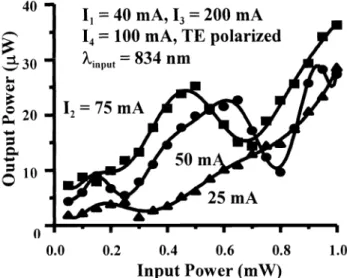
Figure 1 shows the layout of the device. The active loop of 300 im in radius is formed with a curved ridge waveguide with a ridge width of 4 m (a single-mode waveguide). The loop is coimected to an MMIWA with a length of 460 pm and a ridge width of8 rim. The MMIWA serves the function ofthe coupler with the nonlinear coupling effect. Then, the input and output legs are formed with 4 m wide SOA's. Both have the lengths of about 600 tim. The device was fabricated on a four-period GaAs/AlGaAs multiple quantum well epitaxial structure. The GaAs wells (10 nm thick) and A1025Ga075As barriers (20 nm) were sandwiched by two 140 nm thick i-Al025Ga075As separate confinement layers, and p-Al06Ga04As and n-A106Ga04As cladding layers. Electro-luminescence measurements indicated that the gain peaks in the TE and TM directions were 834 and 8 1 7 nm, respectively. The fabrication procedures were the same as the typical processes for semiconductor lasers except the etching technique for forming the ridge waveguides. To achieve vertical and smooth etched walls for reducing bending loss and to minimize surface damage, the LJVlaser-assistedcryo-etching teclmique was used. The etching depth was 1 .6 tim. For injecting different currents into different areas, we divided the electro-pad into four disconnected regions, indicated by the injection currents I (input-output region), '2(MMIWA),13 (one-quarter ofthe loop), and 14 (three-quarter ofthe loop).
In experiments, 100-fsec pulses from a mode-locked Ti:sapphire laser were first passed through a monochromator for selecting the required center wavelengths and spectral widths of input signals. With a fixed center wavelength of the fsec pulse from the laser, the allowed wavelength range for selection was about 1 0 nm. After the monochromator, the pulse of a selected wavelength had a width of about 1 .4 psec. Such signals were end-coupled into the input leg of the device. The signals emergent from the output leg were passed through another monochromator for filtering out amplified spontaneous emission noise. Figure 2 provides three sets ofdata showing power-dependent switching when the TE-polarized input signals at 834 rim (TE gain peak) were used. The horizontal axis represents the average input power before entering the input leg. The injection current values of I, 13, and 14 were fixed at 40, 200, and 100 mA, respectively. Note that this arrangement leads to the injection current density ratio of the one-quarter section over the three-quarter section of the loop to be about 6: 1 .One
can see that significant nonlinear switching occurs when '2is sufficiently large. Generally speaking, a larger '2leads
to a
smaller switching power. It is noted that the 0.6 mW switching power in the horizontal axis of Fig. 2 corresponds to a
switching energy of 79 fI if 1 % of input coupling efficiency is assumed.
To observe the cross-switching effect, we prepared two psec pulses for pump-probe experiments. Figure 3 shows a typical result of the pump-probe experiments for the probe output power level as a function of the pump-probe time delay.
Here, the pump was TM-polarized at 825 nm with the input power at 0.75mWand the probe was TE-polarized at 834 nm with the input power at 0.25 mW. The zero time delay was approximately set at the first peak of the data curve. One can see the narrow two-hump feature of about 5psecin width around the zero time delay. It is supposed to correspond to the situation that the pump and probe overlap in most part of the device. After the two-hump feature, a long tail in an oscillatory manner
can be observed. This long tail is supposed to come from the period of gain recovering from saturation in the MMIWA and loop. Its length should be in the order ofcarrier lifetime.
In interpreting the device operation with cw signals, we considered the nonlinear coupling effect in the MMIWA and the functions of the lateral field redistribution and amplification from the loop. Such considerations are still valid. However, with
pulsed signals the loop asymmetry needs to be considered. The nonlinear coupling in the MMIWA results in
power-dependent lateral field distribution. After splitting into the two counter-propagating components in the loop, they experience different gain levels and phase shifts in the asymmetric loop. Such differences combine with the nonlinear coupling effect acquired during the backward propagation in the MMIWA to give various distributions of the signal power between the input and output legs. When the pump-probe experiment is conducted, the nonlinear coupling process of the strong pump signal dominates the lateral field distribution of the probe signal in the MMIWA. Also, the asymmetric gain saturation due to the counter-propagating pump signals may enhance the asymmetric gain and phase factors for the counter-propagating probe signals.
3. ALL-SEMICONDUCTOR NONLINEAR OPTICAL LOOP MIRROR --
MODELLING
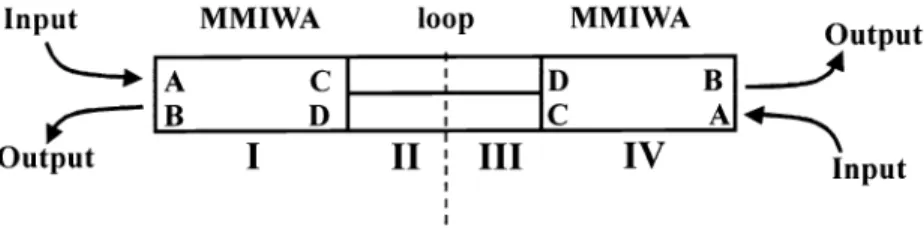
Figure 4 shows the layout of the all-SOA nonlinear optical loop device. The device consists of several parts: the loop, the MMIWA, the input port and the output port. Note that the one-quarter and three-quarter sections of the loop are divided for
different injection currents (14 and 13, respectively). The injection currents for the regions of MMIWA and input/output portion are '2 and I, respectively. All parts are made of ridge-loading waveguide SOA's. The loop with a ridge width of 4 pm
(expected to form a single-lateral-mode waveguide) is connected to the MMIWA with a ridge of 8 pm wide where two modes
can propagate. Note that in practical situations, such as in our feasibility experiment, the fabricated MMJWA may
than what is modeled here. Nevertheless, the built model should be sufficient to describe the key mechanisms of the device operation. Also, the simulation results must be helpful to device design. The input and output ports also have a ridge width of 4 im. By injecting different currents, we can control the gain factors in different parts of the device. In numerical simulation, the effective index method is used to obtain the waveguide characteristics. First, we analyze an effective slab waveguide of thickness 0.43-pm (along the transverse or x-direction) and find that only one guided mode exists in the epitaxial growth direction. Then, the lateral or y-direction guidance is provided by an effective slab waveguide of thickness equal to the ridge width. Here, the rectangular coordinates are adopted. Based on the device geometry, the signals propagate along the ridge-loading waveguides in both +z and -z directions.
We first consider the self-switching case. Figure 5 shows the typical energy-dependent switching result, describing the output pulse energy versus the input pulse energy. The solid, dashed, and dash-dotted curves represent the output pulse energies emerging from the output port, from the input port, and the sum ofthe two, respectively. Here, the small-signal gain factor G2 (= exp(gL)) of MMIWA is 4 dB (corresponding to the gain constant g = 1 842 m1), and those (G3 and G4) ofthe
three-quarter and one-quarter loop sections are 5 dB and 35 dB (corresponding to g = 810 m1 and 17011 rn), respectively. The full-width-at-half-maximum (FWHM) pulse width ofthe input pulse is set to be 2 psec.
To investigate cross-switching phenomena, we conduct pump-probe simulation. Figure 6 shows the output energies of
the probe pulse (from the output port, from the input port, and the sum from both ports) as functions of the time delay between the pump and probe. Here, the positive (negative) time delay means that the pump leads (lags) the probe. For
comparison, we also compute the light transit times in the different device segments. The transit times in the MMIWA and one-quarter loop are about 5.67 psec and 5.39 psec, respectively. The input energy ofthe pump pulse is 0.05 pJ and that of the probe pulse is 0.002 pJ. Both the pump and probe have pulse width at 2 psec. The small-signal gain factors G2, G3 and G4 are fixed at 4 dB, 5 dB and 35 dB, respectively. One can see that the curve ofprobe energy from the output port exhibits a hump around zero time delay and extends a long tail.
4. SEMICONDUCTOR LASER MODE-LOCKING --
MODELLING
To investigate the mode-locked semiconductor lasers with MMI SOA's, we need to first analyze the propagation ofan optical pulse in the key component ---the MMI SOA. We consider an SOA with a ridge-loading waveguide structure. The ridge
width is 8 ,um. Although our theoretical and numerical results are quite general for any laser epitaxial structure, the
following calculations are based on the epitaxial structure as follows. Four periods ofquantum well/barrier (10 nm GaAs for
well and 20 nm Al0 25Ga075As for barrier) are sandwiched by 200 nm thick i-Al0 25Ga0 75As separate confinement layers on
both sides to form the guiding layer of thickness 0.43 tm. The upper- and lower-cladding layers are composed of p- and n-type Al06Ga04As. We use the effective index method for calculating the effective refractive index of the waveguide. Based on the waveguide structure described above, we first analyze an effective slab waveguide of thickness 0.43 tm (along the x-direction) and find that only one guided mode exists in the epitaxial growth direction. Then the lateral or y-direction guidance
is provided by an effective slab waveguide of thickness 8 im to ensure the existence of two propagating modes in this
dimension. From this model, it is found that the effective refractive indices (relating to the field distribution in the lateral
direction, i.e., the y-axis) are n1 = 3.401 and n2 = 3.3995 in the ridge-loading region and outside, respectively.
The setup ofthe mode-locked semiconductor laser with an MMI SOA for our simulations is schematically shown in Fig. 7. The gain medium is the MMI SOA of which the length is chosen to be one coupling length. In front of it, we preparea
section of passive waveguide for trimming the lateral pattern of the input optical pulse before incidence upon the bar-port side ofthe MMI SOA. In practice, this arrangement is feasible with the quantum well intermixing technique. Three mirrors of 100% reflectivity are used to form a ring cavity so that the oscillating signal circulates through the bar-port side of the MMI
SOA. Two objective lenses are used for collimating input and output optical beams. A spatial filter is also inserted for
controlling the lateral pattern of the oscillating signal. It can block part of the bar-port optical energy by shadowing along the lateral direction an offset distance ®ofj measured
from the center (y =
0) ofthe
MMI SOA. We use the cross-port as the laser output port and extract the output pulse with a tilted mirror. The length of the ring cavity is assumed to be much longer than the light speed times the carrier lifetime, so that the MMJ SOA can recover from gain saturation when the circulated pulse reenters the MMI SOA. An isolator is used to guarantee one-way oscillation in the laser cavity. Meanwhile, we assume that both end facets of the MMI SOA are perfectly anti-reflection coated. Note that in calculating the pulse evolution, we virtually connect the output of the spatial filter to the input of the passive waveguide section, disregarding the propagationeffect (diffraction) in the cavity.
We start the simulation with a long Gaussian pulse (with FWHM pulse width z 200 psec) to see whether the pulse can be compressed. The evolution of pulse emerging from cross and bar ports of the MMI SOA (with G0 = 25 dB) is shown in Figs. 8(a) and (b), respectively. Here, the ordinate indicates the power obtained by integrating the intensity of the pulse over
the lateral dimension for each port. We can see that the pulse is gradually compressed after a few round trips. Note that the peak power of the output pulse from the cross-port is higher than that emerging from the bar port. This is similar to the result
of nonlinear coupling mode locking based on a directional coupler .The dynamic development of the compressed pulse is
also shown in Fig. 9 by plotting the evolution of the FWHM pulse width and peak position during the first twenty round trips. The asymptotically steady values of the FWHM pulse width and peak position show the strong evidences of mode-locking
feasibility.
5. CONCLUSIONS
In this paper, we have demonstrated the implementation of efficient power-dependent switching in an all-SOA nonlinear optical loop mirror. Numerical simulations showed the consistent trends. Either with cw or pulsed signal, high speed all-optical switching is feasible. Also, we illustrated the concepts of novel mode-locking schemes of semiconductor lasers based on nonlinear coupling in MMI SOAs by showing numerical simulation results.
ACKNOWLEDGEMENTS
This research was supported by National Science Council, The Republic of China, under grants NSC 87-2215-E-002-006, NSC 87-2215-E-002-007, NSC 87-2215-E-002-009, NSC 2112-M-002-004, NSC 2215-E-OO2-O2, and NSC
88-22 1 5-E-002-O 14.
REFERENCES
1. J. Cai, K. Feng, X. P. Chen, and A. E. Willner, "Equlization ofnonuniform EDFA gain using a fiber-loop mirror," IEEE Photon. Technol. Lett. vol. 9, pp. 916-918, 1997.
2. W.S. Wong, S. Namiki, M. Margalit, H. A. Haus, and P. Ippen, "Self-switching of optical pulses in
dispersion-imbalanced nonlinear loop mirrors," Opt. Lett. vol. 22, pp. 1150-1152, 1997.
3. D. Wang, E. A. Golovchenko, A. N. Pilipetskii, C. R. Menyuk, and M. F. Arend, "Nonlinear optical loop mirror based on standard communication fiber," J. Lightwave Technol. vol. 15, pp. 642-646, 1997.
4. J. P. Sokoloff, P. R. Prucnal, I. Glesk, and M. Kane, "A terahertz optical asymmetric demultiplexer (TOAD)," IEEE Photon. Technol. Lett. vol. 5, pp. 787-790, 1993.
5. M. Eiselt, W. Pieper, and H. G. Weber, "SLALOM: semiconductor laser amplifier in a ioop mirror," J. Lightwave Technol. vol. 13, pp. 2099-2112, 1995.
6. E. Jahn, N. Agrawal, W. Pieper, H. J. Ehrke, D. Franke, W. Furst and C. M. Weinert, "Monolithically integrated
nonlinear Sagnac interferometer and its application as a 20 Gbit/s all-optical demultiplexer," Electron. Letters, vol. 32, pp. 782-784, 1996.
7. J. H. Lee, D. A. Wang, H. J. Chiang, D. W. Huang, S. Gurtler, C. C. Yang, Y. W. Kiang, B. B. Chen, M. C. Shih and T. J.
Chuang, "Nonlinear switching in an all-semiconductor-optical-amplifier loop device," IEEE Photonics Tecimology
Letters, Vol. 11, pp. 236-238, 1999.
8. J. H. Lee, D. A. Wang, Y. W. Kiang, H. J. Chiang and C. C. Yang, "Nonlinear Switching Behaviors in a Compact All-Semiconductor-Optical-Amplifier Sagnac Interferometer Device," IEEE J. Quantum Electronics, Vol. 35, pp. 1469-1477,
1999.
9. H. G. Winful and D. T. Walton, "Passive mode locking through nonlinear coupling in a dual-core fiber laser," Opt. Left.,
vol. 17, pp. 1688-1690, 1992.
10. C. W. Hsu and C. C. Yang, "Passive mode locking of semiconductor lasers based on nonlinear directional coupling,"
Opt. Left., vol. 21, pp. 878-880, 1996.
1 1. S. M. Jensen, "The nonlinear coherent coupler," IEEE J. Quantum Electron., vol. 18, pp. 1580-1583, 1982.
12. 5. R. Friberg, A. M. Weiner, Y. Silberberg, B. G. Sfez and P. S. Smith, "Femtosecond switching in a dual-core-fiber nonlinear coupler," Opt. Lett., vol. 13, pp. 904-906, 1988.
C
13 14 D 12B
C MM! WA
AOutput
-
Input
Fig. 1 Layout ofthe all-SOA nonlinear optical ioop mirror.
Ii = 40 mA, 13 =
200mA
14 100 mA, TE polarized
Xinput 834 nm
'2
75 mA
40 1025 mA
o• -•
U - U I U 0.0 0.2 0.4 0.6 0.8 1.0Input Power (mW)
Fig. 2 Typical self-switching results ofthe all-SOA nonlinear optical loop mirror. 8
6
0
0 10 20 30 40 50 60 70
Time Delay (psec)
MM! WA
________
BL
Output
AI
Iv
Input
Fig. 4 Model for numerical simulations of the nonlinear optical loop mirror.
C
-0.5
20 0.5 Time (nanoseconds)
Fig. 7schematicsetup for laser mode locking. Fig. 8(a) Pulse evolution from the cross port.
Input
MMIWA loopOutput
I
C D D CII
III
5 4•\ /_•__-'
3 2 / //
1 / \,,
1.6 1.2 0.8 0 lriputPort Output Port —- — - Total 0.4 Input Port Output Port —. Total 0 0.1 0.2 0.3 0.4 0.5Input
Pulse Energy (pJ)
Fig. 5Typicalresults of self-switching simulations.
-10 0
2040 50
Time Delay (ps)
Fig. 6 Typical results of cross-switching simulations.
output M isolator 0) 0 0. M 0 Round Trips
U) .S 200 -c -o 150 C) (a a. 100
I
50 0 10 -0.5 0 Round TripsFig.8(b) Pulse evolution from the bar port
Time (nanoseconds) 250 U) C C 0 U) 0 a. (U U) a. 10 Round Trips