A Digital Golay-MPIC Time Domain Equalizer for
SC/OFDM Dual-Modes at 60 GHz Band
Wei-Chang Liu, Fu-Chun Yeh, Ting-Chen Wei, Ching-Da Chan, and Shyh-Jye Jou
Abstract—In this paper, a digital time domain equalizer (TDE) for 60 GHz radio frequency transmission systems is presented. Significantly, the TDE supports both single carrier (SC) and orthogonal frequency-division multiplexing (OFDM) operation modes for digital baseband receiver. In order to improve the performance, the proposed TDE adopts Golay sequence aided one-shot channel estimation and modified multi-path interference cancellation (MPIC) equalization. Targeting on the line-of-sight (LOS) channel characteristic, MPIC is simplified with single-tap for complexity reduction. From the area efficiency point of view, both SC and OFDM modes are designed within a single hardware to yield 99% of area sharing. The Golay-MPIC TDE structure is realized as feed-forward data path with 8X-parallelism to achieve 2.64 GS/s at 330 MHz clock rate. The Golay-MPIC TDE is fab-ricated as a part of a digital baseband with 65 nm 1P9M general purpose process. The area of Golay-MPIC TDE occupies 1.05 with 405 K gate counts. Besides, the power dissipations for SC and ODFM modes are 56.71 mW@220 MHz (1 V) and 91.29 mW@330 MHz (1.1 V), respectively. Finally, the chip can provide the maximum throughput 15.84 Gb/s (2.64 GS/s with 64-QAM modulation).
Index Terms—Dual modes, OFDM, SC, time domain equalizer, WPAN, 60 GHz, 802.15.3c.
I. INTRODUCTION
T
HE unlicensed 60 GHz radio frequency (RF) band is a new opportunity to achieve multi-gigabit transmission rate in indoor wireless transmission environment. A number of previous works in [1] and references therein presented that the 60 GHz band has the characteristics of highly directional, highly atmospheric absorption, narrow beamwidth and no rich multi-path effect. For digital home applications, the 60 GHz band transmission is adopted in three standards to reach beyond gigabit per second (Gb/s) in wireless transmission and mitigate the cable tied routing, specifically IEEE 802.15.3c wireless per-sonal area network (WPAN) [2], IEEE 802.11ad wireless local area network (WLAN) [3], and ECMA TC387 [4]. The appli-cations include high definition multimedia interface (HDMI) cable replacement, uncompressed high definition (HD) video streaming (instead of the compressed HD video stream [5]), HD audio/video source/sink and data transmission. The IEEE 802.15.3c standard provides three PHY modes including single carrier (SC), high-speed interface (HSI), and audio/visual (AV) modes. The SC PHY uses single carrier modulation whereas theManuscript received April 19, 2012; revised August 21, 2012 and November 20, 2012; accepted December 17, 2012. Date of publication March 21, 2013; date of current version September 25, 2013. This work was supported in part by National Science Council of Taiwan under Grant NSC101-2220-E-009-023, TSMC university shuttle program, National Chip Implementation Center, and MediaTek. This paper was recommended by Associate Editor B.-H. Gwee.
The authors are with the Electronics Engineering Department and Institute of Electronics, National Chiao Tung University, Hsinchu, 300 Taiwan (e-mail: [email protected]; [email protected]).
Color versions of one or more of the figures in this paper are available online at http://ieeexplore.ieee.org.
Digital Object Identifier 10.1109/TCSI.2013.2244321
HSI and AV PHYs employ orthogonal frequency-division mul-tiplexing (OFDM) modulation. In contrast, the IEEE 802.11ad standard provides two PHY modes, such as SC and OFDM. Both of the IEEE standards are proposed for the indoor wireless transmission with more than Gb/s data rate and operated at 60 GHz RF band. The experiment results [6]–[9] indicate that the multi-path effects, caused by the reflection, can be mitigated by directional antenna. Also, for 60 GHz RF band, the reflected signal has serious attenuation by wall reflection. Thus, the RMS delay spread of 60 GHz transmission is less than that of low frequency bands [7], [9]. In addition, the beamforming technique is adopted in both IEEE standards to enhance the transmission power and further realize the line-of-sight (LOS) environment.
Prior works focused on mixed-signal synchronization to sup-port high-speed operation [10]–[12]. The approaches only pro-vide simple modulation scheme up to QPSK. The feedback loop from the digital-domain to analog-domain results in system sta-bility issue. Furthermore, the error propagation problem in the subsequent decision feedback equalizer (DFE), only applicable for SC transmission, leads to performance loss. Fortunately, the main trend in modern transmission system design is digital base-band transceivers with all-digital synchronization scheme, in which no feedback loop exists from digital domain to analog domain. In general, the digital baseband contains three main blocks, which are all-digital synchronization, channel estima-tion/equalization and data demodulation. The most important part is the channel estimation/equalization. For channel equal-ization, OFDM modulation has the advantage of inter symbol interference (ISI) free property and easy equalization for fre-quency-selective channel [13] with frequency domain equal-izer (FDE). As for SC modulation, the ISI degrades the system performance and the computational complexity of time domain equalizer (TDE) is proportional to the RMS delay spread [14] of multipath fading channel.
The SC and HSI modes in IEEE 802.15.3c and the SC and OFDM modes in IEEE 802.11ad consist of the similar preamble and payload structure. Therefore, to implement an equalizer in a single hardware structure with the same estimation/equalization method to achieve the least hardware cost and maximum hard-ware sharing between SC and OFDM modes of these two stan-dards are possible. In addition, it is a great challenge to simulta-neously achieve the specified high sampling rate and maintain low hardware complexity. As a result, parallel architectures are adopted to solve the dilemmas of high sampling rate and hard-ware complexity.
Digital equalizers such as [14], [15] and [16] are proposed to eliminate the channel effects and be applicable for digital base-band. The least square (LS) and least-mean-squares (LMS) fre-quency domain equalizer in [14] has the problem of noise en-hancement in the first LS stage which will result in performance
degradation. Another concern is the performance saturation in high SNR under OFDM mode. The efficient Golay correlator adopted in [15] and [16] provides more accuracy channel es-timation as compared with LS. The Golay correlator has the same function as matched filter but with less hardware cost. However, AWGN noise influences the accuracy of the estimated channel impulse response (CIR). As a result, the performance droops while transforming from channel impulse response in time domain to channel frequency response (CFR) in frequency domain. This phenomenon impacts the performance of MMSE equalizer. In [16], the channel is estimated and equalized at the same domain. Although it performs superior performance with less hardware cost, only applicable for SC transmission and BPSK modulation is the shortcoming. In additional, the hard-ware complexity grows significantly while supporting higher QAM modulations.
The hardware complexity of linear equalizer is much more sensitive to the length of CIR spread than that of multi-path in-terference cancellation (MPIC) structure [17]. The data storage requirements and iteratively channel cancellation are the major concern of MPIC. Appreciating to the highly directional charac-teristic and/or beamforming technique, the transmission channel can be simplified as LOS. Therefore, the complexity of equal-ization in time domain can be greatly reduced from MPIC struc-ture. In summary, the design challenges of the digital equalizer for 60 GHz system are described as follows:
1) Low computational complexity algorithm of digital equal-izer for 60 GHz channel characteristics.
2) Efficient equalizer architecture for SC and OFDM dual modes.
3) Very high sampling rate and beyond Gb/s throughput rate. Considering the design issues as mentioned above, an 8X-parallelism digital TDE is proposed by using Golay sequence aided channel estimation and simplified one-tap multi-path interference cancellation (MPIC) structure for channel equalization. Since the channel estimation and equal-ization is operated in time domain, there is no performance loss induced by domain transformation. The equalization structure, simplified as one-tap delayed cancellation from original MPIC structure, reduces the large storage elements and iterative executions. That is because the size of storage elements and number of iteration are in proportional to the number of tap. With the one-tap time domain ISI cancellation by subtracting the multi-path channel response, the computational complexity is greatly reduced compared with the channel inversion and multi-tap FIR filter of conventional TDE. In contrast with the FDE, the proposed equalizer can be operated in SC and OFDM dual modes without additional hardware overhead.
The paper is organized as follows. The system specification and overview of the equalizer state-of-the-art are described in Section II. The proposed LOS Golay-MPIC TDE for SC and OFDM dual modes is presented in Section III. In addition, the detail algorithm, performance analysis and system architecture are addressed. The comparisons of the digital equalizers for 60 GHz band are described in Section IV with measurement results. Finally, the conclusions are given in Section V.
II. SYSTEMSPECIFICATIONS
Although there are many methods to achieve the target of data rate beyond Gb/s in wireless communication, for example using high-order modulation scheme or multi-input and multi-output (MIMO) system [18], raising the sampling rate is the most direct
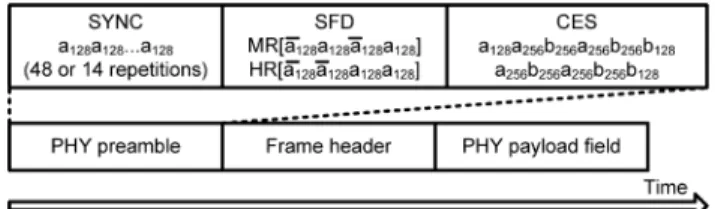
Fig. 1. PHY frame format.
way since the data rate is proportional to the sampling rate. The crucial is the usage of 60 GHz RF band, which provides large bandwidth and makes the ultra-high sampling rate to be avail-able. With a moderate modulation scheme, the data rate could be multiple times of the sampling rate. In this way, it is easier to achieve the target beyond Gb/s data rate.
A. SC and OFDM Mode Specifications of 802.15.3c
In this paper, the IEEE 802.15.3c standard is adopted as the equalizer design example because it is the first IEEE wireless standard to reach data rate beyond 1 Gb/s. The SC modulation offers lower complexity and low power operation, whereas the OFDM modulation has high spectral efficiency. Also, different data modulation schemes are provided to achieve specified data rate for different usage models [19]. The frame structure and PHY preamble of both SC and OFDM modes are specified as shown in Fig. 1. The frame synchronization (SYNC) and start frame delimiter (SFD) fields are used to carry out the frame de-tection and frame timing estimation, respectively. The channel estimation sequence (CES) field, which is composed of the spec-ified complementally Golay sequences, is employed to perform channel estimation. The channel model is based on the golden sets released by IEEE 802.15 TG3c group [20]. The test channel is LOS channel model with RMS delay of 3.2 ns from [20]. The channel model contains two conspicuous tones, such as main path and reflected path with delay. In this paper, the design target is the realization of the equalizer for both SC and OFDM (HSI) modes of 802.15.3c within the same hardware because of the similarity of frame structure.
B. Comparison of Time and Frequency Domain Equalizer
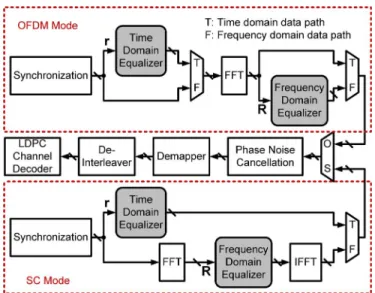
From the hardware efficiency point of view, the equalizer hardware has to be designed to operate in both SC and OFDM modes. For the purpose to operate SC and OFDM modes within a single hardware, the equalizer must adopt the same structure for both modes. Fig. 2 illustrates the block diagram and data path for FDE and TDE in digital baseband receiver architecture of SC and OFDM modes.
The FDE for SC mode requires a pair of FFT and IFFT to transform data to frequency domain for equalization and back to time domain for data demodulation, respectively. In contrast, the FDE for OFDM mode inherently requires single FFT. As a result, the total computational overhead of FDE between SC and OFDM modes is an IFFT. Research shows that when the RMS delay spread increases to certain length, the SC-FDE has less computational complexity than the SC-TDE [21]. With the aid of cyclic prefix (CP), the SC-FDE can be implemented easily than ever before [22], [23].
The TDE requires a channel matrix inversion for coefficient update and a FIR filter for channel equalization. The computa-tional complexity of TDE is proporcomputa-tional to the length of the filter taps determined by the length of CIR. However, the supe-riority of TDE is no overhead for both SC and OFDM modes.
Fig. 2. Block diagram and data path for time and frequency domain equalizers.
In summary, FDE has fixed single-tap and less computational complexity than TDE for long CIR. The drawback is that addi-tional CP reduces the data rate. For a long CIR, the CP period has to be increased to prevent the ISI effect and maintain the cir-cular convolution property. On the other hand, the conventional TDE does not need CP added transmission, but it suffers from large computational complexity in the hardware implementa-tion.
Previous works focused on FDE structures, [14] and [15], be-cause of the fixed computational complexity. According to the high propagation attenuation and small multi-path effect of 60 GHz band environments as referred in Section I, the channel characteristics are also different from the traditional lower fre-quency bands. As [1], [6], [19], and [24] indicate, with the di-rectional antennas, the channel response can be modeled as LOS situation with two paths. Besides, the second path of reflection contains much lower gain. By inspecting the channel convolu-tion, the channel de-convolution can be simplified as a delayed cancellation. Therefore, for TDE, the matrix inversion proce-dure is possibly ignored and then the FIR filter can be shortened as single-tap substraction, which will be described in Section III.
C. Hardware Design Considerations
The sampling rate is specified as 1760 MHz in SC mode and 2640 MHz in OFDM mode. Therefore, the clock rate in the hardware design has to be able to operate at 2640 MHz for SC and OFDM dual modes system. There are two ways to fulfill the requirement, such as pipelined and parallel structures. Con-sidering a system with high clock rate, long computation path and loop within the path, a deep pipelined structure is not an appropriate solution, because of the overhead of large flip-flops insertion and the extra loop delay. On the other hand, the parallel structure can be employed to reduce the clock rate and maintain the throughput at the same time. The drawback is that the area is proportional to the number of the parallelism. Fortunately, the size of memory, which occupies the large portion of area, is not increased with the number of parallelism.
In this paper, a combined parallel and pipelined structure is presented based on the following points of view. Considering the operation speed limitations of the digital and standard cells, the baseband structure is designed at 330 MHz with 8X-paral-lelism. Then, the data path of TDE is fulfilled as feed-forward to eliminate the feedback loop. Therefore, pipeline stages can be
TABLE I
SYSTEMPARAMETERS OFSC/OFDM MODE
Based on the proposed 8X-parallelism structure.
easily inserted to satisfy the required operation clock without performance loss and stability issue caused by long feedback delay. In summary, the system parameters are listed in Table I.
III. LOS GOLAY-MPIC TIMEDOMAINEQUALIZER
In order to obtain the accurate channel estimation and reduce the hardware complexity, the combined architecture of Golay sequence aided channel estimation and simplified multi-path in-terference cancellation (MPIC) equalization is proposed to re-alize the TDE in SC and OFDM dual modes of 60 GHz systems. Comparing to the Golay sequence aided time domain channel estimation with frequency domain equalization method as pro-posed in [15] and [25], no additional IFFT is required.
A. Golay-Sequence Aided Channel Estimation
Golay sequences with length are generated by delay and weight vectors with of each length and a recursive algorithm [26], [27]. Golay sequences are complementary sequences, which have an attractive property that the sum of their autocor-relations has single maximum peak without side lobe.
A pair of Golay sequences and of length , where is a power of 2, has the following autocorrelation property
(1) where
(2) and
(3) Both CES and PCES fields as shown in Fig. 3 are constructed by Golay sequences and can be divided into two parts, “Part a” and “Part b.” The CES has a regular configuration, namely, repetitions of base sequences with length and cyclic prefix and postfix with length . The base sequences for “Part a” and “Part b” are Golay sequences and . Then, the total
Fig. 3. Golay sequences of CES and PCES field.
and are and , and are and
, where is 256 and is 2.
The received sample in CES field can be expressed as
(4) where is the channel estimation sequence as shown in Fig. 3, h is the time domain CIR, is the length of CIR and
is the AWGN noise.
The Golay correlator is used to calculate the correlation values and between the received CES and Golay sequences. Therefore, and can be expressed as
(5) (6) After removing the CP from the correlation values, the cor-relation values are aligned to the beginning of each Golay se-quences and described as
(7) (8) Furthermore, the estimated channel can be acquired as
(9) Therefore, with system specified parameters, the equation can be expressed as
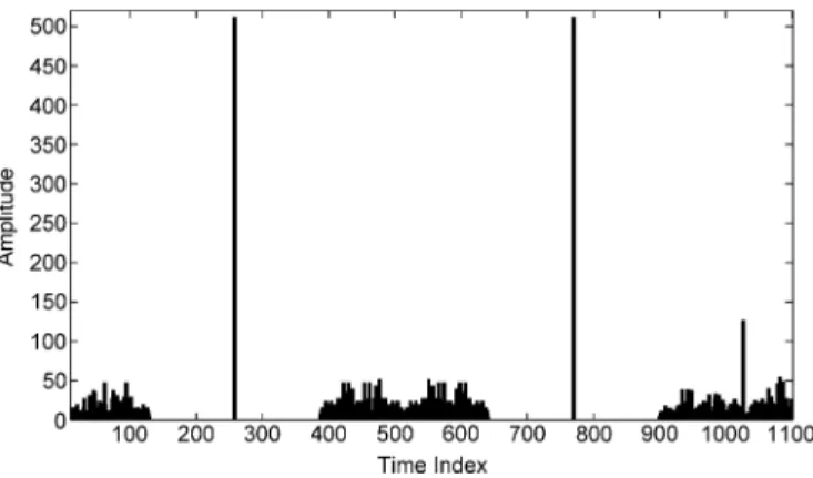
(10) The correlation result of specified Golay sequence is shown in Fig. 4. Obviously, there are two zero-correlation zones with the length of 128 before and after the main peak. Therefore, the channel impulse spread has to be restricted within these zones. Otherwise, CIR spread will ruin the orthogonality and induce performance loss. In order to conquer the pre-cursor ISI in non-line-of-sight (NLOS) channel, and pair, which has additional pre-zero-correlation zone compared with the au-tocorrelation results of in [1], is used. Finally, the noiseless CIR is employed to perform MPIC equalization.
B. Multi-Path Interference Cancellation Equalization
MPIC method is an efficient way to suppress inter-path interference [28]. Actually, MPIC is composed of two parts.
Fig. 4. Correlation result of Golay sequence.
The first part is multi-path interference replica, and the second part is multi-path interference cancellation [17], [29]. The original MPIC algorithm iteratively executes path inter-ference cancellation, which consumes lots of execution time (without loop unrolling) or leads to large latency and hardware complexity (with loop unrolling). In this system, the iteration number can be simplified as one due to the LOS channel characteristics. The cancellation is also modified using delayed cancellation to reduce the storage elements. As a result, the hardware complexity can be greatly reduced.
As mentioned in Section II, the LOS channel has only two dominant paths. Therefore, the received sample of is ex-pressed as
(11) where is the transmitted data and is the time index of second path.
A modified MPIC from [17] has two stages, such as initial acquisition and updating stages. In initial acquisition stage, the CIR is obtained from channel estimation. The , which is defined as the initial data, can be derived as
(12) In the following updating stage, the interference in received signal is canceled by subtracting the second path and then the result is divided by the main path gain to get the updated trans-mitted data .
(13) Without loss of generality, (13) can be simplified as
(14) By expanding and , and ignoring the noise term, (14) can be rewritten as
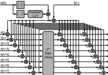
Fig. 5. Block diagram of the proposed Golay-MPIC TDE.
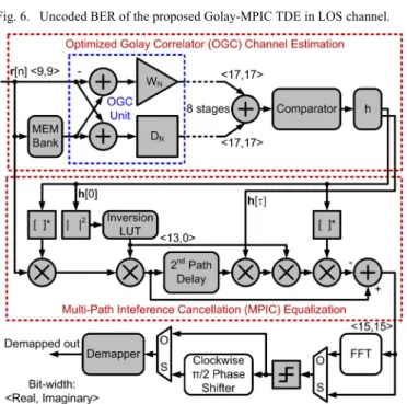
Fig. 6. Uncoded BER of the proposed Golay-MPIC TDE in LOS channel.
Fig. 7. Detail architecture of the proposed Golay-MPIC TDE.
Obviously, the term of can be neglected since the multi-path gain is small enough to make close to zero. Therefore, is approximated to .
In conclusion, only the 2nd dominant path should be con-sidered since the path interferes the received signal. By using simplified MPIC method, the hardware complexity is reduced compared with conventional TDE. The required tap number is the multi-path number instead of proportional to the length of CIR. In this system, the tap number is one for LOS channel of 60 GHz. For NLOS channel condition, the simplified MPIC re-quires multiple taps to suppress the inter-path interference. Fur-thermore, comparing to the conventional FIR filter, the MPIC method requires one multiplication, one substraction and one division for each symbol instead of multiplications and additions regardless of the computational complexity for matrix inversion operation.
C. Block Diagram and Data Flow
The block diagram of the proposed Golay-MPIC TDE for SC and OFDM dual modes is shown in Fig. 5, and the pseudo-code of the system flow is shown as below
IF (received signals==CES of preamble or PCES) THEN Do the one-shot Golay sequences aided channel estimation to evaluate the channel impulse response. ELSE IF (received signals==payload data)
Equalize the received data by MPIC TDE. CASE modulation mode OF
SC:
Send equalized signal to demapper. OFDM:
Transform the equalized signal to frequency domain by FFT.
Send frequency domain data to demapper. ENDCASE
ELSE Sleep. END IF
The proposed Golay-MPIC TDE first estimates the CIR during the CES field by Golay sequence aided channel esti-mation. After the CIR is obtained, the values and indexes of the maximum two impulses are sent to MPIC block. While the payload field, the MPIC subtracts the second path for inter-ference cancellation. In each PCES field, the CIR is updated by Golay-MPIC TDE again based on Golay sequence aided channel estimation.
D. Performance Simulation and Analysis
The performance simulation of the proposed Golay-MPIC TDE in LOS channel is shown in Fig. 6. The performance requirement of coded BER is , specified in 802.15.3c with QPSK modulation for SC and QPSK modulation for OFDM. According to the channel decoder implementation, the BER before channel decoded is set as . With QPSK modulation in SC mode, the proposed Golay-MPIC TDE achieves the BER at SNR of 8 dB. With QPSK modula-tion in OFDM mode, SNR at BER is 6 dB. Apparently, the performance of OFDM (HSI) mode is better than SC mode, because the FFT has the effect of smoothing noise.
E. Architecture Design
The system architecture of the proposed Golay-MPIC TDE is illustrated in Fig. 7. The signal flow of SC mode is almost the same as that of OFDM mode. Only additional “Clockwise Phase Shifter” is used in SC mode since the modulation in SC mode is M-PSK.
In channel estimation, the optimized Golay correlator (OGC) [30] architecture is adopted to implement the Golay sequence aided channel estimation. Compared with the efficient Golay correlator employed in [15] and [16], OCG has less computa-tional complexity while maintaining the same performance [31]. By using the characteristic of Golay sequence, the OGC is able to realize the same function as matched filter with less hardware cost. The number of stages for OGC is equivalent to ,
Fig. 8. Complexity improvement of (a) multiplication number of OGC, (b) ad-dition number of OGC, and (c) tap number of equalizer of the proposed Golay-MPIC TDE.
where is the length of specified Golay sequence 256. There-fore, there is 8-stage of OGC unit to perform the channel esti-mation. In hardware implementation, the multiplier “ ” can be simplified as bypass circuit or an inverter with the pre-de-fined Golay sequence. In addition to fulfill the requirement of OGC input, a length of 256 FIFO is implemented by two single port memory blocks from shared memory bank, with interleaved read and write accesses. The with the 256 samples delay and are concurrently sent to the OGC. The delay element “ ” in each OGC stage has the length of (128, 64, 32, 16, 8, 4, 2, and 1 for stage 7, 6, 5, 4, 3, 2, 1, and 0, respectively). During the CES and PCES fields, the CIR is acquired by the OGC channel estimation and then the indexes and values of two maximum estimated impulse responses are stored in register “h” as shown in Fig. 7. After the channel estimation procedure, the OGC channel estimation is shut down for power saving and the memory is released to other modules. As shown in Fig. 8, the OGC architecture can yield the reduction of multiplications and additions in 98.44% and 98.24%, respectively, as compared with straightforward matched filter approach.
By multiplying the conjugate of in (14), the denominator becomes a real number instead of complex number as following:
(16) It is clear that, the complex division in (14) is simplified as real division and complex multiplication. According to the pre-defined inversion look-up table (LUT), the real division can be implemented by a multiplier. The MPIC equalization as il-lustrated in Fig. 7 is employed to implement the (16). The “2nd Path Delay” block is a configurable delay-line to realize the delay.
According to the fixed-point analysis, the real- and imagi-nary-part of equalizer inputs are 9-bit. Therefore, the output of OGC is 18-bit after 9 additions. As a result, the memory size
is bits for 8X-parallesim.
Then the input of absolute power circuit just takes the MSB 9-bit of OCG output and the output of absolute power circuit pre-serves 15-bit as the input of inversion LUT. The inversion LUT is pre-defined with the approximated resolution to reduce the table size and the output is 13-bit. Finally, the equalizer output is 15-bit for both real and imaginary parts.
The proposed equalizer is feed-forward architecture without feedback loop. Therefore, no additional memory is required to
Fig. 9. Hardware reduction of the proposed Golay-MPIC TDE.
Fig. 10. 8X-parallelism architecture of OGC channel estimation.
store the received data and it has more stable performance com-pared with using DFE. The memory is used as a FIFO, with length of 256, for channel estimation. The maximum size of the second path delay-line in MPIC block is 128 determined by the length of post zero-correlation zone.
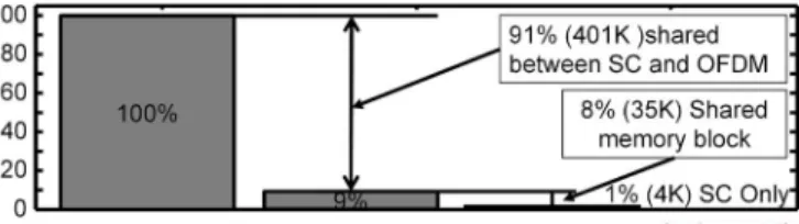
The hardware reduction of proposed Golay-MPIC TDE is shown in Fig. 9. The hardware sharing parts excluding “Clock-wise Phase Shifter” can obtain 99% hardware reduction. The gray parts as illustrated in Fig. 7 are jointing used in both SC and OFDM modes. The MEM Bank in OGC channel esti-mation is shared with the shared memory block in the baseband receiver. The FFT is not an overhead for the system since the FFT is employed to OFDM mode.
F. Architecture Parallelism Design and Synthesis Results
The 8X-parallelism architecture of OGC channel estimation is illustrated in Fig. 10. The “32D” and “1D” represent 32- and 1-sample delay, respectively. Due to processing 8 data at the same time, the arithmatic units are duplicated by 8 times and the length of delay elements are reduced 8 times. As a result, from stage 2 to stage 0, the delay elements are 1/2, 1/4, and 1/8, respectively. The non-integer delay elements can be imple-mented with the red wire routing as shown in Fig. 10. For stage 2, the bottom 4 OGC units have 1-sample delay used to realize 4-sample delay. For stage 1 and 0, the bottom 2 and last OGC units employ 1-sample delay to realize these delays.
Fig. 11. 8X-parallelism architecture of MPIC equalization.
Fig. 12. Area and power breakdown of the proposed Golay-MPIC TDE. TABLE II
GOLAY-MPIC TDEFORSCANDOFDM MODESYNTHESISRESULT
The result is synthesized with baseband receiver and excludes the memory bank shared from the shared memory block.
The 8X-parallelism architecture of MPIC equalization is illustrated in Fig. 11. As shown in (16), is a common term and can be calculated during the channel esti-mation period. After the channel estiesti-mation, the and are two fixed parameters. Therefore, the MPIC only requires a single hardware instead of 8 duplicates for the common term. The “2nd Path Delay” block is implemented with 8X-paral-lelism FIFO with 17 samples delay-line and switchs. According to the value of , the switch selects the corresponding delay data for output.
Synthesis result (together with digital baseband receiver chip) shows the proposed Golay-MPIC TDE can achieve maximum 413 MHz operating clock rate (required clock rate is 330 MHz) by using 65 nm 1P9M CMOS general purpose process. The area of Golay-MPIC TDE is about 584K (405 K gate count) and the power consumption is 120.88 mW as shown in Table II. Fur-thermore, The area and power breakdown of proposed Golay-MPIC TDE is illustrated in Fig. 12. The OGC channel estima-tion, the MPIC equalization and the rests occupy 37%, 62%, and 1% of area, respectively. Besides, the one-shot OGC channel es-timation is shut down after CIR eses-timation and then takes less than 1% of the working power. The MPIC equalization executes in each cycle and takes most of the power consumption.
Fig. 13. Performance comparison of SC mode, with QPSK modulation in LOS channel.
Fig. 14. Performance comparison of OFDM (HSI) mode, with QPSK modula-tion in LOS channel.
G. Comparison of Performance Simulation
The performance comparisons of different estimation and equalization algorithms in LOS channel are illustrated in Figs. 13 and 14. The performance comparison of SC and OFDM modes are with the modulation schemes QPSK and QPSK, respectively. The LS-LMS FDE [14], where is the least-square algorithm for channel estimation and the least-mean square algorithm for channel tracking. The time do-main Golay correlator based channel estimation with frequency domain minimum mean-square error (MMSE) equalization (Golay-MMSE) [15] is also illustrated in Figs. 13 and 14. The Golay-MMSE transforms the estimated CIR in time domain to CFR in the frequency domain and induces the MMSE equalization to eliminate the noise effect to enhance the system performance. The ideal curve, obtained by the de-convolution between the ideal CIR and received signal, is used to be a performance reference.
It is clear that the proposed Golay-MPIC TDE has quite the same performance with the ideal case in both SC and OFDM modes. The LS-LMS FDE in SC mode has better performance than that of OFDM mode as expected in [32]. However, the LS channel estimation inherently has the noise enhancement problem. As a result, the initial errors are passed to the suc-ceeding LMS tracking stage, and degrade system performance. Besides, a very small inaccuracy in CIR leads to serious CFR damage after transform the CIR to CFR. Therefore, the Golay-MMSE suffers the performance loss in this situation and has about 1.5 dB to 2 dB performance lost compared with the ideal case. The performance after channel decoding with coding rate 1/2 (762,336) shown that the proposed Golay-MPIC can achieve
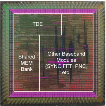
Fig. 15. Fabricated die and layout photo of Golay-MPIC TDE.
the required BER below 4 dB in SC mode and 2 dB in OFDM mode.
IV. IMPLEMENTATION ANDMEASUREMENTRESULT
The proposed Golay-MPIC TDE structure is fabricated with standard cell-based design flow using 65 nm 1P9M general pur-pose process. The design was taped out as a part of the digital baseband receiver, including all-digital synchronization, FFT, phase noise cancellation (PNC), data demodulation and shared memory bank. The structure of digital baseband receiver is de-signed as 8X-parallesim with feed-forward data path. The pro-posed Golay-MPIC TDE not only estimates the CIR and equal-izes the channel effect, but also perform the fine-boundary de-tection using the OGC output with the characteristic of Golay sequences. The TDE also removes the common phase rotation, which cannot be eliminated by time domain carrier frequency offset (CFO) de-rotator.
The die and layout photos of digital baseband receiver are shown in Fig. 15. The TDE is located in the upper-left corner. The phase de-rotator module of CFO compensation is placed in the right hand side and sends the phase de-rotated signals to the TDE. The shared memory bank is located in the lower left-corner near the TDE for the purpose of memory sharing. The TDE output goes through the center of the chip to PNC and data demodulation. Considering the restriction of area and pad number, in the fabricated chip, the demapper is for QPSK and QPSK for SC and OFDM modes, respectively. Thus, the output of demapper takes 16 pins (2 8) instead of 48 pins (6-bit for 64-QAM with 8X-parallelism).
The area of Golay-MPIC TDE is about 1.05 . The chip functionality is verified by Agilent 93000 SOC Series Test System, provided by National Chip Implementation Center (CIC). The measurement result shows that the proposed base-band receiver design can operate at the clock rate 220 MHz@1 V for SC mode and 330 [email protected] V for OFDM (HSI) mode. The power consumptions for SC and OFDM modes are 56.71 mW and 91.29 mW, respectively. With 16-QAM demodulation,
the data rate of SC mode can reach 7.04 Gb/s. Furthermore, the data rate of OFDM mode can achieve 15.84 Gb/s with 64-QAM demodulation.
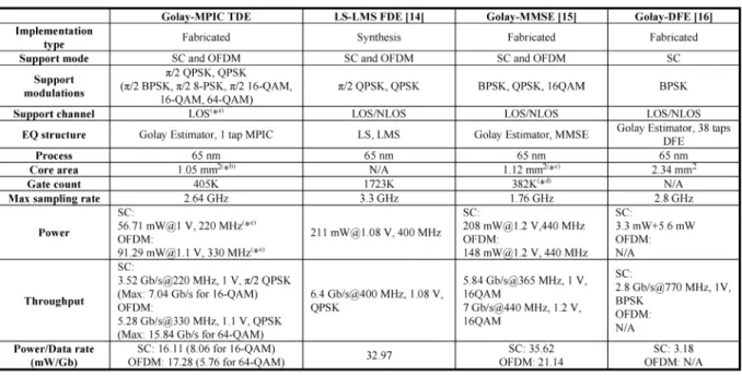
The performances of several digital equalizers of 60 GHz band are illustrated in Table III. Comparing to the other de-signs, the proposed Golay-MPIC TDE can fully support the modulation schemes of 802.15.3c standard. The LS-LMS FDE [14], Golay-MMSE [15] and Golay-DFE [16] can provide QPSK modulation, 16-QAM and BPSK, respectively. For the Golay-DFE [16], the hardware complexity will significantly increase while supporting high-order QAM modulations. Be-sides, the Golay-DFE only supports the SC transmission.
The structure of the proposed Golay-MPIC TDE has no stability issue while LS-LMS FDE and Golay-DFE have the problem of error propagation. The LS-LMS FDE and Golay-MMSE require additional IFFT for SC mode to trans-form the equalized data in the frequency domain back to time domain. For LS-LMS FDE, another additional FFT is required to transform the error estimated by LMS tracking to frequency domain. In contrast, the proposed Golay-MPIC TDE does not need the additional FFT or IFFT for supporting both SC and OFDM modes.
Considering the large attenuation caused by atmospheric ab-sorption and reflection, either the multi-antenna beamforming or the single directional antenna is more practicable than the single Omni antenna in 60 GHz environment. From the RF frond-end point of view, a multi-antenna scheme intuitively in-creases the number of antenna and mixer. On the other hand, from the aspect of transmitter and receiver, the complexity of PAs and ADCs, which are the most challenging modules, can be relaxed by taking the advantage of beamforming. The mul-tipath delay spread is also significantly shortened by using the beamforming technique [1]. Since the Omni antenna apparently requires more taps and more complex ADC and PA, the overall system overhead is significant. As a result, a single directional antenna or a multi-antenna beamforming LOS system still has less hardware cost as compared with that of the NLOS system with Omni antenna. Moreover, the multi-antenna beamforming overhead can be neglected because it is specified in the stan-dards.
Although this proposed Golay-MPIC TDE is implemented for QPSK due to the shuttle area limitation, the measurement result shows the design is able to achieve the required sam-pling rate, 1.76 GHz for SC and 2.64 GHz for OFDM, as spec-ified in IEEE 802.15.3c. The gate count of 8X-parallism archi-tecture has a little larger than 4X-parallel Golay-MMSE but it has the potential to achieve higher sampling rate. From the power dissipation point of view, the measured power dissipa-tion of proposed Golay-MPIC TDE is superior to LS-LMS FDE and Golay-MMSE for LOS channel case. Cascading with the full mode demapper, the proposed Golay-MPIC TDE is able to achieve the maximum throughput 7.04 Gb/s and 15.84 Gb/s for SC mode with 16-QAM and OFDM mode with 64 QAM mod-ulation, respectively. The power over throughput is illustrated in the table. In summary, the proposed Golay-MPIC TDE sup-ports full modulation modes in 802.15.3c standard, achieves the maximum data rate of 15.84 Gb/s.
V. CONCLUSION
In this paper, a cost efficient digital equalizer is proposed for digital baseband of 60 GHz RF systems. The low com-plexity with high accuracy Golay-MPIC TDE is designed for LOS channel (which is the quite common channel situation in 60
TABLE III
CHIPMEASUREMENTCOMPARISON
: Able to support NLOS channel with extension of the taps of MPIC. : Proportional to the chip area breakdown with core area.
: Including test circuits and FFT/IFFT. : Including an additional IFFT.
: Proportional to the chip power breakdown.
GHz band transmission). The design is examined using the spec-ification of IEEE 802.15.3c. The proposed Golay-MPIC TDE employs Golay sequence aided channel estimation with sim-plified MPIC equalization. The MPIC algorithm is modified as single-tap to reduce the computational complexity for the pur-pose to replace the conventional TDE.
From the hardware design point of view, the proposed LOS Golay-MPIC TDE equalizer is fulfilled to operate between SC and OFDM dual modes with 99% hardware sharing. In order to achieve the target of 2.64 GS/s symbol rate, the architecture is realized as feed-forward data path, for easily pipeline insertion, with 8X-parallelism.
The performance simulation indicates that the proposed Golay-MPIC TDE has superior performance in LOS channel compared with other FDE methods at 60 GHz band. The Golay-MPIC TDE can reach the required coded BER of below 4 dB in SC mode and 2 dB in OFDM mode.
Finally, the design is fabricated as a part of digital baseband receiver. The fabricated area of proposed Golay-MPIC TDE is 1.05 . The measured power dissipations at SC and OFDM modes are 56.71 mW@220 MHz (1 V) and 91.29 mW@330 MHz (1.1 V), respectively. The maximum throughput can achieve 15.84 Gb/s (2.64 GS/s with 64-QAM modulation).
REFERENCES
[1] S.-K. Yong, P. Xia, and A. Valdes-Garcia, 60 GHz Technology for Gb/s
WLAN and WPAN. Chichester, U.K.: Wiley, 2011.
[2] Wireless Medium Access Control (MAC) and Physical Layer (PHY)
Specifications for High Rate Wireless Personal Area Networks (WPANs) Amendment 2: Millimeter-Wave-Based Alternative Physical Layer Extension, IEEE Std. 802.15.3c, Oct. 2009, Part 15.3.
[3] Wireless LAN Medium Access Control (MAC) and Physical Layer
(PHY) Specifications—Amendment 3: Enhancements for Very High Throughput in the 60 GHz Band, IEEE Std. P802.11.ad/D4.1, Sep.
2011.
[4] High Rate 60 GHz PHY, MAC and PALs, ECMA-387, ECMA Int., Dec. 2010 [Online]. Available: http://www.ecma-international.org/publica-tions/files/ECMA-ST/ECMA-387.pdf, 2nd ed., , 2nd ed. , Dec. 2010 [5] R. Krishnamoorthy, “High definition, anywhere: How ultra wideband
makes wireless HDMI possible,” in Proc. IEEE Consum. Commun.
Netw. Conf. (CCNC), Jan. 2007, pp. 395–399.
[6] A. Maltsev, R. Maslennikov, A. Sevastyanov, A. Lomayev, A. Khoryaev, A. Davydov, and V. Ssorin, “Characteristics of indoor millimeter-wave channel at 60 GHz in application to perspective WLAN system,” in Proc. 4th Eur. Conf. Antennas Propag. (EuCAP), Apr. 2010, pp. 1–5.
[7] C. R. Anderson and T. S. Rappaport, “In-building wideband parti-tion loss measurements at 2.5 and 60 GHz,” IEEE Trans. Wireless
Commun., vol. 3, pp. 922–928, May 2004.
[8] X. Hao, V. Kukshya, and T. S. Rappaport, “Spatial and temporal char-acteristics of 60-GHz indoor channels,” IEEE J. Sel. Areas Commun., vol. 20, pp. 620–630, Apr. 2002.
[9] M. S. Choi, G. Grosskopf, and D. Rohde, “Statistical characteristics of 60 GHz wideband indoor propagation channel,” in Proc. IEEE 16th
Int. Symp. Personal, Indoor, Mobile Radio Commun. (PIMRC), Sep.
2005, pp. 599–603.
[10] C. Thakkar, L. K. Kong, K. Jung, A. Frappe, and E. Alon, “A 10 Gb/s 45 mW adaptive 60 GHz baseband in 65 nm CMOS,” in Proc. Symp.
VLSI Circuits (VLSIC), Jun. 2011, pp. 24–25.
[11] C. Marcu, D. Chowdhury, C. Thakkar, J. D. Park, L. K. Kong, M. Tabesh, Y. Wang, B. Afshar, A. Gupta, A. Arbabian, S. Gambini, R. Zamani, E. Alon, and A. M. Niknejad, “A 90 nm CMOS low-power 60 GHz transceiver with integrated baseband circuitry,” IEEE J.
Solid-State Circuits, vol. 44, pp. 3434–3447, Dec. 2009.
[12] D. A. Sobel and R. W. Brodersen, “A 1 Gb/s mixed-signal baseband analog front-end for a 60 GHz wireless receiver,” IEEE J. Solid-State
Circuits, vol. 44, pp. 1281–1289, Apr. 2009.
[13] J. Bingham, “Multicarrier modulation for data transmission: An idea whose time has come,” IEEE Commun. Mag., vol. 28, pp. 5–14, May 1990.
[14] F. C. Yeh, T. Y. Liu, T. C. Wei, W. C. Liu, and S. J. Jou, “A SC/OFDM dual mode frequency-domain equalizer for 60 GHz multi-Gb/s wireless transmission,” in Proc. Int. Symp. VLSI Design, Autom., Test
(VLSI-DAT), Apr. 2011, pp. 1–4.
[15] F. Hsiao, A. Tang, D. Yang, M. Pham, and M.-C. F. Chang, “A 7 Gb/s SC-FDE/OFDM MMSE equalizer for 60 GHz wireless communica-tions,” in Proc. IEEE Asian Solid State Circuits Conf. (A-SSCC), Nov. 2011, pp. 293–296.
[16] J. H. Park, B. Richards, and B. Nikolic, “A 2 Gb/s 5.6 mW digital LOS/ NLOS equalizer for the 60 GHz band,” IEEE J. Solid-State Circuits, vol. 46, pp. 5424–5234, Nov. 2011.
[17] H. Y. Chen, M. L. Ku, S. J. Jou, and C. C. Huang, “A robust channel estimator for high-mobility STBC-OFDM systems,” IEEE Trans.
Cir-cuits Syst. I, Reg. Papers, vol. 57, pp. 925–936, Apr. 2010.
[18] J. Coon, S. Armour, M. Beach, and J. McGeehan, “Adaptive frequency-domain equalization for single-carrier MIMO systems,” in Proc. IEEE
Int. Conf. Commun., Jun. 2004, vol. 4, pp. 2487–2491.
[19] T. Baykas, C. S. Sum, Z. Lan, J. Wang, M. A. Rahman, H. Harada, and S. K. Kato, “IEEE 802.15.3c: The first IEEE wireless standard for data rates over 1 Gb/s,” IEEE Commun. Mag., vol. 49, pp. 114–121, Jul. 2011.
[20] IEEE 802.15 WPAN Millimeter Wave Alternative PHY Task Group 3c (TG3c) channel-model-matlab-code-release.zip [Online]. Available: http://www.ieee802.org/15/pub/TG3c_contributions.html
[21] D. Falconer, S. L. Ariyavisitakul, A. Benyamin-Seeyar, and B. Eidson, “Frequency domain equalization for single-carrier broadband wireless systems,” IEEE Commun. Mag., vol. 40, pp. 58–66, Apr. 2002. [22] B. Farhang-Boroujeny and K. S. Chan, “Analysis of the
frequency-domain block LMS algorithm,” IEEE Trans. Signal Process., vol. 48, pp. 2332–2342, Aug. 2000.
[23] B. Rafaely and S. J. Elliot, “A computationally efficient frequency-domain LMS algorithm with constraints on the adaptive filter,” IEEE
Trans. Signal Process., vol. 48, pp. 1649–1655, Jun. 2000.
[24] Q. Nan, C. M. Robert, S. T. Shaomin, and T. Kazuaki, “60-GHz Mil-limeter-wave radio: Principle, technology, and new results,” EURASIP
J. Wireless Commun. Netw., vol. 2007, pp. 1–8, 2007.
[25] R. Kimura, R. Funada, Y. Nishiguchi, M. Lei, T. Baykas, C. S. Sum, J. Wang, A. Rahman, Y. Shoji, H. Harada, and S. Kato, “Golay sequence aided channel estimation for millimeter-wave WPAN systems,” in
Proc. IEEE 19th Int. Symp. Personal, Indoor, Mobile Radio Commun. (PIMRC), Sep. 2008, pp. 1–5.
[26] S. Z. Budisin, “Efficient pulse compressor for Golay complementary sequences,” IEE Electron. Lett., vol. 27, pp. 219–220, Jan. 1991. [27] B. M. Popovic, “Efficient Golay correlator,” IEE Electron. Lett., vol.
35, pp. 1427–1428, Aug. 1999.
[28] M. L. Ku and C. C. Huang, “A refined channel estimation method for STBC/OFDM systems in high-mobility wireless channels,” IEEE
Trans. Wireless Commun., vol. 7, pp. 4312–4320, Nov. 2008.
[29] Z. Gao, Q. Wu, and J. Wang, “A novel combination algorithm based on chip equalizer and multi-path interference cancellation,” in Proc. 7th
Int. Conf. Signal Process. (ICSP), Aug. 2004, vol. 2, pp. 1786–1789.
[30] M. Funes, P. Donato, M. Hadad, and D. Carrica, “Improved hardware implementation of a complementary sequences generator and corre-lator,” in Proc. Argentine School Micro-Nanoelectron., Technol., Appl.
(EAMTA’08), pp. 33–37.
[31] P. G. Donato, M. A. Funes, M. N. Hadad, and D. O. Carrica, “Op-timised Golay correlator,” IEE Electron. Lett., vol. 45, pp. 380–381, Mar. 2009.
[32] H. Sari, G. Karam, and I. Jeanclaude, “Transmission technique for dig-ital terrestrial TV broadcasting,” IEEE Commun. Mag., vol. 33, pp. 100–109, Feb. 1995.
Wei-Chang Liu received the B.S. degree in elec-tronics engineering from the National Central University, Jhongli, Taiwan, in 2004, and the M.S. degree from the Electronics Engineering Department and Institute of Electronics, National Chiao Tung University, Hsinchu, Taiwan in 2006. He is currently working toward the Ph.D. degree in the Electronics Engineering Department and Institute of Electronics, National Chiao Tung University.
His general research interests include VLSI implementation of digital communication baseband receiver, low power design, and timing error resilient circuit.
Fu-Chun Yeh received the B.S. and M.S. degrees from National Chiao Tung University, Hsinchu, Taiwan, in 2009 and 2011, respectively, both in electronics engineering.
He is currently an engineer in multimedia chip de-velopment department of MediaTek.
Ting-Chen Wei received the B.S. and M.S. degree in electrical engineering from National Central University, Taiwan, in 2003 and 2005, respectively. In 2011, he received the Ph.D. degree in electronics engineering from National Chiao Tung University, Taiwan.
His research interests are digital communication and digital VLSI design.
Ching-Da Chan received the B.S. degree from Na-tional Formosa University, Huwai, Taiwan, in 2006 and the M.S. degree from National Yunlin University of Science and Technology, Yunlin, Taiwan, in 2008. He is currently working toward the Ph.D. degree in the Electronics Engineering Department and Institute of Electronics, National Chiao Tung University.
His general research interests include stochastic computing circuit design, low power design, and timing error resilient circuit.
Shyh-Jye Jou received his B.S. degree in electrical engineering from National Chen Kung University in 1982, and M.S. and Ph.D. degrees in electronics from National Chiao Tung University, Taiwan, in 1984 and 1988, respectively.
He joined Electrical Engineering Department of National Central University, Chung-Li, Taiwan, from 1990 to 2004 and became a Professor in 1997. Since 2004, he has been Professor of Electronics Engineering Department of National Chiao Tung University and was the Chairman from 2006 to 2009. Currently, he also serves as the Vice President of Office of International Affair, National Chiao Tung University. He was a visiting research Professor in the Coordinated Science Laboratory at University of Illinois, Urbana-Champaign during the 1993–1994 and 2010 academic years. In the summer of 2001, he was a visiting research consultant in the Communication Circuits and Systems Research Laboratory of Agere Systems, USA. He received the Outstanding Engineering Professor Award, Chinese Institute of Engineers, in 2011.
He was the Guest Editor, IEEE JOURNAL OFSOLID-STATECIRCUITS, in November 2008. He served as the Conference Chair of IEEE International Symp. on VLSI Design, Automation and Test (VLSI-DAT) and International Workshop on Memory Technology, Design, and Testing. He also served as Technical Program Chair or Co-Chair in IEEE VLSI-DAT, International IEEE Asian Solid-State Circuit Conference, IEEE Biomedical Circuits and Systems, and other international conferences. He has published more than 100 IEEE journal and conference papers. His research interests include design and anal-ysis of high speed, low power mixed-signal integrated circuits, communication, and bio-electronics integrated circuits and systems.