國 立 交 通 大 學
電信工程學系
碩 士 論 文
應用於超寬頻和硬碟讀取系統之
高速轉導電容式連續濾波器
High Speed Transconductance-C Continuous-Time
Filters for UWB and HDD Systems
研究生:郭智龍
指導教授:洪崇智 博士
應用於超寬頻和硬碟讀取系統之
高速轉導電容式連續濾波器
High Speed Transconductance-C Continuous-Time Filters
for UWB and HDD Systems
研 究 生:郭智龍 Student:Chih-Lung Kuo
指導教授:洪崇智 Advisor:Prof. Chung-Chih Hung
國 立 交 通 大 學
電 信 工 程 學 系 碩 士 班
碩 士 論 文
A Thesis
Submitted to Department of Communication Engineering College of Electrical Engineering and Computer Science
National Chiao Tung University In Partial Fulfillment of the Requirements
For the Degree of Master In
Communication Engineering June 2008
Hsinchu, Taiwan, Republic of China
應用於超寬頻和硬碟讀取系統之
高速轉導電容式連續濾波器
學生:郭智龍
指導教授
:洪崇智
國立交通大學
電信工程學系碩士班
摘 要 本論文提出二種應用於高速系統上的轉導電容式濾波器:超寬頻系統,硬 碟讀取系統。使用轉導電容式濾波器的原因是因為轉導電容式濾波器比切換式 電容濾波器更適合應用在高速的系統上。但是轉導電容式濾波器的線性度比較 差,所以本論文提出二種改善線性度的電路而且又適合應用在高速的系統上。 第一種電路是改良傳統源極衰減電路,使電路在較小的電阻下而能達到所 需要的線性度。因為電流回饋方式擁有比電壓回饋方式大的頻寬,所以電流回 饋方式比電壓回饋方式較適合於高速的應用上。另外一種電路則是改良固定輸 入對汲極到源極電壓的電路,使電路更適合應用在較低電壓及高速的系統上。 另外,此電路需要共模前置回饋電路來增加抑制共模信號比例(CMRR)。最後利 用轉導放大器組成 4 階濾波器,在此濾波器的輸出端接上輸出緩衝器,如此濾 波器在量測的時候才不會受到儀器的負載影響。 量測的結果:電流回饋式濾波器的截止頻寬為 250MHz,這是超頻寬的最低 頻率。其群延遲變動約為 5ns,而在輸入訊號 80MHz 時,其第三諧波失真(HD3) 為-40dB。在輸入訊號 252MHz 及 248MHz 時,其第三內調變失真(IM3)為-35dB。 量測的結果: 用前置電路固定輸入對汲極到源極電壓濾波器的截止頻寬為 250MHz,這是超頻寬的最低頻率。其群延遲變動約為 5ns,而在輸入訊號 80MHz時,其第三諧波失真(HD3)為-40dB。在輸入訊號 252MHz 及 248MHz 時,其第三 內調變失真(IM3)為-36dB。 此二顆低通濾波器的製程為台積電0.18μm CMOS 製程。源極衰減電流負 回饋電路的主動面積為 0.386×0.264mm2 ,功率消耗約為 42m 瓦特。用前置電路 固定輸入對汲極到源極電壓電路的主動面積為 0.3515×0.3609mm2 ,功率消耗約 為 42m 瓦特。
High Speed Transconductance-C Continuous-Time Filters
for UWB and HDD Systems
Student:Chih-Lung Kuo
Advisors:Dr.
Chung-Chih Hung
Department of Communication Engineering
National Chiao Tung University
Hsinchu, Taiwan
ABSTRACT
In this thesis, two transconductance-C filters are proposed for high frequency applications of ultra wideband and hard-disk driver systems. The transconductance-C filters are more suitable than switch capacitor filters in high frequency application. However, their main drawback is the linearity, so two linearity improvement techniques are proposed in this research.
The first transconductor circuit is an improved source degeneration circuit. Source degeneration circuits usually use large values of resistors to improve linearity. Also, the current feedback works better at high frequency than voltage feedback because the former one has larger bandwidth. Hence, the proposed circuit utilizes negative current feedback to improve the linearity at high frequency, which can achieve the requirement without large resistor. The other transconductor circuit which achieves the constant drain-source voltage of the input pair is proposed. This circuit can be used in the lower power supply and high frequency applications. The transconductor circuit makes use of the common mode feedforward circuit to increase the common mode rejection ratio. Finally, two 4th-order linear phase filters
Abstract
by using these transconductor cells is presented.Output buffers are connected to avoid the influence of the loading in the measurement.
From the measurement results, the cutoff frequency for the filter of the current feedback transconductor circuit is about 250MHz, which is the bandwidth of the ultra wideband system. The group delay variation is less than 5ns in the passband. The third harmonic distortion (HD3) is about -40dB at 80MHz input signal. The third intermodulation distortion (IM3) is about -35dB by the two-tone measurement of 248MHz and 252MHz. From the measurement results, the cutoff frequency for the filter of Constant-Vds with feedforward circuit is about 250MHz, which is the
bandwidth of the ultra wideband system. The group delay variation is less than 5ns in the passband. The third harmonic distortion (HD3) is about -40dB at 80MHz input signal. The third intermodulation distortion (IM3) is about -36dB by the two-tone measurement of 248MHz and 252MHz.
The low-pass filters were fabricated by the TSMC 180-nm CMOS process. Source degeneration with negative current feedback circuit occupies a small area of 0.386×0.264mm2 and the power consumption is 42mW under a 1.8V supply voltage. Constant-Vds with feedforward circuit occupies a small area of 0.3515×0.3609 mm2
Abstract
誌
謝
隨著這份碩士論文的完成,兩年來在交大的求學生活也即將告一個段落,往 後迎接著我的,又是另一段嶄新的人生旅程。本論文得以順利完成,首先,要感 謝我的指導教授洪崇智老師在我兩年的研究生活中,對我的指導與照顧,並且在 研究主題上給予我寬廣的發展空間。而類比積體電路實驗室所提供完備的軟硬體 資源,讓我在短短兩年碩士班研究中,學習到如何開始設計類比積體電路,乃至 於量測電路,甚至單獨面對及思考問題的所在。此外要感謝李育民教授、闕河鳴 教授、溫宏斌教授撥冗擔任我的口試委員並提供寶貴意見,使得本論文更為完 整。也感謝國家晶片系統設計中心提供先進的半導體製程,讓我有機會將所設計 的電路加以實現並完成驗證。 另一方面,要感謝所有類比積體電路實驗室的成員兩年來的互相照顧與扶 持。首先,感謝博士班的學長羅天佑、薛文弘以及已畢業的碩士班學長高正昇、 邱建豪、林明澤、吳國璽、黃旭佑、白逸維和廖德文在研究上所給予我的幫助與 鼓勵,尤其是俊達學長,由於他平時不吝惜的賜教與量測晶片時給予的幫助,使 得我的論文研究得以順利完成。另外我要感謝林永洲、夏竹緯、楊文霖、邱楓翔、 張維欣和黃介仁等諸位同窗,透過平日與你們的切磋討論,使我不論在課業上, 或研究上都得到了不少收穫。尤其是電資710實驗室的同學們,兩年來陪我ㄧ塊 兒努力奮鬥,一起渡過同甘苦的日子,也因為你們,讓我的碩士班生活更加多采 多姿,增添許多快樂與充實的回憶。此外也感謝學弟們李尚勳、簡兆良、許新傑、 黃聖文的熱情支持,因為你們的加入,讓實驗室注入一股新的活力與朝氣。 到這邊,特別要致上最深的感謝給我的父母及家人們,謝謝你們從小到大所 給予我的栽培、照顧與鼓勵,讓我得以無後顧之憂地完成學業,朝自己的理想邁 進,衷心感謝你們對我的付出。 最後,所有關心我、愛護我和曾經幫助過我的人,願我在未來的人生能有 一絲的榮耀歸予你們,謝謝你們。 郭智龍 于 交通大學電資大樓 710 實驗室 2008.6.19
Table of Content Table of Contents Chapter 1
Introduction………..
1 1.1 Motivation…...1 1.2 Analog Filter...2 1.3 Thesis Overview…...5Chapter 2
Operational Transconductance Amplifilers
………...62.1 Introduction…….…...6
2.2 Basic concepts of High-speed OTAs………..7
2.2.1 Differential input………..………..……….7
2.2.2 Pseudo-Differential input……..………..………...8
2.2.3 Source Degeneration……….………….…...9
2.2.4 Constant Drain-Source Voltage………...………..11
2.3 Linearity-improved OTAs………...12
2.3.1 Modified Source Degeneration OTA Circuits..………...12
2.3.2 Modified OTA Circuits with Constant Drain-Source voltage……….…...14
Chapter 3 Proposed
OTAs for High Speed Applications
………..……...…...153.1 Introduction………...………..………15
3.2 Proposed Source Degeneration OTA with Negative Current Feedback..……….15
3.2.1 Characteristics and Operation of the OTA Circuit……..………...16
3.2.2 Common Mode Feedback Circuit………..………….………...19
3.2.3 Noise Analysis………...……….………...22
3.3 Proposed OTA Circuit with Constant Drain-Source Voltage…….……….24
3.3.1 Characteristics and Operation of the OTA Circuit……..………...24
Table of Content
3.3.3 Noise Analysis………...……….………...30
Chapter 4
Transconductance-C Filters
………...……..324.1 Introduction………32
4.2 Transconductance-C Integrators ………33
4.2.1 Integrator Model………..33
4.2.2 Non-ideal effects in the integrator………...34
4.3 Fourth-order filter by cascading two biquad sections………..36
4.3.1 Resistor and inductor blocks...……….36
4.3.2 Biquad Section….………...38
4.3.3 4th Order linear-phase Filter………..39
4.3.4 Output Buffers……….41
Chapter 5
Simulation and Experimental Results
...435.1 Introduction………..43
5.2 Performance of the source degeneration Current Feedback OTA and filter. ...46
5.2.1 Simulation Results of the Transconductor……….46
5.2.2 Simulation Results of the filter……..……….49
5.2.3 Measurement Results of the filter…..……….52
5.3 Performance of the Feedforward constant-Vds OTA and filter….………..55
5.3.1 Simulation Results of the Transconductor……….55
5.3.2 Simulation Results of the filter……..……….59
5.3.3 Measurement Results of the filter…..……….61
Chapter 6
Conclusions
……...………..…….……...66Table of Content
6.2 Future Research…...………..………...67
List of Figures
List of Figures
Fig. 1.1 Frequency responses for a typical single pole OPAMP/OTA ………...4
Fig. 2.1 The Differential Pair ………..………..………..……….….7
Fig. 2.2 the Pseudo-Differential Pair ………….…………...…….………8
Fig. 2.3 Transconductance using Source Degeneration Pair …….………..10
Fig. 2.4 MOSFETS with Constant Drain-Source Voltage …..……….….…….…..…11
Fig. 2.5 Improving the linearity of a fixed transconductor through the use of op amps ………..………..………..……..….………..13
Fig. 2.6 Improving the linearity of a fixed transconductor by maintaining a constant Vgs for M1 and M2……..….………..……..….…………....13
Fig. 2.7 Modified Circuits of MOSFETS with Constant Drain-Source Voltage …..14
Fig. 3.1 Modified Source Degeneration Circuit using negative current feedback ….16 Fig. 3.2 A simple differential amplifier with inputs shorted to outputs ..…………..20
Fig. 3.3 High-gain differential pair with inputs shorted to outputs .………..…..21
Fig. 3.4 The common mode feedback circuit for modified source degeneration using negative current feedback ...21
Fig. 3.5 The modified circuit of MOSFET with constant drain-source voltage by using feedforward structure ...………..…24
Fig. 3.6 The concept of the common mode feedforward circuit ...28
Fig. 3.7 The common mode feedback and feedforward circuit for modified circuit of MOSFET with constant drain-source voltage ...………29
Fig. 4.1 The fully differential integrator ………33
Fig. 4.2 The single-ended integrator ………..………....33
Fig. 4.3 The non-ideal single-ended integrator ………..35
Fig. 4.4 Gain and phase of an ideal integrator and a non-ideal integrator …………..35
Fig. 4.5 The resistor elements using transconductors ………..37
Fig. 4.6 The inductor elements using transconductors ………38
Fig. 4.7 The second order bandpass filter for passive RLC prototype .……….38
Fig. 4.8 The second order bandpass and lowpass filter for active transconductance-C prototype ……….………...39
List of Figures
Fig. 4.10 The output buffer using transconductor-based resistor ...………42
Fig. 4.11 The output buffer using source follower ………..……42
Fig. 5.1 Transconductance of OTA for traditional and proposed source degeneration circuit ……….……….………46
Fig. 5.2 (a) Magnitude response (b) phase response for the transconductor …….…47
Fig. 5.3 The total harmonic distortion for the transconductor ……….48
Fig. 5.4 The common mode rejection ratio for the transconductor ………...48
Fig. 5.5 The power supply rejection ratio for the transconductor …………..…..…49
Fig. 5.6 (a) The magnitude response for the filter………49
Fig. 5.6 (b) The group delay response for the filter………50
Fig. 5.7 The total harmonic distortions for filter ………...50
Fig. 5.8 The third-order intermodulation distortions for filter ………..51
Fig. 5.9 (a) The layout for the filter (b) The die photo for the filter ..…………...52
Fig. 5.10 (a) The magnitude response for the filter (b) The group delays for the filter ……….……….………...……53
Fig. 5.11 The total harmonic distortions for the filter ……….54
Fig. 5.12 The intermodulation distortions for the filter …..……..……….54
Fig. 5.13 The output noise for the filter………..……..……….55
Fig. 5.14 Transconductance of OTA for low power feedforward-regulated circuit …….……….………....55
Fig. 5.15 (a) Magnitude response (b) phase response for the transconductor ……….56
Fig. 5.16 The total harmonic distortion for the transconductor ………...57
Fig. 5.17 The common mode rejection ratio for the transconductor without CMFF ..57
Fig. 5.18 The common mode rejection ratio for the transconductor with CMFF ...58
Fig. 5.19 The power supply rejection ratio for the transconductor ………...58
Fig. 5.20 The magnitude and group delay response for filter ……..………...59
Fig. 5.21 The total harmonic distortions for filter ………..60
Fig. 5.22 The third-order intermodulation distortions for filter .………..……...60
Fig. 5.23 (a) The layout for the filter………...61
Fig. 5.23 (b) The die photo for the filter………62
Fig. 5.24 (a) The magnitude response for the filter……….………...……62
List of Figures
Fig. 5.26 The intermodulation distortions for the filter …..………….……….64 Fig. 5.27 The output noise for the filter………..………….……….65
List of Tables
List of Tables
TABLE 4-1 Denominator of biquad section transfer function ………...41 TABLE 5-1 The spec for the filter ………...……….51 TABLE 5-2 The spec for the filter ………...……….61 TABLE 5-3 The comparison of the proposed filters with other papers………….65
Chapter 1
Introduction
1.1 Motivation
In the real world, the received signals are usually interfered with noise and surrounding interference, which would degrade the quality of the received signal. However, the noise and interference could be degraded by filters to receive better quality signals. Although the world we live is a digital generation, the systems communicated with real world must be dealt with analog signals, which because the signals in the real world are analog. In the recent years, high-performance high-frequency filters are required for several applications such as read/write channels for hard-disk drives (HDD), intermediate-frequency (IF) filtering for high-speed communication systems, and ultra wideband (UWB) systems.
For hard disk military, the operational frequency is 50MHz to 10GHz. The magnetic media and Preamplifier stage of the HDD system can be considered as a bandwidth-limited channel. Data is recorded on the magnetic media using binary amplitude levels. The read back signal is analog. This signal is corrupted by distortion, noise and interference. The read channel involves a lot of signal processing and tries to extract reliable binary data from the magnetic media. The corrupting noise in the signal is mostly electronic noise and media noise. But the biggest source of signal corruption is inter-symbol interference (ISI). Inter-symbol
interference is by far the dominant effect of high-density recording. The PRML technique, which helps in reducing ISI, is used widely in the industry. Most of them use an ADC, a FIR filter and a continuous time filter for channel equalization [1].
For ultra wideband systems, the operational frequency is 250MHz and above the frequency. In recent years, the Federal Communications Commission has permitted the ultra wideband technology in commercial products. With the moderate technology, the advantage of low power, high transmission rate, and low cost makes the ultra wideband being a popular issue. Owing to the property of ultra wideband, we can apply the technology in all kinds of the consumptive products, including wireless personal area network, short distance radar, and body area network in medical research or sportsman training. In communication domain, the Federal Communications Commission has mandated that the ultra wideband radio transmit with limited power, the maximum distance of 10 meter, and the transmission rate of 53Mbps to 480Mbps. The data transmission rate can be used within multimedia network connection. Besides, camera, scanner, printer, video camera, and mp3 player can connect with laptop or personal computer which includes USB 2.0 and IEEE 1394 serial port in the future. Owing to the higher channel bandwidth and the advancement of CMOS technology from deep-sub micron to nanometer, the operation frequency of CMOS goes higher than 100GHz. We can achieve the target of higher cutoff frequency in analog filter design.
1.2 Analog Filters
The actual trends of Integrated Circuits (IC) are both to scale down the dimensions of the transistors and to incorporate in a single chip as many building blocks as possible. In the design of the high-performance electronic circuits the use
of analog filters is unavoidable. The advance of the VLSI techniques demands for high-frequency and high-performance active filtering. In telecommunication applications, for instance, active filters ranging from a few kHz up to several MHz are required. In CMOS technologies, the analog filter design techniques can be divided in analog sampled-data and time continuous techniques.
Sampled-data filter techniques use several non-overlapping clock phase. The main characteristics of switched capacitor filters are determined by a clock frequency and by capacitor ratios. Hence, a major advantage of this technique is the high accuracy of its integrator time constant. These advantages of switched capacitor filters are not necessarily maintained for high frequency applications. This is mainly due to the finite parameters of the OPAMP, finite resistance of the switches and clock feed-through. In high-frequency applications the OPAMP has to be fast enough to settle to the right output within a half clock period. For a settling precision of 0.1%, the settling time should be higher than the GBW of the OPAMP at least by a factor 7. However, due to the additional capacitors connected to the OPAMP output the effective settling time increases and as a result even larger GBWs are required. Finally, it should be mentioned that sampled-data filters need an anti-aliasing continuous-time filter to band-limit the frequencies of the input signal.
For continuous-time filters, these filters were developed as complementary of switched-capacitor filters as anti-aliasing and smoothing filters. Nowadays, time continuous filters are an alternative to sampled-data filters in low-frequency applications. Moreover, they allow the integration of filters in the MHz and several hundreds of MHz frequency ranges. This technique avoids the need of pre- and post-filtering that in most of the cases switched-capacitor filters require. Because it is a time continuous technique, the aliasing problems are not present. The precision of these filters is the major disadvantage. For the design of high-performance CMOS
active filters, there are three main types of continuous-time filters, namely, RC active filters, MOSFET-C filters and OTA based filters. The MOSFET-C filters are basically the active RC filters but with the resistors implemented by equivalent CMOS tunable resistors. The limited frequency response of the two or more stages OPAMPs reduces the use of the filters to low-frequency applications. For Operational Transconductance Amplifier-Capacitor (OTA-C) filters, they have already been reported for frequency ranges from a few kHz up to very high frequency. A major drawback of the OTA-C filters is the lack of very linear and efficient voltage- to-current transducers. The relatively higher distortion of continuous-time filters reduces their range of applications. A major advantage of the OTA based continuous-time filters is their extremely large frequency response. A comparison of the useful frequency range for both OPAMP and OTA based circuits is shown in Fig. 1.1. Because the OTA based integrator is implemented in open loop, the useful frequency range of these circuits is limited only by the OTA gain-bandwidth product [2].
Fig. 1.1 Frequency responses for a typical single pole OPAMP/OTA
1.3 Thesis Overview
Chapter 2 will give some basic structures of OTAs operating at high frequency. It will describe the advantages and disadvantages of these structures as well as its characteristics. As well, some improving circuits will also be described in this chapter.
Chapter 3 will present the proposed OTAs, which modify the basic structures and could operate at high frequency. At first we will discuss the operation of the OTAs and give the math to prove the concept. Then, noise analysis of the OTAs will be presented.
In chapter 4, OTA-C filters will be presented in this chapter. The principle of the filters will be discussed in this chapter, and the output buffer will make a discussion, too.
In chapter 5, the experimental results and simulation results will be presented in the end of this chapter.
Chapter 2
Operational Transconductance Amplifiers
2.1 Introduction
In this chapter, we will introduce several basic OTAs. Because OTA-C filters can operate at higher frequency than sampled-data filters and RC active filters, the OTA-C filters become more popular in high frequency applications. However, OTAs are the basic blocks of the OTA-C filters, so the performance of the OTAs will determine the performance of the filters. The concept of OTA just linearly converts voltage to current. By considering the power and area issues, the active devices are used in the circuit rather than passive devices. Nevertheless, the linearity performance of active devices is poor than passive devices. Therefore, we must make a trade off between them. As well, comparing the switched capacitor filters and OTAs filters, although OTA-C filters could operate at more higher frequency than the switched capacitor filters, the former has a major disadvantage for poor linearity. Especially, when the size of CMOS technology scales down with power supply voltage, the dynamic range, bandwidth, and power consumption will be limited the linearity. For this reason, there are lots of circuits presented to improve the linearity.
2.2 Basic concepts of High-speed OTAs
Since the OTAs are operated at high frequency, there should not be unnecessary poles. Therefore, the circuits could not be complex. For this reason, we will discuss some basic OTAs, which the most circuits operated in high frequency are improved from these basic OTAs [3].
2.2.1 Differential input
In this subsection, it will describe the differential pair circuit, which is shown in Fig. 2.1.
Fig. 2.1 the Differential Pair
For the region of M1 and M2 being saturation region, the output current I1 and
I2 can be got as:
2 1 1,2 1 1,2 1 ( ) 2 i p thn I = β V −V −V (2.1) 2 2 1,2 2 1,2 1 ( ) 2 i p thn I = β V −V −V (2.2) Therefore, the differential output current can be obtained by subtracting equation (2.1) from equation (2.2) as:
1 2 1,2( 1 2)( 1,2)
o i i cm p thn
I = − =I I β V −V V −V −V (2.3) where the value Vcm is the input common mode voltage, and it is fixed to a constant
2 B B p I I V β = (2.4) From equation (2.3), the transconductance is proportion to β1,2(Vcm-Vp-Vthn1,2).
Therefore, the transconductance of the differential pair is constant as long as the voltage Vp is constant. Furthermore, the value Gm could be tuned by the tail current
due to the equation (2.4). For ideal tail current, the output resistance of the tail current is infinite, so the point P is virtual ground for small signal. Hence, the transconductance could keep constant ideally. As well, because this circuit has no internal nodes, it could be operate at very high frequency. However, the output resistance of the tail current is not infinite. For this reason, the voltage Vp is not
constant, and it varies with input signal variation and technology process. So, technologies to keep Vp constant are presented to improve linearity.
2.2.2 Pseudo-Differential input
Finally, we will talk about the pseudo-differential pair, which just takes off the tail current from the differential pair. Because the point P of the differential pair in Fig. 2.1 is variation in practice, it is grounded to solve this problem. Hence, the linearity will be improved. Furthermore, since the tail current is taken off, it can increase the headroom in the pseudo-differential pair due to cancel the tail current in the differential pair. As well, pseudo-differential pair is suitable in lower power supply than the differential pair. The circuit for pseudo-differential is shown in Fig. 2.2.
Nowadays, we derive the formula to see the operation of the pseudo-differential pair. Since the regions of M1 and M2 are saturation regions, the output currents are described as below: 2 1 1,2 1 1,2 1 ( ) 2 i thn I = β V −V (2.5) 2 2 1,2 2 1,2 1 ( ) 2 i thn I = β V −V (2.6) Therefore, the differential output current can be shown as:
1 2 1,2( 1 2)( 1,2)
o i i cm thn
I = − =I I β V −V V −V (2.7) From equation (2.7), the disadvantage of the differential pair is be solved, and the linearity will be improved. However, the pseudo-differential pair has its
disadvantage comparing with the differential pair. First, the pseudo-differential pair has a problem about tuning. Unlike differential pair that can be tuned by tail current IB, the transconductance is proportion to β1,2(Vcm-Vthn1,2), which are usually fixed
constant after taped out. Nevertheless, this is solved in [5] by tuning the threshold voltage, which can change by body voltage. Second, because the tail current is taken off, the common mode gain will increase. Therefore, the common mode reject ratio (CMRR) is about 0dB. Hence, this circuit needs common mode feedforward circuit to increase CMRR.
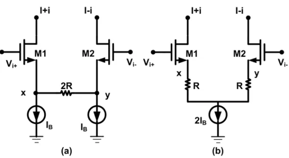
2.2.3 Source Degeneration
In the beginning, we introduce the source degeneration structure, which is the common structure in the transconductance circuit. The circuit is shown in Fig. 2.3.
Fig. 2.3 Transconductance using Source Degeneration Pair
In this circuit, the ideal operation of source degeneration is that Vi+ and V
i-perfectly follow to the ends of the resister. Then, the voltage across the ends of the resister, Vi+ and Vi-, will generate the output current. Because the output current is
generated by resister R, the linearity would be very great. However, the resisters between the gate and the source of the transistors M1, M2 are not zero, and they vary with the transconductance of M1, M2. Therefore, the input voltages would not perfectly follow to the ends of the resister R, and it would degrade the linearity. For this reason, lots of techniques are presented to solve this problem and increase THD.
As shown in [4], the output current to the input voltage can be got as:
2 ( ) 2 1 ( ) ( ) 2(1 ) 1 n n ox B n id id DS sat W C I L v i v N V N μ = − × + + (2.8) 1 1 m N G R N = + (2.9) From equation (2.9), the transconductance is proportional to the factor 1/R, so increasing the linearity by the resistor is also decreasing the transconductance. Using the Taylor series, the third harmonic distortion (HD3) can be derived as:
2 2 ( ) 1 1 3 ( ) ( ) 1 32 id DS sat v HD N V = × × + (2.10)
where the degeneration factor N is gm1,2×2R. From equation (2.10), the conclusion
could be made as: increasing the degeneration factor N, which increases the value R or the transconductances of M1, M2 (gm1, 2), can improve the HD3; therefore, the
linearity will be increased, as well.
Although the circuits in Fig. 2.3(a) and Fig. 2.3(b) shows the same voltage-to-current relationship, they present different properties. For Fig. 2.3(a), the tail currents will contribute differential noise in the output, which will dominate the noise performance. For Fig. 2.3(b), there are voltage drops in the resistors, which will reduce the range of the common mode voltage.
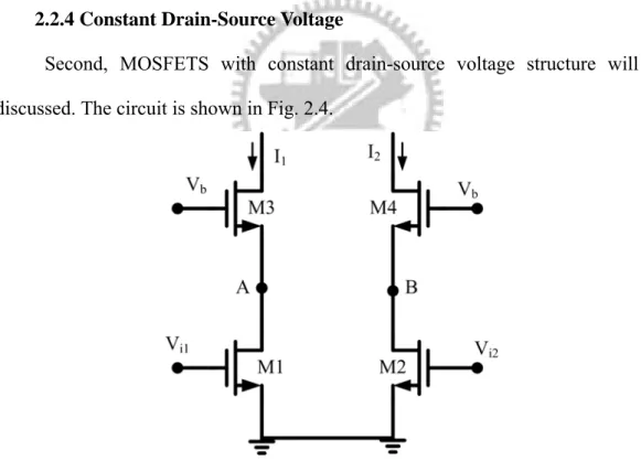
2.2.4 Constant Drain-Source Voltage
Second, MOSFETS with constant drain-source voltage structure will be discussed. The circuit is shown in Fig. 2.4.
Fig. 2.4 MOSFETS with Constant Drain-Source Voltage
In the circuit, the transistors M1 and M2 are in linear region, and M3 and M4 are in saturation region. Therefore, the output current I1 and I2 are as:
2 1 1,2 1,2 1 1,2 1,2 1 [ ( ) ] 2 ds i thn ds I =β V V −V − V (2.11)
2 2 1,2 1,2 2 1,2 1,2 1 [ ( ) ] 2 ds i thn ds I =β V V −V − V (2.12) Then the differential output current is:
1 2 1,2( 1 2)
o ds i i
I = − =I I βV V −V (2.13) From equation (2.13), the transconductance is proportion to βVds1,2. In practice,
second-order effects like mobility reduction and velocity saturation reduce the linearity somewhat. However, the linearity performance is dominated by the
variation of Vds1, 2. Therefore, some techniques are presented to fix the points A and
B to make the voltage Vds1, 2 constant.
2.3 Linearity-improved OTAs
As above, the four basic OTA circuits are introduced, and the major disadvantages of these circuits are the poor linearity. So lots of linearity enhancement techniques are presented to improve these problems. In this subsection, we will discuss two linearity enhancement techniques, which are already presented to improve the linearity.
2.3.1 Modified Source Degeneration OTA Circuits
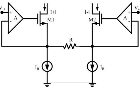
As discussion in subsection 2.2.1, the linearity will degrade since the input voltages do not perfectly follow to the ends of the resistor. Hence, the direct idea is that using op amps to make the input voltages follow to the ends of the resistor. This idea is shown in Fig. 2.5. The source voltages of M1 and M2 will be equal to the input voltages due to the virtual ground in each op amp. Hence the op amps would make the input voltages follow to the ends of the resistor more greatly than the original source degeneration.
Fig. 2.5 Improving the linearity of a fixed transconductor through the use of op amps
Another method for improving the linearity of a fixed transconductor is to force constant currents through M1 and M2 such that their Vgs are fixed which is shown in
Fig. 2.6. This modified source degeneration is added the negative voltage feedback, which will make the gate-source voltages of M1 and M2 constant. Therefore, it reduces the variation of the voltage across the resistor due to the constant gate-source voltages of M1 and M2.
Fig. 2.6 Improving the linearity of a fixed transconductor by maintaining a constant Vgs for M1 and M2
The circuits above which use negative voltage feedback to improve the linearity are not suitable for using as high speed OTA. Since the negative current feedback has larger bandwidth than the negative voltage feedback, the circuit using the negative current feedback will be introduced in next chapter.
2.3.2 Modified OTA Circuits with Constant Drain-Source Voltage
In subsection 2.2.2, MOSFETS with constant drain-source voltage are discussed, and the factor for the poor linearity is also discussed. The main factor is the variation of the drain-source voltages of M1 and M2 due to the input pair voltages and the temperature variation. Therefore, it needs a circuit to fix the voltages constant, and the op amps are used for this purpose. The circuit is shown in Fig. 2.7. Due to the virtual ground of the input pairs, the drain-source voltages of M1 and M2 will be fixed to the voltages of the positive input voltages in op amps. Hence, the positive input voltages in op amps could also use to tune the transconductance, which could be seen as below:
1 2 ( 1 2)
o tune i i
I = − =I I βV V −V (2.14) Thus, using op amps could fix the voltage which is the main factor for the linearity reduction. The op amps should be designed for simpler circuits to reduce the complexity and noise which the fewer devices using the less noise will be contributed.
Chapter 3
Proposed OTAs for High Speed
Applications
3.1 Introduction
As discussion in chapter 2, the main disadvantage of the OTAs is the poor linearity. Therefore, lots of linearity enhancement techniques are presented to improve the shortcoming. In the latter of chapter 2, two techniques of them are introduced. However, these two methods are not suitable to high speed applications, since the negative voltage feedback has lower bandwidth, which will reduce the loop gain at the frequency we wish to operate. Hence, the two modified circuits are proposed to apply in the high speed applications in this chapter.
3.2 Proposed Source Degeneration OTA with Negative Current
Feedback
In this section, the linearity enhancement techniques are proposed by using negative current feedback, which is more suitable in high speed applications. Since the resistance in the current feedback is smaller than that in the voltage feedback. Therefore, the current feedback circuit features a very high bandwidth for higher
pole location [7]. This means that the linearity voltage feedback circuit improved will be less because the loop gain in the high frequency will be not sufficient due to the lower bandwidth. For this reason, the modified circuit using negative current feedback is proposed to put in use in the high speed applications.
3.2.1 Characteristics and Operation of the OTA Circuit
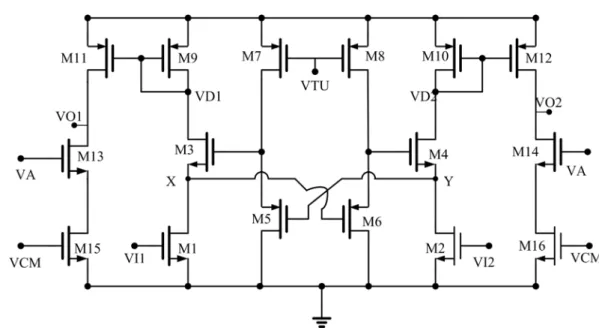
The modified circuit using negative current feedback is shown in Fig. 3.1.
Fig. 3.1 Modified Source Degeneration Circuit using negative current feedback The transistors M9~M16 are the output stage. The modified structure uses M17 operating in the linear region to replace the resister 2R in the conventional source degeneration circuit. That is because this circuit could utilize the gate voltage (VD) as tuning circuit. Therefore, it can be used to overcome the variation due to the fabrication or temperature variations. The operation of transistors M1~M4 and M17 is the same as the description in subsection 2.2.1. However, the transistors M5~M8 are added to increase the THD. These transistors are composed of the negative current feedback circuit, and it provides a negative feedback gain to degenerate the
HD3. Consequently, it could achieve the requirement of HD3 without large value of R.
At first, the operation of the negative current feedback circuit is presented. Assume input voltage Vi1 increases, but the voltage at the point x (Vx) does not
follow this variation. This will make the voltage between the gate and the source of M1 increase. Therefore, the drain current of M1 increases, and the drain current of M9 increases, too. Because the drain current of M9 increases, the voltage across the drain and the source of M9 also increases. For this reason, the gate voltage of M5 (Vg5=VDD-Vds9) decreases. Then, the Vgs of M5 decreases, and the drain current of
M5 also decreases. The decreasing current will flow to the main circuit through the current mirror pair M3 and M7. Therefore, the drain current of M1 will be pulled down, and the voltage Vx will be pushed up. Therefore, the negative current
feedback circuit could give the voltage Vx a hand to follow the variation of the input
voltage. Similar, the voltage Vy will also follow with the input voltage Vi2 by the
same operation.
By the way, the math formulas for HD3 will be derived to prove the concept of the circuit. First, assuming Vi1= vid + vcm, Vi2= vid – vcm, and the voltages at the point
x, y are Vx, Vy. Therefore, the drain currents of M1 and M2 are as below:
1 1,2( 1 ) D m i x I =g V −V (3.1) 2 1,2( 2 ) D m i y I =g V −V (3.2) As well, the current across the transistor M17 (rds17) can be got as:
17 x y xy ds V V I r − = (3.3) Hence, the drain currents of M1 and M2 can also be described as:
1 3
D D xy
2 4
D D xy
I =I −I (3.5) where ID1+ID2=ID3+ID4=2IB, which IB is the bias current. From equation (3.1), (3.2),
(3.4), and (3.5), the differential output current is as below:
1 2 1,2( ( )) 2 3 4
o D D m id x y xy D D
I =I −I =g v − V −V = I +I −I (3.6) Now, we assume Ro is the resistance looking down the drain of M1, and also assume
Ro is constant for simplicity. Thus, the drain currents of M3 and M4 could be
determined by the drain currents of M5 and M6 due to the current mirror pairs. So the currents are shown below:
2 3 5,6( 1 5,6 5,6) D D o gs thn I =β I R −V −V (3.7) 2 4 5,6( 2 5,6 5,6) D D o gs thn I =β I R −V −V (3.8)
Using equation (3.7), (3.3), (3.8), and (3.6), the relation between the differential output current and the voltage across M17 is shown in the following:
1 2 1 2 17 2 x y ( ) D D D D ds V V I I I I r α − − = + − (3.9) where we assume the negative current feedback gain is α=β5,6Ro ×(2Vgs5,6 +
2Vthn5,6-2IBRo). The value β5,6 is proportion to 1/RV, so the unit of negative current
feedback gain α is V/V. Furthermore, from equation (3.9) and (3.6), the equation about the voltage across M17 can be described as:
(1 ) (1 ) 1 id x y Nv V V N α α + − = + + (3.10) where N=gm1,2×rds17 is the source degeneration factor [4]. Finally, for the drain
formulas of M1, M2, and the equation (3.10), we can get the relation about differential output current and the input voltage.
2 1 1,2( 1 1,2) D i x thn I =β V − −V V (3.11) 2 2 1,2( 2 1,2) I =β V −V −V (3.12)
2 1 2 ( ) 4 1 ( ) ( ) 2(1 (1 ) ) 1 (1 ) n B id o D D id DS SAT I v I I I v N V N β α α = − = − × + + + + (3.13) 17 1 1 (1 ) m ds N G r α N = + + (3.14) From equation (3.14), the transconductance is approximately proportional to the factor 1/ (1+α), which we can achieve the requirement of linearity with reduction of transconductance with about factor (1+α) rather than the factor rds17 for the
traditional source degeneration circuit. Hence, improving the linearity by negative feedback gain would reduce the smaller value of transcoductance than the traditional circuit. Using the Taylor series, the third harmonic distortion (HD3) could be got as:
2 2 ( ) 1 1 3 ( ) ( ) 1 (1 ) 32 id DS SAT v HD N V α = × × + + (3.15)
As compared with equation (2.2), the factor N in equation (2.2) change to (1+α)N in equation (3.15). Therefore, it can also improve the HD3 by the negative current feedback gain, α. Thus, the linearity could be achieved without large value rds17,
and this relaxes the degeneration factor N and reduces the area due to the smaller resistance rds17.
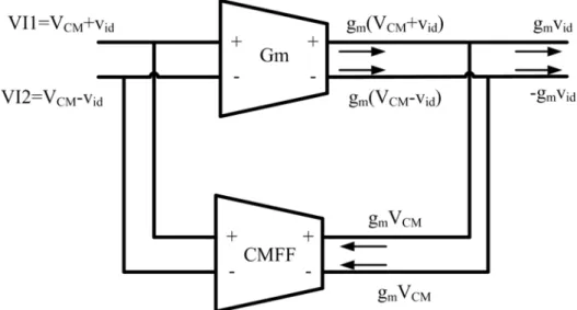
3.2.2 Common Mode Feedback Circuit
In the filter designs, the output of the OTA must connect to the input of the next OTA, so the common mode voltage is very important. Now, two circuits will be shown to understand the need of the common mode feedback circuit [8]. First, a simple differential amplifier which the inputs and outputs are shorted is shown in Fig. 3.2. We can find the common mode voltages of inputs and outputs are well defined as VDD-ISSRD/2.
Fig. 3.2 a simple differential amplifier with inputs shorted to outputs
However, another circuit is shown in Fig. 3.3. Due to the fabrication process, the mismatches in the current mirrors will cause finite difference between ID3, 4 and
ISS/2. If ID3, 4 is slightly greater than ISS/2, M3 and M4 will enter the linear region to
make their drain currents equal to ISS/2. Conversely, if ISS/2 is slightly greater than
ID3, 4, M5 will enter the linear region to make ISS/2 equal to ID3, 4. Hence, due to the
non-well defined common mode output voltages, it would make the transistors enter the wrong regions and would reduce the bias current, as well. Therefore, it needs a common mode feedback circuit for the differential circuits to fix the common mode output voltages at the wished level.
Fig. 3.3 High-gain differential pair with inputs shorted to outputs
Therefore, the common mode feedback circuit is needed to stabilize the output common mode level, which is shown in Fig. 3.4. Note that the output common mode level is fixed to the input common mode level. It is because the outputs of the OTA connect to the inputs of the next OTA by designing a filter. The following will describe the operation of the common mode feedback circuit [9].
Fig. 3.4 The common mode feedback circuit for modified source degeneration using negative current feedback
MF10 and MF11 connect to the output stage M13, M14, M15, and M16 in Fig. 3.1 and it will adjust the output common mode level due to the feedback current. For example, if the output common mode voltages are larger than the reference voltage Vref, the drain current of MF8 will increase. Hence, the currents in the output stage
in Fig. 3.1 will increase, as well. Because the voltage across M11 and M12 increase due to the increased currents, the output common mode voltages decrease. Conversely, if the output common mode voltages are smaller than the reference voltage Vref, the smaller current will flow to the output stage to increase the output
common mode voltage. In addition, the operation of the common mode feedback circuit can be interpreted by the voltage concept. There is a negative gain from the gates of MF1, MF2 to the drains of them, and the gain from the gate of MF9 to the outputs in Fig. 3.1 is a positive gain. Therefore, the common mode feedback circuit provides a negative gain for the outputs, so it can fix the output common mode voltages to the reference voltage Vref. When the circuit operates at high frequency,
the common mode feedback circuit must also be stable at high frequency. The open loop gain of the common mode feedback circuit is:
(
)
CMFB CMFB 1, 2 8 11 ( ) ( ) 1 1 1 out mf mf out A B L out mf mf A s g s R g R C C s s sC R g g ≅ × × = ⎛ ⎞⎛ ⎞ + + + × ⎜ ⎟⎜ ⎟ ⎜ ⎟⎜ ⎟ ⎝ ⎠⎝ ⎠ (3.16)where CA and CB are the total capacitance in the points A and B. From equation
(3.16), the pole at 1/ (CL×Rout) is the dominated pole, and the poles at gmf8/CA,
gmf11/CB are the non-dominated poles. They must be pushed far away the unity gain
frequency to increase the phase margin.
3.2.3 Noise Analysis
For the communication systems, the noise is the major course to avoid that the signal could be received correctly. However, there are noises in the devices such as flicker noise and the thermal noise. If the frequency is less than the corner frequency, the dominated noise is the flicker noise; otherwise, the dominated noise is the thermal noise. Since the cutoff frequency for the implement filter is at high frequency, the dominated noise is the thermal noise. The channel noise can be modeled by a current source connected between the drain and the source with a special density as:
2 4 ( )2 3
n m
I = kT g (3.17) where k is the Botzmann constant, T is the absolute temperature, gm is the source
conductance. Using the thermal noise model, the total output-referred noise spectral density of the modified source degeneration circuit using negative current feedback is derived as: 2 1 2 , 9 1 1 17 2 1 17 17 3 1 17 2 1 17 5 1 17 2 2 1 4[4 ( ) ] 2[4 ( ) ]( ) 3 3 1 (1 ) 2 2 {2 4 ( ) 4[4 ( ) ]}( ) 3 3 1 (1 ) 2 2[4 ( ) ]( ) 3 1 (1 ) m out n m m m ds m ds m m m ds m ds m m ds g I kT g kT g g r g r kT g kT g g r g r kT g g r α α α = + + + + + + + + + + [ ] (3.18)
where α is the negative current feedback gain. The input-referred noise spectral noise density could be calculated as:
2 , 2 , 2 1 1 17 ( ) 1 (1 ) out n in n m m ds I V g g r α = + + (3.19)
From equation (3.18), the added current feedback circuit provides additional noise in the output, but increasing the current feedback gain could reduce the noise. As well, the large aspect ratios of the input transistors and small aspect ratios of the load transistors should be designed for small output noise. However, the input-referred
noise is larger than the traditional circuit due to the added current feedback circuit.
3.3 Proposed OTA Circuit with Constant Drain-Source Voltage
As mentioned in the chapter 2, MOSFET with constant drain-source voltage would degrade the linearity due to the variation of the drain-source voltage in the input pairs, and the enhancement technique using op amps to fix the drain-source voltages is presented. Therefore, the op amps should be designed as simple as possible to reduce the complexity.
3.3.1 Characteristics and Operation of the OTA Circuit
In [10], an approach uses feedforward method instead of the op amps to fix the drain-source voltage of the input pairs. However, the circuit used in [10] stacks five transistors and could not work at lower power supply, which operated at +-1.4V. As the transistors sizes are smaller, the power supply voltage will be lower. Therefore, the circuit in [10] will be not suitable for lower power supply. For this reason, the modified circuit will be proposed in this section. The whole circuit is shown in Fig. 3.5.
The transistors M9~M16 are the output stage. The transistors M1~M4 are the same transistors as shown in Fig. 2.7, and the regions and characteristics are the same as before. However, the transistors M5~M8 are used to replace the op amps. The circuits can not only tune the linearity but also the unity gain frequency. Furthermore, the OTA could operate at the lower power supply than the circuit in [10].
At first, the operation of the feedforward circuit is presented. Assume there are large differential signals in the input pairs, which is the voltage in VI1 is increased, and the voltage in VI2 is deceased. If the voltages between the gate and source of M3 and M4 do not follow the variations in the input pairs, the drain voltage of M1 will decrease, and the drain voltage of M2 will increase to make Id1=Id3 and Id2=Id4.
However, the variations in the drains of the input pairs will degrade the linearity, and the feedforward-regulated circuit is used to overcome the problem of the variations. When the source voltage of MOS M3 decreases, the gate voltage of MOS M4 decreases, which is due to the source follower circuit, M6 and M8. Since the gate voltage of M4 decreases, it would make the drain voltage of M2 decreases, too. Therefore, the drain voltage of M2 could be fixed to a constant value by the feedforward-regulated circuit. The drain voltage of M1 will also be fixed to a constant value by the similar operation.
By the way, the math formulas for the output current to the input voltage will be derived to prove the concept of the circuit. First, we make the following assumption VI1 = VCM +vid, VI2 = VCM -vid, Vx = VDS + ΔVD, and Vy = VDS – Δ
VD. In Fig. 2.2, if the drain-source voltages of input pairs are constant, the relation
between output current and input voltage is:
1 2 2 1,2 ( 1 2) 2 1,2 (2 )
D D DS DS id
The transconductance is proportion to β1,2VDS, and could be very linear. However,
since the drain-source voltages of input pairs vary with the temperature, fabrication processing and the input signal, the relation between output current and input voltage will become as:
1 2 2 1,2[ ( 1 2) ( 2 1,2) 2 ] D D DS D CM thn D DS I −I = β V VI −VI + ΔV V − V − ΔV V 1,2 1,2 2β [VDS(2 )vid V VD( CM 2Vthn ) 2 V VD DS] = + Δ − − Δ (3.21) Due to the variation of the drain-source voltage ΔVD, the linearity degrades.
Therefore, the proposed circuit will reduce the variation, which could find out as follow. By the regions in the transistors M1~M4, the current formulas can be got as:
2 1 1,2 1,2 1 2 [ ( 1 ) ] 2 D x thn x I = β V VI −V − V 2 3,4(Vy Vgs7,8 Vx Vthn3,4) β = + − − (3.22) 2 2 1,2 1,2 1 2 [ ( 2 ) ] 2 D y thn y I = β V VI −V − V 2 3,4(Vx Vgs7,8 Vy Vthn3,4) β = + − − (3.23) From the source follower circuits, based on ID5 = ID7 and ID6 = ID8, the voltage Vgs7, 8
could be got as:
5,6 7,8 5,6 7,8 7,8 ( | |) | | gs DD thp thp V β V VTU V V β = − − + (3.24) From equation (3.20) as well as (3.21), the differential output current and the
variation of the drain-source voltage of the input pairs are as below:
1 2 3,4 3,4 7,8 1,2 1,2 1,2 3,4 7,8 3,4 2 ( ) 2 1 ( ) ( ) 2 D D x y D thn gs DS id thn DS CM gs thn I I V V V V V V v V V V V V β β β β − − = Δ = − = + − − − (3.25)
1 2 1,2 1,2 3,4 7,8 3,4 2 1 2 ( ) DS id o D D DS CM thn gs thn V v I I I V V V V V β β = − = − − + − (3.26)
Based on equation (3.25) and (3.26), the variations on the drain-source voltages on input pair could be tuning by varying the drain-source voltage Vx, Vy of the input
pair, which can be also varied by the voltage VTU. As well, reducing the variation in the drains of the input pairs will decrease the transconductance, which means it is tradeoff for the linearity and transconductance. However, increasing Vgs7, 8 will also
increase noise as described after.
3.3.2 Common Mode Feedback and Feedforward Circuits
For fully differential circuit, the common mode gain can be reduced by increasing the output resistance of the tail current [11]. However, there is a voltage drop in the tail current, and that would reduce the headroom of the input voltage. So pseudo-differential circuits are used to increase the headroom, which take off the tail current from the fully differential circuit. However, the pseudo-differential circuits have a shortcoming comparing with the fully differential circuits for their common mode rejection ratio (CMRR). Since the half circuits of the pseudo-differential circuits for common mode and differential mode are the same, the common mode gain and the differential gain are almost the same, i.e., CMRR=ADM/ACM=1. This
large ACM, in the pseudo-differential circuits, would lead to huge common mode
variations at the OTA outputs. Hence, a common mode feedforward circuit is needed for pseudo-differential circuit to reduce the common mode gain. The concept of the common mode feedforward circuit can be shown in Fig. 3.6. It is obviously that the common mode feedforward circuit will generate the common mode current. This current will flow to the output stage and cancel the common mode of the output current. Therefore, the common mode of the output current is reduced, but the
differential mode does not influence, which the CMRR increases.
Fig. 3.6 The concept of the common mode feedforward circuit
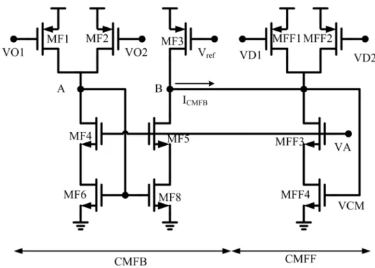
As well, the common mode feedback circuit is needed to fix the output common mode voltage to the reference voltage Vref. The common mode feedback
and feedforward circuit is shown in Fig. 3.7 [12]. Now, we first discuss the common mode feedback circuit. The transistors MF1 and MF2 will detect the output common mode current, and this current will compare the reference current due to the current mirror pair. If the output common current is larger than the reference current which means that the common mode voltage is greater than the reference voltage, the feedback current ICMFB will increase to make the output common mode voltage
decreasing. Conversely, the feedback current will decrease to fix the common mode voltage to the reference voltage Vref.
Fig. 3.7 The common mode feedback and feedforward circuit for modified circuit of MOSFET with constant drain-source voltage
Next, we will see the operation of common mode feedforward circuit. The transistors MFF1, MFF2 in Fig. 3.7 and M9, M10 in Fig. 3.5 are current mirrors, so the input common mode current will be detected by the circuit. This current will flow to the output stage to cancel the common mode current as discussion before.
Finally, the common mode control circuit must be also stable at high frequency, which needs enough phase margin at high frequency. The open loop gain for the common mode feedback circuit is:
(
)
CMFB CMFB 1, 2 6 4 ( ) ( ) 2 1 1 1 out mf mf out A B L out mf mff A s g s R g R C C s s sC R g g ≅ × × = ⎛ ⎞⎛ ⎞ + + + × ⎜ ⎟⎜ ⎟ ⎜ ⎟⎜ ⎟ ⎝ ⎠⎝ ⎠ (3.27)where CA and CB are the total capacitance in the points A and B. From equation
(3.27), the pole at 1/ (CL×Rout) is the dominated pole, and the poles at gmf6/CA,
gmff4/2CB are the non-dominated poles. They must be pushed far away the unity gain
3.3.3 Noise Analysis
Thermal noise:
As discussion in subsection 3.2.3, the dominated noise is the thermal noise in high frequency. Hence, the output-referred noise spectral density of the constant drain-source voltage using feedforward circuit is as:
2 1,2 2 , 1 1,2 1,2 3,4 7,8 3,4 7 5 2 2 3,4 7,8 3,4 2 2 7 5 7 5 3 2 2 1 2[4 ( )] 3 ( ) 2 1 ( ) 2 2 2[4 ( )] 2[4 ( )] 2 1 3 3 2[4 ( )] ( ) ( ) ( ) 3 4[4 ( DS out n DS m CM thn gs thn m m gs thn ds ds ds ds m V I kT V g V V V V kT g kT g kT V V g g g g g kT β β β β ⎛ ⎞ ⎜ ⎟ ⎜ ⎟ ⎜ ⎟ = ⎜ ⎟ − − ⎜ ⎟ + ⎜ ⎟ ⎜ − ⎟ ⎝ ⎠ ⎡ ⎤ ⎢ ⎥ +⎢ + + ⎥× − + + ⎢ ⎥ ⎣ ⎦ + 2)] 9 3 gm (3.28)
where the parameters in (3.28) are the same as subsection 3.2.1. Also, the input-referred noise spectral density could be calculated as:
2 , 2 , 2 1,2 1,2 1,2 3,4 7,8 3,4 2 ( ) 2 1 ( ) out n in n DS DS CM thn gs thn I V V V V V V V β β β = ⎛ ⎞ ⎜ ⎟ ⎜ ⎟ ⎜ ⎟ ⎜ ⎟ − − ⎜ ⎟ + ⎜ ⎟ ⎜ − ⎟ ⎝ ⎠ (3.29)
For the constant drain-source voltage without feedforward circuit, the thermal noise due to the MOS M3 and M4 is as:
2 3 3 3 1 2 1 2[4 ( )] ( ) 3 1 m m m ds g kT g × +g r (3.30) However, from the second term in (3.28), the noise due to M3 and M4 is In2*β3,42
(Vgs7,8-Vthn3,4)2=In2*gm32 for Vg3=Vg4. This is because the drain voltages of M1 and
small signal, so the resistance rds1 does not influence the noise due to M3 and M4.
As well, the large aspect ratios of the input transistors and small aspect ratios of the load transistors should be designed for small output noise. When the voltage Vgs7,8
increases to reduce the variation ΔVDS in (3.25) and increase the transconductance
in (3.26), the output-referred noise also increases as shown in (3.28). However, the input-referred noise is larger than the traditional circuit due to the added current feedforward circuit.
Chapter 4
Transconductance-C Filters
4.1 Introduction
In recent years, there are lots of filter synthesis techniques presented. In these techniques, not all of them are suitable for the design of high speed filters. As described in chapter 1, the sampled-data analog filters, RC active filters and MOSFET-C filters are not suitable for high speed filter designs. However, the transconductance-C filters could be operated at high frequency. Hence, the transconductance-C filters will be introduced in this chapter [13].
For the transconductance-C filter designs, the basic building elements are transconductors and capacitors. In filters structure, the capacitor could be grounded or floating. In section 4.2, the ransconductance-C integrators will be described, and it will also discuss the non-ideal effects for the first order filters. In section 4.3, the 4th order biquad filter will be introduced, which is the filters we used. The blocks which using transconductors as resistors will discuss in this section, and next the biquad section and 4th order filter cascading two biquad section will also be discussion. Finally, the output buffers will be described, which avoid the influence of the output devices.
4.2 Transconductance-C Integrators
In this section, the fundamental transconductance-C filter is discussed. First, the ideal integrator model for transconductance-C filter is described. For ideal transconductors, they have infinite output resistance, infinite bandwidth etc. However, the transconductors are not ideal in the real world. Hence, the non-ideal effects of the transconductors will be described in subsection 4.2.2.
4.2.1 Integrator Model
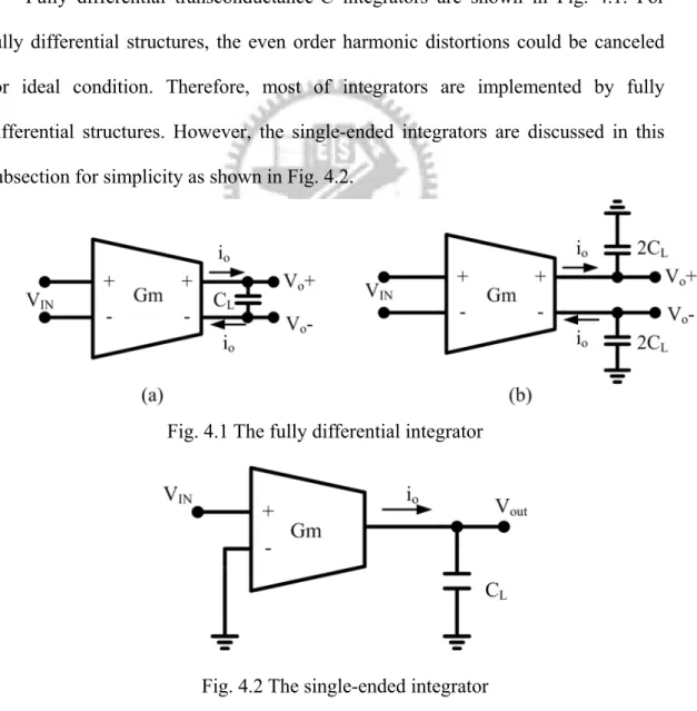
Fully differential transconductance-C integrators are shown in Fig. 4.1. For fully differential structures, the even order harmonic distortions could be canceled for ideal condition. Therefore, most of integrators are implemented by fully differential structures. However, the single-ended integrators are discussed in this subsection for simplicity as shown in Fig. 4.2.
Fig. 4.1 The fully differential integrator
Fig. 4.2 The single-ended integrator
infinite output resistance, and the output voltage in this integrator could be derived as: ( ) ( ) ( ) out m IN L V s g H s V s sC = = (4.1) with s=jω, which equation (4.1) could be described as H(jω) = gm/jω×CL = [R(jω)
+jX(jω)]-1. In equation (4.1), we can see that the ideal integrator has infinitely high DC gain. As well, since phase margin defines as PM=-180°+tan-1(X(jω)/R(jω)) and quality factor defines as Q(jω)=X(jω)/R(jω), the ideal transconductor has PM=-90° for all frequencies and infinite quality factor. Finally, the unity gain frequency for the integrator is:
m T L g C ω = (4.2)
4.2.2 Non-ideal effects in the integrator
For non-ideal tranconductors, they have non-zero output conductance and a delay in transfer function. Since transconductors have parasitic poles and zeros, there is a delay in the integrator transfer function. However, these poles and zeros effects could be modeled with a single effective zero due to parasitic poles and zeros locating at much higher frequency than the unity gain frequency. The zero could be at right complex half-plane (RHP) for the phase lag or at left complex half-plane (LHP) for the phase lead.
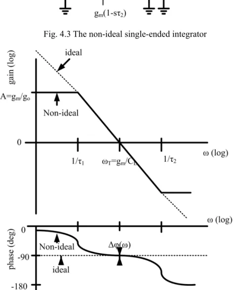
The non-ideal integrator could be modeled as Fig. 4.3. From Fig. 4.3, the transfer function for this non-ideal integrator is:
2 2 1 ( ) 1 1 ( ) 1 1 out m nonideal L IN o o V s g s s H A C V s g s s g τ τ τ − − = = = + + (4.3)
Hence, there are finite dominate pole and DC gain due to the non-zero output conductance given as:
1 L, m o o g C A g g τ = = (4.4) In Fig. 4.4, the ideal as well as non-ideal magnitude and phase responses are given. Normally |1/τ1|<<ωT<<|1/τ2|.
Fig. 4.3 The non-ideal single-ended integrator
Fig. 4.4 Gain and phase of an ideal integrator and a non-ideal integrator From Fig. 4.4, the finite DC gain and the parasitic zero cause the deviation of the integrator phase from -90°. The phase error is defined as:
( ) arg[Hnonideal( )] 90
ϕ ω ω
This error is a principal source of errors in filters. Next, we rewrite the transfer function as: 1 ( ) ( ) ( ) nonideal H R jX ω ω ω = + (4.6) Hence, the quality factor of an integrator is defined as:
( ) ( ) tan( arg( ( ))) ( ) nonideal nonideal X Q H j R ω ω ω ω = = − (4.7) From equation (4.3), (4.6), and (4.7), we can get the reciprocal value of the quality factor as: 2 1 1 1 ( ) nonideal Q ω ≈ωτ −ωτ (4.8) From equation (4.8), the quality factor is infinite at the frequency which is the geometric mean of the dominant pole and the effective parasitic zero. Note that this condition holds as the output conductance go and the delay τ2 have the same sign.
The phase at that frequency is also exactly -90°.
4.3 Fourth order filter by cascading two biquad sections
In this section, the 4th order filter is presented. Since the proposed OTAs are used to compose of 4th order filter, the filter must be introduced. However, we will first introduce the resistor and inductor blocks, and then a biquad section will be discussed. Finally, the 4th order filter and output buffers will be described.
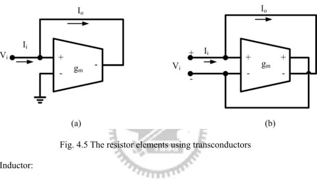
4.3.1 Resistor and inductor blocks
Since RLC are the basic elements for composing of the filters, the following will introduce the methods using the transconductors as resistors and inductors [14]
Resistors:
First, the resistor model is discussed. The Fig. 4.5 shows the resistor configuration for single-ended transconductor and differential transconductor. In Fig.
equal to the transconductance output current Io as:
i o m i
I =I =g V (4.9) Thus, the configuration represents a resistor as its equivalent resistance as:
1 i i m V R I g = = (4.10) Note that it must maintain negative feedback when forming the gm-based resistor. If the feedback connection becomes positive, the resistance will be negative.
Fig. 4.5 The resistor elements using transconductors Inductor:
In the following, the inductor element for using transconductor is discussed. The configuration for this element is shown in Fig. 4.6. From Fig. 4.6, the current equations could be:
1 m2 2
I =g V (4.11) 2 m1 1
I =g V (4.12) Also, based on the voltage across the capacitor C, the following equation could be got. 2 2 1 V I sC = × (4.13) Hence, the inductor using transconductor block can be got as its inductance being:
1 2 1 1 2 2 1 2 1 1 m m m m V I sL sC I g g V g g = = = (4.14)
Fig. 4.6 The inductor elements using transconductors
4.3.2 Biquad Section
The passive RLC circuit of the GIC biquad is shown in Fig. 4.7. From this figure, the transfer function is as:
2 1 1 1 1 1 V R V sC R sL = + + (4.15)
Fig. 4.7 The second order bandpass filter for passive RLC prototype Using the elements discussed in subsection 4.3.1, the active biquad section could be shown in Fig. 4.8 for the single-ended and differential models.
Fig. 4.8 The second order bandpass and lowpass filter for active transconductance-C prototype
For R = 1/gm1 and L = C2/gm3gm4, the transfer function for bandpass filter will
be: 2 1 2 2 1 1 2 2 2 3 4 m m m m sC g V V = −s C C +sC g +g g (4.16) Using the fact that
3 2 2 m Lo g V V sC = − (4.17) The transfer function for lowpass filter is:
1 3 2 1 1 2 2 2 3 4 Lo m m m m m V g g V = s C C +sC g +g g (4.18) The advantage of the biquad section is the cascade fashion, and the loop is very stable at higher order filter. The disadvantage is the loading effect, and the
sensitivity of the biquad section to component variation is larger than the LC-ladder structure.
4.3.3 4th Order linear-phase Filter
The implement 4th order filter by cascading two biquad sections is shown in Fig. 4.9. Since the outputs in second and fourth transconductors of a biquad section are
connected together with the output in first transconductor, it needs a common mode feedfack circuit to fix the outputs of the three transconductors to the reference voltage. The common mode feedforward circuit in each transconductor depends on the requirement of the transconductor.
Fig. 4.9 The 4th order lowpass filter
From equation (4.18), the cutoff frequency ω0 and the quality factor Q for a
biquad section can be expressed as:
1 0 m g C ω = (4.19) 1 2 m p m g Q g = (4.20) 1 K = (4.21) From equation (4.19), the unity gain frequency of the first transconductor in the