I
國 立 交 通 大 學
光電工程研究所碩士班
碩 士 論 文
熱退火條件之於 IGZO 金屬氧化物薄膜電晶
體特性影響之研究
Influence of Ambient Atmosphere on
Thermal-Annealing Amorphous IGZO TFTs
研 究 生 : 袁煥之 Huan-Chih Yuan
指導教授 : 冉曉雯 教授 Prof. Hsiao-Wen Zan
蔡娟娟 教授 Prof. C.C. Tsai
熱退火條件之於 IGZO 金屬氧化物薄膜電
晶體特性影響之研究
Influence of Ambient Atmosphere on
Thermal-Annealing Amorphous IGZO TFTs
研 究 生 : 袁煥之 Student : Huan-Chih Yuan
指導教授 : 冉曉雯 教授 Prof. Hsiao-Wen Zan
蔡娟娟 教授 Prof. C.C. Tsai
國 立 交 通 大 學
光電工程研究所碩士班
碩 士 論 文
A Thesis
Submitted to Department of Photonics
College of Electrical Engineering and Computer Science
National Chiao Tung University
in Partial Fulfillment of the Requirements
for the Degree of
Master
in
Display
July 2009
Hsinchu, Taiwan, Republic of China
I
熱退火條件之於 IGZO 金屬氧化物薄膜電晶體
特性影響之研究
研究生:袁煥之 指導教授:冉曉雯 教授
蔡娟娟 教授
Chinese Abstract
國立交通大學
光電工程研究所
摘 要
在本文中,我們對低溫下沉積的 a-IGZO 薄膜電晶體的不穩定性進行了研 究。在連續量測七次 IDVG的電性後,發現此不穩定元件的 Von 會有很嚴重的偏移 現象。這暗示了在低溫濺射的沉積過程中,主動層薄膜裡面原子之間的鍵結是不 夠的完整的。因此,在通道與絕緣層的介面上產生了缺陷態。 另外,本文也討論了環境對於熱退火的影響。藉由改變熱退火時的氛圍,觀 察 a-IGZO 薄膜電晶體的電性分析。在量測時,觀察到 a-IGZO 薄膜電晶體在真 空環境熱退火與在大氣環境熱退火會有截然不同的現象。在真空環境底下熱退火 後的元件會隨著退火溫度的升高呈現導通的現象。想反地,在大氣環境底下熱退 火後的元件會隨著退火溫度的升高呈現絕緣的現象。本實驗藉由熱脫附質譜術(TDS)與 X 光光電子能譜(XPS)來探討此現象的機制。經過分析與討論後,確認氧 原子會因為不同環境下熱退火的處理會有進入與跑出薄膜裡面的兩種行為。另 外,此篇論文之研究,是與周政偉學長與陳蔚宗學長所共同進行開發的。
III
Influence of Ambient Atmosphere on
Thermal-Annealing Amorphous IGZO TFTs
Student:Huan-Chih Yuan Advisor:Prof. Hsiao-Wen Zan
Prof. C.C. Tsai
Department of Photonics
National Chiao Tung University, Hsinchu, Taiwan
English Abstract
Abstract
The stability of as-deposited a-IGZO TFTs was studied. The serious turn-on
voltage shift under seven times sequent IDVG measurement of unstable as-deposited
device was observed. It suggests that the atomic bonding of film was loose due to low
temperature during sputter process. Hence, the defects were formed in the interface
between channel and dielectric layer.
By varying the post-annealing ambiance, it was observed that the transfer
characteristic of a-IGZO TFTs annealed in vacuum based furnace and atmosphere
toward to conductive with increasing temperature. In the contrary, the device annealed
in atmosphere based went toward to insulate with increasing. The mechanism was
investigated by the thermal desorption spectrometry (TDS) and X-ray photoelectron
spectroscopy (XPS). It was confirmed that the post-annealing could introduce oxygen
into IGZO film or extract oxygen from IGZO film depending on the annealing
ambiance. Besides, this work was studied with my senior classmates, Cheng-Wei
V
致謝
Acknowledgement
時光飛逝,在交大的這兩年的碩士研究生活,也將圓滿的畫下句點。記得兩 年前剛來找指導教授,老師親切的接待彷彿一切都在眼前。誠摯的感謝我的兩位 指導教授,冉曉雯博士與蔡娟娟博士。謝謝老師在學業上與實驗上的細心指導與 教誨,並指點我正確的方向,以及對研究態度的嚴謹,而老師對於事物的遠見及 胸襟更是我未來努力學習的方向。在此對老師致上內心最誠摯的誠意與謝意,使 我在這兩年中獲益匪淺。 回首這兩年,實驗室裡共同的生活點滴也是我最美好的回憶。感謝實驗室裡 的每一個人,有了大家的陪伴讓我在研究時充滿動力,生活充滿歡樂。感謝實驗 室周政偉學長、陳蔚宗學長、馬文元學長、顏國錫學長、高士欽學長、蔡武衛學 長、黃彥棠學長對我平時的照顧並給予我研究實驗的幫忙與建議。特別感謝周政 偉學長與陳蔚宗學長,感謝兩位學長的悉心指導與討論,在我有研究上的問題 時,願意仔細詳盡的為我解答,給了我很大的幫助。感謝黃慶能、曾威豪、陳達 欣、王建敏、姚芳弘、姜淑玲、姜鈞銘、孟繁琦、歐陽祥睿、吳玉玫、古明哲、 李建亞、薛琇文、許宏榮、許翼鵬、羅世益、鄭柏翔、許庭毓、李唯碩,謝謝你 們的支持與陪伴,我真的萬分的珍惜與感激。特別感謝黃慶能、薛琇文、羅世益, 謝謝你們在實驗上面的幫忙,讓我的實驗得以順利完成。 最後,我要感謝我的家人,尤其是我的母親,多年來辛苦的栽培與教誨,你們無悔的付出與支持,讓我順利完成我的學業。我真的很愛你們! 在此我要獻上 內心最深的謝意。
VII
Contents
CHINESE ABSTRACT I
ENGLISH ABSTRACT III
ACKNOWLEDGEMENT V
CONTENTS VII
FIGURE CAPTIONS IX
TABLE CAPTIONS XI
CHAPTER1 GENERAL INTRODUCTION 1
1.1 INTRODUCTION 1
1.2 THE MECHANISMS OF A-IGZOTHIN FILM TRANSISTORS 3
1.2-1 Small electron effective mass [17] 4
1.2-2 Unique chemical bonding 5
1.2-3 Percolation conduction model 5
1.2-4 Tunable carrier concentration 6
1.2-5 Composition of a-IGZO 7
1.3 MOTIVATION 7
FIGURES OF CHAPTER 1 8
CHAPTER2 EXPERIMENTAL PROCEDURE 12
2.1 DEVICE STRUCTURES AND FABRICATION 12
2.1-1 Dielectric deposition 12
2.1-2 a-IGZO film deposition 13
2.1-3 Source/Drain deposition 14
2.1-4 Post-annealing 14
2.2 ANALYSIS INSTRUMENTS 15
2.2-1 X-ray photoelectron spectroscopy (XPS) 15
2.2-2 Thermal desorption spectrometry (TDS) 16
2.2-3 X-ray diffraction (XRD) 16
2.3 METHODS OF DEVICE PARAMETERS EXTRACTION 18
2.3-1 Mobility 18
2.3-3 Sub-threshold swing (S.S.) 19
2.3-4 Turn-on voltage (Von) 20
2.3-5 Threshold voltage (Vth) 20
FIGURES OF CHAPTER 2 22
CHAPTER3 RESULTS AND DISCUSSIONS 24
3.1 INSTABILITY ISSUES IN AS-DEPOSITED IGZOTFT 24
3.1-1 Criteria for adequate post-annealing 25
3.2 EFFECTS OF POST-ANNEALING WITH VARIOUS AMBIANCE 27
3.2-1 Annealing in vacuum with introduction of nitrogen gas (Environment 1) 27
3.2-2 Annealing in vacuum (Environment 2 ) 28
3.2-3 Annealing in vacuum with oxygen gas introduction (Environment 3 ) 29
3.2-4 Annealing in nitrogen atmosphere (Environment 4 ) 31
3.2-5 Annealing in air (Environment 5) 32
3.2-6 The discussion of Von between different ambiance 33
3.2-7 XRD measurement 35
3.3 INFLUENCE OF POST-ANNEALING DURATION 35
3.4 CONSTANT-VOLTAGE BIAS-STRESS TESTING 36
3.5 RECOVERY EXAMINATION 37
3.6 REVIVING EFFECTS 38
FIGURE OF CHAPTER 3 40
CHAPTER4 CONCLUSION 59
CHAPTER5 FUTURE WORK 62
FIGURES OF CHAPTER 5 65
IX
Figure Captions
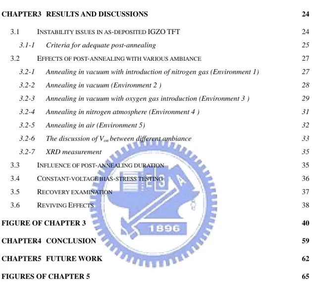
FIG.1.1OVERLAPPING OF S ORBITALS OF (N -1) D10NS0METALS IN AN M–O–M BOND, WHERE M DENOTES THE METAL.
8 FIG.1.2(A)SCHEMATIC ORBITAL DRAWING OF COVALENT SEMICONDUCTORS WITH SP3 ORBITALS.(B)SCHEMATIC ORBITAL
DRAWING POST-TRANSITION-METAL OXIDE SEMICONDUCTORS WITH METAL S ORBITALS [8]. 8
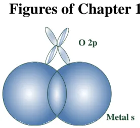
FIG.1.3SCHEMATIC ILLUSTRATION OF CONDUCTION AND ELECTRONIC STRUCTURE AROUND CONDUCTION BAND EDGE.THE ROUGH SURFACE REPRESENTS THE CONDUCTION BAND EDGE AND THE HORIZONTAL PLANE REPRESENTS THE FERMI LEVEL.AN ARROW IS AN ELECTRON CONDUCTION PATH.(A)AS THE FERMI LEVEL IS BELOW THE CONDUCTION BAND EDGE, NOT ENOUGH ELECTRONS WERE IN INDUCED.(B)WHILE THE FERMI LEVEL INCREASES, THE ELECTRONS DRIFT THROUGH THE POTENTIAL ENERGY BARRIERS.(C)WHEN THE FERMI LEVEL IS ABOVE THE CONDUCTION BAND EDGE, THE ELECTRON TRANSPORT IS CONTROLLED BY DEGENERATE MECHANISM [17]. 9
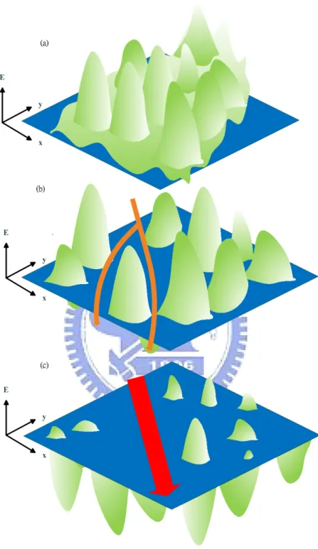
FIG.2.1SCHEMATIC CROSS-SECTION OF THE BOTTOM-GATE A-IGZOTFTS STRUCTURE. 22
FIG.2.2SKETCH OF LOW PRESSURE CHEMICAL VAPOR DEPOSITION (LPCVD). 22
FIG.2.3SCHEMATIC SKETCH OF RADIO-FREQUENCY -MAGNETRON SPUTTER. 23
FIG.3.1THE INSTABILITY OF THE AS-DEPOSITED IGZOTFT. 41
FIG.3.2DURING THE PREVIOUS IDVG MEASUREMENT, THE MOBILE CARRIERS WERE TRAPPED BY DEFECTS. 42 FIG.3.3LARGER POSITIVE GATE VOLTAGE WAS NEEDED TO TURN ON THE TRANSISTOR IN THE FOLLOWING MEASUREMENT 42
FIG.3.4STABILITY IMPROVEMENT BY POST-ANNEALING AT 350°C. 43
FIG.3.5THE EVOLUTION OF TURN-ON VOLTAGE OF FIG.3.4. 44
FIG.3.6THE EVOLUTION OF MOBILITY OF FIG.3.4. 44
FIG.3.7COMPARES THE TRANSFER CHARACTERISTICS OF (A) AS-FABRICATED A-IGZOTFT,(B) ANNEALED A-IGZOTFTS TREATED WITH FURNACE ANNEALING AT 300°C, AND (C) FURNACE ANNEALING AT 350°C. 45
FIG.3.8THE TRANSFER CHARACTERISTICS OF THE A-IGZOTFTS WHICH WERE ANNEALED AT TEMPERATURE RANGING FROM
300OC
TO 600OC FOR AN HOUR WITH THE ENVIRONMENT OF VACUUM WITH NITROGEN INTRODUCTION. 46
FIG.3.9THE TRANSFER CHARACTERISTICS OF THE A-IGZOTFTS WHICH WERE ANNEALED AT TEMPERATURE RANGING FROM
300OC
TO 600OC FOR AN HOUR IN VACUUM WITH THE FURNACE PRESSURE OF 3.5×10⁻⁷TORR. 47
FIG.3.10THE TRANSFER CHARACTERISTICS OF THE A-IGZOTFTS ANNEALED AT TEMPERATURE RANGING FROM 300OC TO
600OC
FOR AN HOUR WITH THE ENVIRONMENT OF VACUUM WITH OXYGEN INTRODUCTION. 48
FIG.3.11THE RELATIONSHIP BETWEEN TURN-ON VOLTAGE (VON) AND ANNEALING TEMPERATURE OF FIG.3.10. 49 FIG.3.12THE TRANSFER CHARACTERISTICS OF THE A-IGZOTFTS WHICH WERE ANNEALED AT TEMPERATURE RANGING
FROM 300OC TO 600OC FOR AN HOUR IN A NITROGEN ATMOSPHERE. 49
FIG.3.13THE TRANSFER CHARACTERISTICS OF THE A-IGZOTFTS WHICH WERE ANNEALED AT TEMPERATURE RANGING
FROM 300OC TO 600OC FOR AN HOUR IN AIR. 50
AMBIANCE. 51
FIG.3.15THE RELATIONSHIP BETWEEN THE TURN-ON VOLTAGE AND ANNEALING TEMPERATURE IN ATMOSPHERE BASED
AMBIANCE. 52
FIG.3.17THE TRANSFER CHARACTERISTICS OF THE A-IGZOTFTS ANNEALED AT THE TEMPERATURE OF 300OC FOR AN HOUR,300OC FOR TWO HOURS,400OC FOR AN HOUR, AND 400OC FOR 0.5 HOUR. 53
FIG.3.16THE XRD MEASUREMENT OF AS-DEPOSITED, ANNEALED AT 500OC, ANNEALED AT 600OC IN VACUUM, AND
ANNEALED AT 600OC IN AIR. 52
FIG.3.18THE TRANSFER CHARACTERISTICS MEASURED UNDER CONSTANT GATE BIAS STRESS OF 20V.A TEMPORAL INTERVAL OF 500 SECOND WAS BETWEEN TWO TRANSFER CURVE MEASUREMENTS. 54
FIG.3.19 SHOWS THE EVOLUTION OF (A) TURN-ON VOLTAGE (VON),(B) SUB-THRESHOLD SWING (S.S.), AND (C) MOBILITY
UNDER CONSTANT GATE BIAS STRESS OF 20V. 55
FIG.3.20THE TRANSFER CHARACTERISTICS OF RECOVERY EXAMINATION.A TEMPORAL INTERVAL OF 500 SECOND WAS
BETWEEN TWO TRANSFER CURVE MEASUREMENTS. 56
FIG.3.21THE EVOLUTIONS OF THE (A) TURN-ON VOLTAGE (VON),(B) THE SUB-THRESHOLD SWING (S.S), AND (C) THE
MOBILITY DURING THE RECOVERY EXAMINATIONS. 57
FIG.3.22THE REVIVING EFFECTS. 58
FIG.4.1OXYGEN ESCAPED AND FORMED OXYGEN VACANCIES IN THE A-IGZO FILM. 61
FIG.4.2THE OXYGEN IN THE AMBIANCE WAS INTRODUCED INTO THE A-IGZO FILM DURING ANNEALING AT HIGH
TEMPERATURE IN THE ENVIRONMENT WITH RELATIVELY HIGH OXYGEN CONCENTRATION. 61
FIG.5.1THE TDS SPECTRA FOR THE MASS FRAGMENTS (M/Z) OF 32 CORRESPOND TO THE OXYGEN MOLECULE. 65
FIG.5.2THE SURFACE CHEMISTRY OF THE ANNEALED A-IGZO FILMS USING XPS. 66
XI
Table Captions
TABLE 1.1GENERAL COMPARISON THROUGH A-SI:H, PENTACENE, AND A-IGZO BASED TFTS. 11
TABLE 3.1THE TYPICAL PARAMETERS OF FIG.3.1 41
TABLE 3.2THE TYPICAL PARAMETERS OF FIG.3.4 43
TABLE 3.3THE TYPICAL PARAMETERS OF FIG.3.8. 46
TABLE 3.4THE TYPICAL PARAMETERS OF FIG.3.9. 47
TABLE 3.5THE TYPICAL PARAMETERS OF FIG.3.10. 48
TABLE 3.6THE TYPICAL PARAMETERS OF FIG.3.12. 50
TABLE 3.7THE TYPICAL PARAMETERS OF FIG.3.13. 51
TABLE 3.8THE TYPICAL PARAMETERS OF FIG.3.17. 53
TABLE 3.9THE TYPICAL PARAMETERS OF FIG.3.18. 54
Chapter1
General Introduction
1.1 Introduction
Electronics devices fabricated on flexible substrates (flexible electronics) are emerging
rapidly in the research community and industry. Using the thin flexible substrates, some
flexible and mobile electronic products are developed. The roll-able displays, wearable
computers, and paper displays in the electronics market is expand rapidly. In the technology
of the flexible electronics, the process temperature of the transistor was limited due to the
limitation of the substrate temperature [1, 2].
Choosing the low temperature process was a main issue to develop the flexible electronics.
To execute the low temperature process, the choice of the depositing technologies and the
channel materials are the most important issue. A wide variety of different channel materials
have been investigated, such as organic semiconductors and hydrogenated amorphous silicon
(a-Si:H). However, in view of the inherent limitations of these materials, the development of
high-performance device must be carried out. The field-effect mobilities (
μ
eff) in a-Si:H TFTs are about ~1 cm2V-1s-1, and theμ
eff of a pentacene based OTFTs are around ~2.7 cm2V-1s-1 [3]. These values are still not appropriable for high-solution carrier injection devices. In addition,2
transparent device. Therefore, amorphous oxide materials with large-mobility that can be
fabricated at low temperatures have been considered for developing the display industry.
Metal oxide semiconductor was first reported in 1964 by H. A. Klasens et.al [4].In 1996,
novel oxide family of materials involving the use of multi-component combinations of
heavy-metal cations was reported by Hosono et al [5]. Over the past few years, several oxide
materials are reported to be the channel material in TFTs. The polycrtstalline zine oxide (ZnO)
[6,7], amorphous zinc tin oxide (ZTO) [8], amorphous zinc indium oxide (ZIO) [9], and
amorphous indium gallium zinc oxide (IGZO) [10-12]are proposed to be the active layer in
transparent TFTs. These amorphous oxide semiconductors (AOSs) have some unique
advantages, such as visible light transparency, large-area uniform deposition at low
temperature, and high carrier mobility. Among them, the high carrier mobility and stability are
the most attractive characteristics. The carrier mobility in AOS material is roughly ten times
larger than that of hydrogenated amorphous silicon (a-Si:H). Compare to the a-Si:H TFTs,
higher stability in AOS was demonstrated by Hung et al [13]. Among these AOSs, the
amorphous In-Ga-Zn-O (a-IGZO) has attracted a great deal of interest as TFTs material since
Hosono et al. reported high performance TFTs with the a-IGZO active layer deposited by
pulsed laser deposition (PLD) [10].They can easily exhibit relatively high mobilities ( >3
cm2V-1s-1), 1-2 V threshold voltage, current on/off 107-108, subthreshold slopes of 0.1-0.2 V
shows the general comparison through a-Si:H, pentacene, and a-IGZO based TFTs. These
excellent performances originate from the unique electron structure, the electron transport
path is very efficient because of the ns orbitals of these metal elements have large radii and
large overlap. However, many fundamental physical properties are still not well studied. In
this thesis, the effect of different ambient under post-annealing of a-IGZO will be carried out.
It is known that many fabrication process factors can affect TFT performance such as
post-annealing. Though a-IGZO can fabricate at room-temperature and present higher
performance than other materials, but it is still considered natural that a chemical species
and/or a structure is more stable at high temperatures and relaxes to a more stable structure
upon thermal annealing [16]. It is possible that post-annealing can decrease the number of
physical voids, traps, and/or defects within an active layer, although the intrinsic nature of
thermal annealing effect has yet to be clarified. Among the post-deposition thermal annealing
techniques, rapid thermal annealing (RTA), laser annealing, furnace annealing or other
techniques are used in TFT devices. In this thesis, furnace annealing is chosen to observe the
effects of thermal annealing in various annealing ambients.
1.2 The mechanisms of a-IGZO Thin film Transistors
As described in the previous section, a-IGZO exhibit interesting and attractive properties
4
1.2-1 Small electron effective mass [17]
Their conduction band minimum (CBM) is mainly composed of vacant s-orbitals of a
metal cation and valence band maximum (VBM) is of oxygen 2p-orbitals [18]. For IGZO,
CBMs are composed of s orbitals with a large principle quantum number n (n =5 for In).
These s orbitals have large spatial size and form direct overlap between the neighboring metal
cations, as showed in Figure 1.1. Since electron conductivity is represent as
(1.1)
where n is the carrier density and μ is the mobility. Thus, the mobility is inversely
proportional to the carrier effective mass, m*,
, (1.2)
where < > is the mean time between scattering events, and q is the electron charge [19]. From
the formula of one-dimensional lattice in k-space
E = Hnn + 2Hmncos(ka) Hnn + 2Hmn – Hmn(ka)2 , (1.3)
where a is the lattice constant, and Hmn is the Hamiltonian matrix element,which is expressed
as Hmn = *(xm)H (xm)dx and is stand for the magnitude of the interaction between two
orbitals from different atoms, where is the electron orbital [20]. Due to the effective mass
of the electron is described as
m* = , (1.4)
m* , (1.5)
Since Hmn in Eq. 1.5 represents the magnitude of the interaction between two overlapping
orbitals of different atoms. Thus, this is the reason why a-IGZO have small electron effective
masses of 0.23-0.35me [21], where me is the mass of a free electron. Finally, Eq. 1.2 results in
a larger mobility.
1.2-2 Unique chemical bonding
Usually, amorphous semiconductors exhibit low mobility as known in a-Si:H. It is
because the carrier transport is controlled by hopping between localized tail-states and
conduction band. The intrinsic nature of the chemical bonding is consist of sp3 orbitals with
strong spatial directivity. In this case, the magnitude of the overlap between the vacant
orbitals of the neighboring atoms is very sensitive to the variation in the bond angle. It
indicates that a-Si:H are characterized by low mobilities. In contrast, the ionic bonding
structure of a-IGZO with a large principle quantum number, where n = 5, consists of large
radii s-orbitals cations, which are isotropic shape and their overlaps with neighboring metal s
orbitals remain almost unaltered compared to that of a crystalline structure, as illustrated in
Fig. 1.2 [10]. Fig. 1.2(a) shows the schematic orbital drawing of covalent semiconductors
with sp3 orbitals. Fig. 1.2(b) shows the schematic orbital drawing of post-transition-metal
oxide semiconductors with metal s orbitals.
6
Another characteristic of a-IGZO which is different from conventional crystalline
semiconductors, such as Si, is their Hall mobility increases with the increasing of the carrier
concentration. Since the carrier mobility of Si decrease with increasing the carrier
concentration owing to ionized impurity scattering in highly doped materials. It was found
that IGZO film exhibits extremely high mobility compared with the silicon based materials.
Nomura et al. reported that the carrier transport in crystalline oxide semiconductor
InGaO3(ZnO)5 using single-crystalline thin films [22]. Percolation conduction was observed
when carrier concentrations (Ne) were lower than a definite Nth, and it changes to degenerate
conduction at Ne > Nth. Nomura et al. speculated a similar carrier transport behavior in
a-IGZO [23]. They suggested that percolation conduction through the distribution of the
potential barrier around the conduction band edge for a-IGZO. According to this model shows
in Fig. 1.3 [17,24], when the Fermi level is below the highest energy barriers, the electrons
drift through the potential energy barriers. Once the Fermi level is above these conduction
band potential energy peaks, the electron transport is controlled by degenerate mechanism and
will possible obtain large mobility in randomness structure.
1.2-4 Tunable carrier concentration
Substitutional doping is not a efficient way for crystalline semiconductors and a-Si:H.
Though, it is really effective. In contrast, for IGZO film, it is very easy to alter the
process. It is an effective doping way to inject the carrier electrons to the CBM [24].
1.2-5 Composition of a-IGZO
IGZO is a composite of In2O3, Ga2O3 and ZnO. It is clarified that the mobility is primary
determined by the fraction of In2O3 content due to its tendency to form oxygen vacancies. To
suppress oxygen vacancy creation, the addition of an oxide with a strong metal-oxygen bond
is required. It is demonstrate that incorporation of Ga3+ is very effective for suppressing
oxygen vacancy creation[24]. Finally, ZnO is formed by a small atomic distance between Zn
atoms, which increases the conduction band minimum (CBM) and leads to an increase in the
electron mobility [25]. Therefore, InGaZnO4 is chose as the channel layer of the TFT for this
thesis.
1.3 Motivation
As mentioned above, thermal annealing is essentially important for fabricating a-IGZO
TFTs. However, the ambient gas for thermal annealing can also influence device
characteristics seriously. Up to date, few studies [26] had focused on the ambient issues
during the process of thermal annealing. Whereas the behaviors of a-IGZO in different
ambient for thermal annealing is quite interesting. In this thesis, the analysis in various
8
Figures of Chapter 1
Metal s O 2p
Fig. 1.1 Overlapping of s orbitals of (n - 1) d10ns0 metals in an M – O – M bond, where M
denotes the metal.
a. Covalent semiconductors, for example, silicon
b. Post-transition-metal oxide semiconductors
Fig. 1.2 (a) Schematic orbital drawing of covalent semiconductors with sp3 orbitals. (b)
Schematic orbital drawing post-transition-metal oxide semiconductors with metal s
Fig. 1.3 Schematic illustration of conduction and electronic structure around conduction band
edge. The rough surface represents the conduction band edge and the horizontal
plane represents the Fermi level. An arrow is an electron conduction path. (a) As the
10
induced. (b) While the Fermi level increases, the electrons drift through the
potential energy barriers. (c) When the Fermi level is above the conduction band
Table 1.1 Gener al
comparison through a-Si:H, pentacene, and a-IGZO based TFTs.
Material μ (cm2
/V s) Vth (V) Crystalline Temp.
IGZO 3~100 -1-~10 No ≧RT
a-Si:H ≦1 1~6 No ≦150℃
12
Chapter2
Experimental Procedure
2.1 Device structures and fabrication
Heavily doped p-type Si (100) was used as a substrate and a gate electrode. Figure 2.1
shows a schematic cross-section of the bottom-gate a-IGZO TFTs structure used in this study.
The detail fabrication process including dielectric deposition, a-IGZO film deposition,
source/drain deposition and post-annealing are described in the following sections.
2.1-1
Dielectric deposition
The dielectric silicon nitride (SiNx) was formed on all samples with 1000Å using low
pressure chemical vapor deposition (LPCVD) as showed in Figure 2.2. The SiNx was
deposited in high temperature of 780°C. The reactant gas of NH3 and SiH2Cl2 were introduced
to form the Si3N4 film:
3 SiH2Cl2 + 4 NH3 → Si3N4 + 6 HCl + 6 H2
Before depositing the active layer, the standard clean was carried out to remove the
contamination on the dielectric surface. The standard clean is accomplished in two steps, SC1
and SC2. SC1 clean is the first step to remove the particle on the surface. The process was
executed with a mixture of ammonium hydroxide, an oxidant hydrogen peroxide, and water in
a mixing ratio of 1:4:20.
The SC2 clean was used to remove metals from the surface. The cleaning process in SC2
contain three solutions of HCl , hydrogen peroxide, and water. The mixture ratio in the SC2
process was 1:1:6:
HCl : H2O2: H2O = 1:1:6(SC2)
2.1-2 a-IGZO film deposition
Generally, pulsed laser deposition (PLD) and radio frequency (RF) -magnetron sputter
were reported to deposit a-IGZO film as channel layer [10,12]. In this study, the rf-sputter
with the 6-in. circular target: In2O3:Ga2O3:ZnO = 1:1:1 at.% was used to deposit the a-IGZO
film. 70nm a-IGZO channel layer was deposited at room temperature with a power of 300W,
a working pressure of 3.75 mTorr, and an O2/Ar flow rate of 0/20. The active layer patterning
was defined using a shadow mask.
[27] RF sputtering (Fig. 2.3) is a process using radio frequency power supply, operating
at 13.56 MHz, to generate plasma in which atoms, ions, and clusters are created to sputter the
target material. The glow-discharge between a target and a substrate, it is consists of plasma
with an equal number of working gas ions (Ar) and electrons. The ions are accelerated
towards to the target by a strong electric field on the target due to the flux of electrons.
Consequently, the ions hit the target to eject the target atoms, which are then re-deposited onto
the substrate. RF sputtering is performed at low pressure, to increase the mean free path, the
14
2.1-3 Source/Drain deposition
Several candidate metallic electrodes were reported for amorphous oxide semiconductor.
[28] Y. Shimura et al. proposed that the electrode of titanium (Ti) used in a-IGZO TFT shows
excellent performance. The metal in source/drain contacts was deposited using electron beam
(E-beam) evaporation. The mechanism in E-beam evaporation was using an electron beam to
heat a source of material in a crucible. The electrons are emitted from a heated filament to hit
the source in a high velocity of several kV. The base pressure of the E-beam evaporator is
4x10⁻⁶ torr, and 1000 nm-thick titanium (Ti) pads were deposited through a shadow mask.
Finally, as presented in the Figure 2.1, the channel length (L) is 400 um and the channel width
(W) is 1000 um for the fabricated a-IGZO TFT.
2.1-4 Post-annealing
After deposition of the electrodes, post-annealing is carried out in the furnace. In the
series of the experiments, different conditions are used. For the vacuum condition, the
working pressure is 3.5×10⁻⁷ torr. With the annealing process in a nitrogen (N2) rich term, the
base pressure is 3.5×10⁻⁷ torr, and the furnace is operated at a total pressure of 3×10⁻¹ torr and
at a N2 flow rate of 120 standard-cubic-centimeter-per-minute (sccm). As the annealing
process in an oxygen (O2) rich term, the base pressure is 3.5×10⁻⁷ torr, and the furnace is
operated at a total pressure of 3×10⁻¹ torr and at a O2 flow rate of 120
the base pressure is atmospheric pressure, and the N2 flow rate is 10 liter per minute (L/min).
The annealing temperature was varied from 300oC to 600oC to observe the post-annealing
effect of the a-IGZO TFTs.
2.2 Analysis instruments
2.2-1 X-ray photoelectron spectroscopy (XPS)
[29] X-ray photoelectron spectroscopy (XPS), also called electron spectroscopy for
chemical analysis (ESCA), is a electron spectroscopic method that measures the elemental
composition, empirical formula, chemical state and electronic state of the elements that exist
within a material. The phenomenon is based on the photoelectric effect outlined by Einstein in
1905. The XPS spectra can be analyzed by exposing a beam of X-rays on a material surface.
The surface chemistry was characterized by measuring the kinetic energy (EK) and the
number of electrons escaped from the surface of the material while the X-rays exposing.
The electron binding energy (BE) of each emitted electrons can be convinced by using
the equation,
Ebinding = Ephoton – (Ekinetic+ ψ) (2 . 1 )
where Ebinding is the electron binding energy, Ephoton is the energy of the X-ray photons, Ekinetic
is the measured electron kinetic energy and φ is the work function of the spectrometer. The binding energy of the peaks is unique for each element and the peak areas can be used to
16
analyze the composition of the materials surface. The major strength of XPS is that it allows
chemical and elemental identification due to the electron binding energy can be influenced by
its chemical surroundings making Ebinding proper to determine chemical states [29].
2.2-2 Thermal desorption spectrometry (TDS)
[30] Thermal desorption spectroscopy (TDS) is used to observe the desorbed molecules
from a film when the temperature is increased. When molecules contact with the surface, they
adsorb onto it and form a chemical bond with the surface to minimize their energy. Three
forms for molecules desorbed from the surface were reported. [30] Direct desorption,
dissociative desorption, and associative desorption were the main desorption mechanisms. For
direct desorption, desorbed molecules remain the same chemical structure as the molecules on
the surface. When the desorbed molecules dissociate to smaller molecules, it is called
dissociative desorption. If the desorbed molecule composed with more than two elements, the
desorbed process is related to the associative desorption. A mass spectrometer is used to
measure desorption molecules. The desorbed molecules and the desorbing temperatures of
molecules were measured and analyzed by the TDS. The quantity of adsorbed molecules on
the surface from the intensity of the peaks in TDS spectrum, and the integral of the spectrum
can also show the total amount of adsorbed species [30].
[29] X-ray diffraction is a non-destructive technique for determining crystallographic
structure of materials and thin films. It is based on observing the scattered intensity of an
X-ray beam which is exposed on sample as a function of incident and scattered angle.
Consider a monochromatic X-ray beam with wavelength λ incident on a sample at an angle θ, the primary beam is transmitted through the sample. The diffraction occurs only when the distance traveled by the rays was twice to the rays reflected from planes at the fixed
Bragg angle θB,
θB = arcsin (λ/2d) (2.2)
where d is the lattice planes space. XRD plot is produced by the angular positions and
intensities of the resultant diffracted peaks of radiation, which reveals the own specific
18
2.3 Methods of device parameters extraction
In this section, the extractions of the device parameters are discussed in details. The
turn-on voltage (Von), the on/off current ratio (Ion/Ioff), the sub-threshold swing (S), and the
field effect mobility are extracted and assessed, respectively.
2.3-1 Mobility
[29] Mobility is a measurement of the velocity of the carriers move through a material. A
higher mobility allows for higher frequency response such as the time it takes for the device
to transform from the off state to the on state. In the off state, few current flows through the
device. In the on state, large amount of currents flow through the device. A larger mobility
value means that the device can conduct more current.
The mobility in this study was extracted from the saturation region of the transfer
characteristic. The device was operated at the drain-voltage of 20 V, since the threshold
voltage was much lower than 20 V. The saturation mobility is determined from the
transconductance, defined by
(2.3)
(2.4) When the mobility is determined, the transconductance is usually taken to be
(2.5)
When this expression is solved for the mobility, it is known as the saturation mobility
(2.6)
2.3-2 On/off current ratio (I
on/I
off)
The on/off current ratio in TFTs LCD determines the gray-level switching of the displays.
High Ion/Ioff means the on current was high enough to drive the pixel and the off current was
low enough to keep in low power consumption. It was obtained by plotting the log(ID) versus
VGS at a large VDS of 20 V. A large on/off current is required for certain switching applications,
and it is desire to be larger than 106. The off current represents how much power is lost when
the device is off. The on current shows the maximum current drive for the device.
2.3-3 Sub-threshold swing (S.S.)
[31] Sub-threshold swing is also an important characteristic for device application. It is a
20
exponential current increase. The reciprocal of the slope of the log(ID) versus VGS
characteristic is defined as the sub-threshold swing (S).
(2.7)
If we want to have good performance TFTs, we need to lower the sub-threshold swing (S) of
transistors.
2.3-4 Turn-on voltage (V
on)
Turn-on voltage (Von) is identified as the gate voltage at which the drain current
begins to increase in a transfer curve. Von can directly characterizes the gate voltage required
to fully ‘‘turn off’’ the transistor in a switching application. [32] To observe the shift in the
transfer curve, Von was chosen instead of threshold voltage (Vth). Threshold voltage was
extracted ambiguity within many thin-film transistors due to the fundamental conflict in the
drain current equation. The value of the Vth extracted by everyone may be different in the
same device. To confirm the stability precisely in the transfer curve, the Von was proposed to
compare the stability of the a-IGZO device.
2.3-5 Threshold voltage (V
th)
Threshold voltage is related to the operation voltage and power consumptions of TFTs.
We extract the threshold voltage from equation (2-5), the intercept point of the square-root of
22
Figures of Chapter 2
Heavily-doped Si substrate
SiN
XIGZO
Ti
Ti
120 nm 70 nm 100 nm W/L = 1000 mm/ 400 mmFig. 2.1 Schematic cross-section of the bottom-gate a-IGZO TFTs structure.
heater
H2/N2 wafer
Ground Vacuum Sputtering gas inlet
Heater Electrode Wafer Argon plasma Electrode/Target Match network RF Generator RF Input
24
Chapter3
Results and Discussions
3.1 Instability issues in as-deposited IGZO TFT
[16, 33] H. Hosono et al. proposed that the chemical species and/or a structure in the
metal oxide channel layer of a transistor are naturally unstable when thin the film was
deposited at low temperatures. On the contrary, they are relatively stable while thin films are
deposited at higher temperatures [16]. The chemical species and/or structure of a metal oxide
channel layer lead to an unstable electric characteristics of transistor. It has been generally
demonstrated that post-thermal annealing could make metal oxide transistor stable.
Figure 3.1 presents the instability of the as-deposited IGZO TFT. Exemplary drain current
versus gate voltage (IDS-VGS) curve measurement was carried out at room temperature in air.
The transfer curve proceeded with constant VDS of 20 V and VGS ranging from -15 V to 20 V.
It was seen that the transfer curve shift to higher gate voltage direction with sequent IDVG
measurement. The turn-on voltage shift of approximately 11.5 V was achieved after seven
times sequent IDVG measurement (Von= 2.4V (first curve), Von= 13.9 V (seventh curve). Table
3.1 lists the typical parameters such as mobility, turn-on voltage, threshold voltage, Ion/Ioff
current ratio, and sub-threshold swing.
formed in the interface between channel and dielectric layer. The mechanism was considered
that the atomic bonding of film was loose due to low temperature during sputter process.
Loose structure means the defects. It was assumed that during the previous IDVG measurement,
the mobile carriers were trapped by defects, as showed in figure 3.2. Therefore, larger positive
gate voltage was needed to turn on the transistor in the following measurement, as showed in
figure 3.3. Besides, the mobility of the IGZO TFT also increased with the sequent
measurement. The coincidence between turn-on voltage shift and mobility may be caused by
the occupied defect state that could not trap or scatter mobile electrons anymore.
Stabilityimprovement by post-annealing at 350 °C was shown in Figure 3.4. Almost no
fluctuation in Von was observed during seven times sequent IDVG measurement. Table 3.2lists
the typical parameters such as mobility, turn-on voltage, threshold voltage, Ion/Ioff current ratio,
and sub-threshold swing. Figure 3.5 and figure 3.6show the evolution of turn-on voltage and
the evolution of mobility respectively. The influence of annealing on on-voltage and mobility
were presented. It was believed that post-annealing could decrease the defect states near
channel/dielectric interface. Maybe it’s because high-temperature could realign the atoms in
IGZO film and make structure more order [16]
3.1-1 Criteria for adequate post-annealing
Figure 3.7 compares the transfer characteristics of as-fabricated a-IGZO TFT, annealed
26
3.7(a) presents sequent transfer curves of the as-deposited a-IGZO TFT, the serious
divergence of transfer curves reflect that the as-fabricated a-IGZO TFT was unstable. After
seven times sequent IDVG curve measurements, the transfer curve shifted from 2.4 V to 13.9 V.
The turn-on voltage will achieve saturation within seven times sequent measurement.
Compare to the as-deposited a-IGZO TFT, the a-IGZO TFT treated with furnace annealing at
300°C performs more stable. The sequent transfer curves of the 300°C annealed a-IGZO TFT
is shown in Fig. 3.7(b). We judge the stability of 300°C annealed a-IGZO TFT is still
inadequate because the negligible turn-on voltage shifts of 1.7 V during seven times sequent
measurements. All the IDVG curve measurement in this study proceeded with a constant drain
voltage of 20V. Fig. 3.7(c) shows the transfer characteristics of a-IGZO TFT treated with
furnace annealing at 350°C. Apparently, the transfer curves of 350°C furnace annealed
a-IGZO TFT kept almost constant during seven times sequent measurements. Hence, it is
believed that the optimal post-annealing condition is temperature dependent.
As shown in figure 3.7, the turn-on voltage of transfer curve will achieve saturation
within seven times sequent measurement for a-IGZO TFTs , whether the TFT was treated with
annealing or not. Therefore, seven times sequent measurement was executed for all a-IGZO
TFTs to reflect the stability. In this study, we grade the instability by the turn-on voltage shift
(△Von). △Von is the difference between the turn-on voltage of the first and seventh IDVG
△Von = Von (7) – Von (1)
3.2 Effects of post-annealing with various ambiance
The result in last section demonstrates that post-annealing is an indispensable process for
the employed IGZO TFTs in this study to get adequate stability. In this thesis, optimized
post-annealing condition was found out by a series of experiment. Besides, the effect of the
environment during furnace annealing on a-IGZO TFTs was also clarified. The destination of
this study is to provide a guideline to research the optimal annealing condition for
as-fabricated a-IGZO TFTs.
3.2-1 Annealing in vacuum with introduction of nitrogen gas
(Environment 1)
Figure 3.8 shows the transfer characteristics of the a-IGZO TFTs which were annealed at
temperature ranging from 300oC to 600oC for an hour. The base pressure of furnace is
3.5×10⁻⁷ torr. During annealing, nitrogen gas was introduced into furnace with flow rate of
120 standard-cubic-centimeter-per-minute (sccm) and the furnace pressure maintained the
value of 3×10⁻¹ torr. Table 3.3 lists the typical parameters such as mobility, turn-on voltage, on
voltage shift (△Von), threshold voltage, Ion/Ioff current ratio, and sub-threshold swing (S.S.).
It is obvious that the off-current (Ioff) increased significantly with increasing annealing
28
a-IGZO TFT was treated by annealing at temperature of 400oC, the TFT will lose its
adjustability of current due to high conductive IGZO channel. When the annealing
temperature further increased to 500oC, the drain current (ID) will not be modified anymore by
gate voltage. The drain current maintained a constant value of 4.9×10⁻⁴A during VG sweeping.
This could be explained by that the oxygen components near the a-IGZO surface were
pumped away during annealing at a relatively high temperature in a vacuum furnace. Oxygen
escaped and formed oxygen vacancies in the a-IGZO film, and oxygen vacancy is an accepted
electron dopant in metal oxide material. Therefore high temperature annealing could induce
high carrier concentration and make IGZO film conductive.
As shown in figure 3.8, the transfer characteristics of the a-IGZO TFT annealed at 300oC
present well adjustability of current. The extracted field effective mobility and sub-threshold
swing are 6.47 cm2/Vs and 0.13 V/decade respectively. However, the turn-on voltage still
shifted 3.7 V during seven times sequent measurement. In other words, the a-IGZO TFTs
treated with 300℃ annealing is inadequately stable.
3.2-2 Annealing in vacuum (Environment 2 )
Figure 3.9 showsthe transfer characteristics of the a-IGZO TFTs which were annealed at
temperature ranging from 300oC to 600oC for an hour in vacuum with the furnace pressure of
3.5×10⁻⁷ torr. Table 3.4 lists the typical parameters such as mobility, turn-on voltage, turn on
The trend of the experiment result is similar to the one with annealing environment of
vacuum with nitrogen introduction (environment 1) that has been mentioned in section 3.3-1.
The conductivity increases with annealing temperature. However, the slope of
conductivity-temperature curve is relatively smaller in contrast with the one with environment
1. Obviously, the oxygen molecule density of environment of vacuum (environment 2) was
less than environment 1. Thus, the forming of oxygen vacancies in IGZO during annealing at
high temperature with environment 1 is relatively difficult as compared with the one with
environment 2. Table 3.4 lists the extracted parameters of transfer characteristic of a-IGZO
TFT annealed at 350oC. The turn-on voltage (Von), sub-threshold swing (S.S.), and on/off
current ratio are 0.6 V, 0.34 V/decade and > 107, respectively. The turn-on voltage shift (△Von)
of 0.3 V was achieved during seven times sequent transfer curve measurement with a constant
drain voltage of 20 V. As shown in figures 3.8 and 3.9, it indicates that the a-IGZO TFTs
annealed at 350℃ in condition 1 and condition 2 perform well electric characteristic with
both adequate stability and performance as compared with the ones annealed at different
temperatures.
3.2-3 Annealing in vacuum with oxygen gas introduction
(Environment 3 )
Figure 3.10 shows the transfer characteristics of the a-IGZO TFTs annealed at
30
oxygen introduction. The base pressure of 3.5×10⁻⁷ torr was achieved at first, then oxygen gas
was introduced into the furnace with a flow rate of 120 sccm. Finally the furnace pressure of
3×10⁻¹ torr was maintained during annealing process. Table 3.5lists the typical parameters
extracted from the data in figure 3.10, such as mobility, turn-on voltage (Von), turn-on voltage
shift (△Von), threshold voltage, Ion/Ioff current ratio, and sub-threshold swing (S.S.).
Electric characteristics of the a-IGZO TFT with annealing environment of vacuum with
oxygen introduction (environment 3) are roughly similar to the ones with annealing
environment of vacuum (environment 2) and vacuum with nitrogen introduction (environment
1). The conductivity of IGZO channel increased with annealing temperature. In detail, the
feasible range of annealing temperate is wider as compared with the ones of environment 1
and environment 2. Table 3.5shows that the Von of transfer curve of IGZO TFTs annealed at
400oC and 450oC were only 0.1 V and 0 V respectively. Compare a-IGZO TFT annealed in
environment 1, environment 2 and environment 3, it presents that the concentration of oxygen
molecules in post-annealing ambiance plays an important role. The final concentration of
oxygen vacancies in IGZO layer annealed at high temperature depends on the ambient oxygen
concentration. Oxygen vacancy is an accepted mobile electron dopant in metal oxide
semiconductor. Figure 3.11 shows the relationship between turn-on voltage (Von) and
annealing temperature. Von decreases with increasing temperature and reached -1.55 V at
as shown in Figure 3.8, Figure 3.9, and Figure 3.10.
3.2-4 Annealing in nitrogen atmosphere (Environment 4 )
Figure 3.11shows the transfer characteristics of the a-IGZO TFTs which were annealed
at temperature ranging from 300oC to 600oC for an hour in a nitrogen atmosphere (condition
4). At first the furnace was filled with air, then nitrogen gas was continuously introduced into
furnace with a flow rate of 10 liter per minute (L/min). The nitrogen flow rate was maintained
during the whole annealing process. Table 3.6 lists the typical parameters such as mobility,
turn-on voltage, turn-on voltage shift (△Von), threshold voltage , Ion/Ioff current ratio, and
sub-threshold swing (S.S.).
The oxygen content in nitrogen atmosphere during annealing process was relatively rich
in comparison to the one in environments 1, 2 and 3. As shown in figure 3.12, the evolution of
transfer curve with annealing temperature is opposite to the ones observed in previous
sections. The off-current (Ioff) of the transfer curve of a-IGZO TFTs annealed in nitrogen
atmosphere kept constant with increasing temperature. On the contrary, the on-current (Ion)
decreased with annealing temperature. There was one order decrease in the on-current of
500oC annealed a-IGZO TFT. As the a-IGZO TFT was treated with further high temperature
of 600oC, the TFT entirely lost its adjustability of current. The a-IGZO TFT presents insulator
behaviors that maintain a low current of 10-12 A during gate voltage sweeping. Specially, the
32
temperature. As mentioned above, the oxygen component near the a-IGZO surface were
pumped away during annealing at high temperature in a vacuum environment with relatively
low oxygen concentration. On the contrary, the oxygen in the ambiance was introduced into
the a-IGZO film during annealing at high temperature in the environment with relatively high
oxygen concentration. Table 3.6 presents that the a-IGZO TFTs annealed at temperature
ranging from 350oC to 500oC in nitrogen atmosphere were adequately stable. And it also
shows that the turn-on voltage (Von) shifted to negative direction with increasing temperature.
3.2-5 Annealing in air (Environment 5)
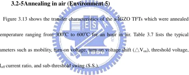
Figure 3.13shows the transfer characteristics of the a-IGZO TFTs which were annealed
at temperature ranging from 300oC to 600oC for an hour in air. Table 3.7 lists the typical
parameters such as mobility, turn-on voltage, turn-on voltage shift (△Von), threshold voltage,
Ion/Ioff current ratio, and sub-threshold swing (S.S.).
The trend of the transfer curve with increasing annealing temperature was similar to the
one with annealing environment of nitrogen atmosphere (environment 4). The phase of
a-IGZO channel tended to insulator with increasing temperature. The IGZO channel annealed
in air started to become an insulator at a lower turning temperature of 500oC as compared
with the one annealed in nitrogen atmosphere. It demonstrates that the concentration of
oxygen in post-annealing ambiance influences the electric characteristic of a-IGZO TFT
IGZO film during annealing process. Numerical variation of oxygen vacancy changes the
carrier concentration in the a-IGZO layer during the annealing process and cause varied
electrical characteristics. Table 3.7 presents that a-IGZO TFTs annealed in air at the
temperature ranging from 350oC to 400oC performed well compared to the one annealed at
temperatures exceeded this temperature range. Similar to other annealing environment
mentioned above, the turn-on voltage shifted to negative direction with increasing annealing
temperature.
3.2-6 The discussion of V
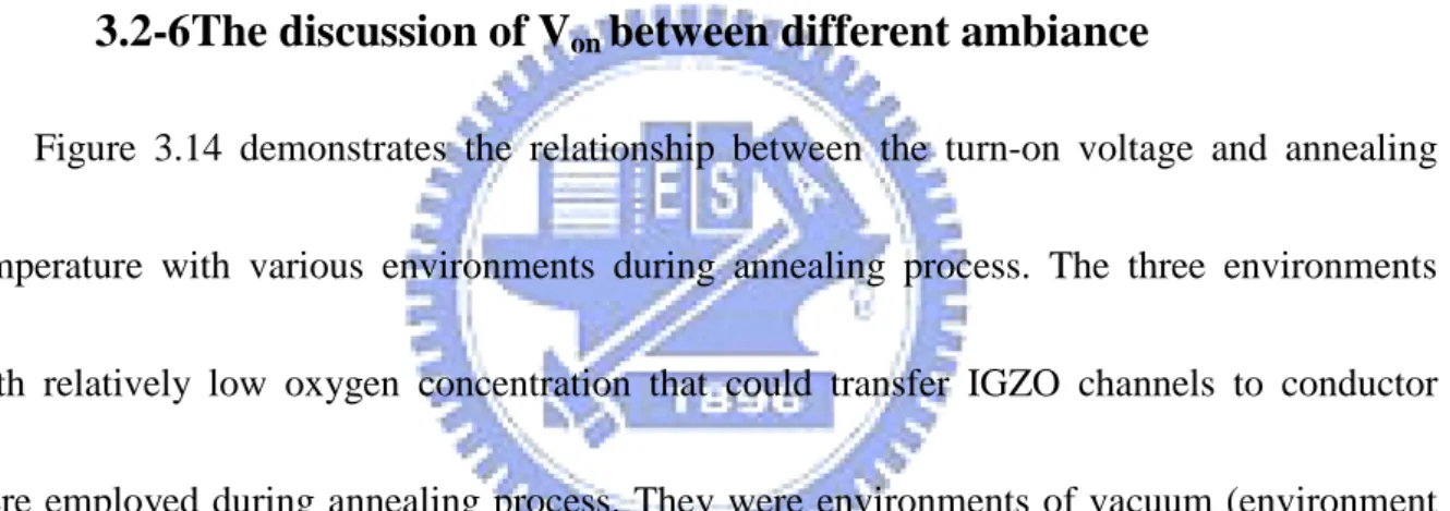
onbetween different ambiance
Figure 3.14 demonstrates the relationship between the turn-on voltage and annealing
temperature with various environments during annealing process. The three environments
with relatively low oxygen concentration that could transfer IGZO channels to conductor
were employed during annealing process. They were environments of vacuum (environment
2), vacuum with oxygen introduction (environment3) and vacuum with nitrogen introduction
(environment 1) mentioned above. The turn-on voltage shifted negatively as the temperature
increased in all annealing environment. It is thought that the oxygen component near the
a-IGZO surface could receive enough energy at high temperature to escape from the surface
and then create oxygen vacancies in the a-IGZO film. Since oxygen vacancy is accepted
electron dopant in metal oxide material and higher annealing temperature release more
34
turn on voltage means the intrinsically more mobile carrier concentration. Figure 3.15 shows
the relationship between the turn-on voltage and annealing temperature with various
environments during annealing process. The two environments with relatively high oxygen
concentration that could transfer IGZO channels to insulator were employed during annealing
process. They were environments of nitrogen atmosphere (environment 4) and air
(environment 5) mentioned above. Compared to the annealing environments with relative low
oxygen concentration (environments 1, 2 and 3), the trend of the turn-on voltage is similar
although the variation is smaller. It could be explained by the reduction of aceptor-like surface
states with increase annealing temperature. The effect of reducing aceptor-like surface states
contradicts the effect of reducing intrinsic carrier concentration. On other hand, reducing
aceptor-like surface states make negative Von shift, and reducing intrinsic carrier
concentration make positive Von shift. As a result, the effect of aceptor-like surface states is
dominant.
Figure 3.14 presents the evolution of Von of IGZO TFTs annealed in environments with
relatively low oxygen concentration. The Von belong to environment with higher oxygen
concentration is larger under an annealing temperature. It could be thought that there are two
reactions was proceeding during post-annealing, oxygen evaporation from IGZO film and
oxygen oxidation from environment. The oxygen oxidation is mainly dependent on oxygen
higher oxidation that reduce the intrinsic carrier concentration and lead to larger Von.
3.2-7 XRD measurement
The IGZO film was not crystallized until annealed at 600oC in both vacuumed based and
atmosphere based furnace, as showed in Fig. 3.16. Therefore, the devices annealed at 500oC
in vacuumed based ambiance were all conductive. According to this result, it was confirmed
that the conductive phenomenon was not caused by crystallization. Thus, it was believed that
the conducted and insulated phenomenon was controlled by oxygen vacancies.
3.3 Influence of post-annealing duration
As showed in table 3.6, a-IGZO TFT annealed in nitrogen atmosphere (environment 4) at
300oC for an hour was still unstable. The 2 V threshold voltage shift achieved within seven
times sequent IDVG measurements. Thus, we were motivated to confirm whether the
prolonged duration could improve the stability of a-IGZO TFTs. Besides, although a-IGZO
TFT annealed in nitrogen atmosphere at 400oC for an hour performed stable, the mobility was
relatively lower. Therefore, it was also motivational to confirm whether shortening the
annealing duration could improve the mobility without degrading the stability of a-IGZO
TFT.
Figure 3.17 shows the transfer characteristics of the a-IGZO TFTs annealed at the
36
hour. Table 3.8lists the typical parameters such as mobility, turn-on voltage, turn-on voltage
shift ( △ Von), threshold voltage , Ion/Ioff current ratio, and sub-threshold swing (S.S.).
Annealing in nitrogen atmosphere at 300oC for a prolonged duration of two hours improved
the stability that coincide with the expectation. However, the improvement was still
inadequate due to the negligible turn-on voltage shift (△Von) of 1 V. Annealing in nitrogen
atmosphere at 400oC for a shortened duration of 0.5 hour improved the mobility. However,
the device was relatively unstable as compared with the one with duration time of 1 hour. The
turn-on voltage shift could achieve 0.5 V during sequent IDVG measurement although the high
mobility of 5.36 cm2/Vs.
Depend on the experiment result presented above, it is difficult to make a-IGZO TFT
adequately stable if the annealing temperature is inadequate. Prolonging annealing duration
not only improve stability the but also degrade the mobility, the appropriate duration was
determined by making a trade-off.
3.4 Constant-voltage bias-stress testing
In this section, the result of bias-stress measurement with a constant gate voltage was
presented. Among the a-IGZO TFTs investigated in this study, the ones annealed in nitrogen
atmosphere at 350oC shows relatively excellent performance, therefore it was chose to
room temperature, in air and in the dark.
Figure 3.18shows the device’s transfer characteristics measured under constant gate bias
stress of 20V. There was a temporal interval of 500 second between two transfer curve
measurements. Eight transfer curves were probed during the whole process of bias stress
measurement. As shown in Fig. 3.18, the transfer curves of stressed and un-stressed IGZO
TFT were similar with each other. However, the transfer curve shifted to positive direction of
gate voltage under continuous bias stress. It may be the result from trapped negative carrier on
the channel/dielectric interface or injected charge in gate dielectric [28]. Table 3.9shows the
extracted typical parameters such as mobility, turn-on voltage, turn-on voltage shift (△Von),
threshold voltage, Ion/Ioff current ratio, and sub-threshold swing (S.S.). Sub-threshold swing
(S.S.) kept nearly constant during the examination of bias stress. This could be explained by
that there were no additional defect states created near channel/dielectric interface during bias
stress [28]. Fig. 3.19 shows the evolution of turn-on voltage (Von), sub-threshold swing (S.S.),
and mobility under constant gate bias stress of 20V.
3.5 Recovery examination
After the bias stress examination, the device was subjected following recovery
examination. The sequent transfer curves were measured with an idly period of 500 seconds
38
500 seconds latter after the ending of bias stress process, the first transfer curve was probed.
The threshold voltage recovered dramatically within 500s idle times. The first recovery curve
is an approximately exponential decay function with a decay constant of
500s, τ
t initial idle V e
V =∆ −
∆ , △Vinitial is the turn-on voltage shift after bias stress, τ is the decay constant, t is the idle time after bias stress, △Vidle is the turn-on voltage at the time of t. Table
3.10 shows the typical parameters such as mobility, on voltage, Von shift (△Von), threshold
voltage, Ion/Ioff current ratio, and sub-threshold swing (S.S).
Obviously, after the bias stress process, the turn-on voltage (Von) dramatically shifted
back with a distance of 2 V within 500 seconds. After the fourth IDVG measurement, the Von
almost recovered to the initial value before bias stress. During the idle phase, the recovery
phenomenon maybe due to the electron de-trapping from the interface or dielectric layers to
the active layers [29]. Figs. 3.21(a), 3.21(b), and 3.21(c) show the evolutions of the turn-on
voltage (Von), the sub-threshold swing (S.S), and the mobility during the recovery
examinations.
3.6 Reviving Effects
As shown in figure 3.22, the adjustibility of current of the a-IGZO TFT with a
conductive channel layer revived after re-annealing at the temperature of 350oC in air
vacuum with introduction of nitrogen gas (environment 1). Compare to the a-IGZO TFTs
annealed at 350oC in nitrogen atmosphere (environment 4), the revived a-IGZO TFTs exhibit
a small sub-threshold swing while the Ion/ Ioff ratioand field effect mobility are similar. The
TFT parameters of the revived transfer characteristic were listed in the inset of figure 3.22. A
plausible explanation of the observed improvement in S.S. (Fig. 3.22) may be attributed to the
fully oxidized stoichiometric surrounding when the a-IGZO film is annealed again at high
temperature in an O2 rich ambient. The possible traps from the oxygen deficient or the
incomplete bonding was repaired in the O2 rich annealing process.
The revived phenomenon of the electrical characteristic returns to a standard
field-effect-transistor performance is possibly due to oxygen activities on the a-IGZO film [34,
35]. As in many metal-oxide transistors, oxygen molecules can absorb on the material surface
and undergo the reaction (O2 + e- → O2-) with the conduction electrons [36-39].The
absorbed oxygen on the surface removes the electron from the material and generates a
depletion space. After the oxygen was absorbed, the conductivity of the conductive a-IGZO
film is suppressed to a dielectric one and the electrical characteristic is revived to a standard
40
Gate Voltage ( V ) -20 -10 0 10 20 Dr ai n Cu rr en t ( A ) 10-14 10-13 10-12 10-11 10-10 10-9 10-8 10-7 10-6 10-5 10-4 TEST 1 TEST 2 TEST 3 TEST 4 TEST 5 TEST 6 TEST 7
Fig. 3.1 The instability of the as-deposited IGZO TFT.
Von (V) VTH ( V ) μsat ( cm2/Vs ) S.S. ( V/dec. ) Ion/Ioff
TEST 1 2.4 6.5 2.76 0.2 5.30E+07 TEST 2 10.1 11.1 4.49 0.23 8.60E+06 TEST 3 12.1 13.5 6.32 0.26 2.20E+06 TEST 4 12.9 14.4 6.82 0.21 8.50E+06 TEST 5 13.3 14.9 7.08 0.41 5.50E+06 TEST 6 13.6 15.3 7.26 0.4 4.70E+06 TEST 7 13.9 15.5 7.39 0.28 4.90E+06
42
Fig. 3.2During the previous IDVG measurement, the mobile carriers were trapped by defects.
Fig. 3.3Larger positive gate voltage was needed to turn on the transistor in the following measurement
Gate Voltage ( V ) -20 -10 0 10 20 Dr a in Cu rr en t ( A ) 10-14 10-13 10-12 10-11 10-10 10-9 10-8 10-7 10-6 10-5 10-4 TEST 1 TEST 2 TEST 3 TEST 4 TEST 5 TEST 6 TEST 7
Fig. 3.4 Stabilityimprovement by post-annealing at 350 °C.
Von (V) VTH ( V ) μsa ( cm2/Vs ) S.S. ( V/dec. ) Ion/Ioff TEST 1 1 3 4.96 0.24 1.70E+08 TEST 2 1 4 4.2 0.15 1.30E+08 TEST 3 1 3.2 4.38 0.26 1.10E+08 TEST 4 1 3.7 4 0.29 3.30E+08 TEST 5 1 3.9 4.19 0.07 1.30E+08 TEST 6 1 3.3 4.56 0.11 3.80E+08 TEST 7 1 3.2 4.57 0.21 1.20E+08
44
Fig. 3.5The evolution of turn-on voltage of Fig. 3.4.
Fig. 3.7 Compares the transfer characteristics of (a) as-fabricated a-IGZO TFT, (b) annealed a-IGZO TFTs treated with furnace annealing at 300°C, and (c) furnace annealing at 350°C.
46 Gate Voltage ( V ) -20 -10 0 10 20 Dr ai n Cu rr en t ( A ) 10-14 10-13 10-12 10-11 10-10 10-9 10-8 10-7 10-6 10-5 10-4 10-3 10-2 300C 400C 500C 600C 350C 300C 350C 400C 500C 600C
Fig. 3.8 The transfer characteristics of the a-IGZO TFTs which were annealed at temperature ranging from 300oC to 600oC for an hour with the environment of vacuum with nitrogen introduction. . Von (V) △Von (V) VTH ( V ) μsat ( cm2/Vs ) S.S. ( V/dec. ) Ion/Ioff 300C 0.4 3.7 3.1 6.47 0.13 9.3x10⁷ 350C -2.6 -0.8 4.4 7.82 1.06 5.5x10⁶
400C N/A N/A N/A N/A N/A N/A
500C N/A N/A N/A N/A N/A N/A
600C N/A N/A N/A N/A N/A N/A
Gate Voltage ( V ) -20 -10 0 10 20 Dr ai n Cu rr en t ( A ) 10-14 10-13 10-12 10-11 10-10 10-9 10-8 10-7 10-6 10-5 10-4 10-3 10-2 300C 350C 400C 500C 600C 300C 350C 400C 500C 600C
Fig. 3.9 The transfer characteristics of the a-IGZO TFTs which were annealed at temperature ranging from 300oC to 600oC for an hour in vacuum with the furnace pressure of 3.5×10⁻⁷ torr.
Von (V) △Von (V) VTH ( V ) μsat ( cm2/Vs ) S.S. ( V/dec. ) Ion/Ioff 300C 6.3 1.7 8.1 6.52 0.31 2.4x10⁷ 350C 0.6 0.3 3.6 4.53 0.34 1.0x10⁷
400C N/A N/A N/A N/A N/A N/A
500C N/A N/A N/A N/A N/A N/A
600C N/A N/A N/A N/A N/A N/A
48 Gate Voltage ( V ) -20 -10 0 10 20 Dr a in Cu rr en t ( A ) 10-13 10-12 10-11 10-10 10-9 10-8 10-7 10-6 10-5 10-4 10-3 300C 350C 400C 450C 500C 600C 300C 350C 400C 450C 600C 500C
Fig. 3.10 The transfer characteristics of the a-IGZO TFTs annealed at temperature ranging from 300oC to 600oC for an hour with the environment of vacuum with oxygen introduction.
Von (V) △Von (V) VTH ( V ) μsat ( cm2/Vs ) S.S. ( V/dec. ) Ion/Ioff 300C 9.85 2.4 12.1 5.29 0.21 8.3x10⁷ 350C 5.85 2 8.5 6.58 0.26 1.6x10⁷ 400C -1.25 0.1 1.8 4.9 0.25 4.2x10⁷ 450C -1.55 0 1.8 5.53 0.4 1.3x10⁷
500C N/A N/A N/A N/A N/A N/A
600C N/A N/A N/A N/A N/A N/A