國
立
交
通
大
學
電機與控制工程學系
碩
士
論
文
用於可選擇式多輸出直流-直流轉換器
之改良雙相位交錯式電荷幫浦技術
Improved Dual Phase Cross-Coupled Charge Pump Techniques
for Selectable Multi-Output DC-DC Converters
研 究 生:林立家
指導教授:陳科宏 博士
用於可選擇式多輸出直流-直流轉換器
之改良雙相位交錯式電荷幫浦技術
研究生:林立家 指導教授:陳科宏博士
國立交通大學電機與控制工程研究所碩士班
摘 要
液晶顯示面版越來越普及,應用的範圍越來越廣。從掌上型電玩,手機等小型液晶 顯示面版到液晶電視甚至戶外液晶顯示看板之大型液晶顯示面版。因此液晶面版的電源 供應也越來越重要。電源供應區塊也希望能夠整合至驅動電路之內,因此朝著縮小晶片 面積以及外部元件的縮小方向前進。 液晶顯示器的電源需要多組不同位准的電壓來對液晶進行充放電的動作。而在直流 電壓轉換器當中,電感式直流電壓轉換器需要外部元件電感,而電荷幫浦需要外部元件 電容。比較之下,電感較電容佔較大面積,而在應用上,液晶顯示面版需要一個負的電 壓位准來對液晶電容做放電動作,電感式直流電壓轉換器無法產生負的電壓位准。因此 在成本與面積的考量之下,我們利用電荷幫浦取代了常見的電感式直流電壓轉換器。而 電荷幫浦在操作時會產生的漣波利用改良式的雙相位交錯式電荷幫浦架構來減少漣波。 本論文實現了一個使用改良的雙相位控制電荷幫浦對輸出做可切換式選擇的多輸出 直流-直流電源轉換器。輸入為 10V 的高電壓,可以提供四組不同的電壓選擇,分別為 10V 、 20V 、 -10V 以 及 0V , 最 大 電 流 負 載 為 50mA 。 利 用 TSMC 0.25um BCD 2.5V/5V/12V/40V 1P5M 製程進行模擬以及製作驗證。Improved Dual Phase Cross-Coupled Charge Pump Techniques
for Selectable Multi-Output DC-DC Converters
Student: Li-Jia Lin
Advisor: Dr. Ke-Horng Chen
Department of Electrical and Control Engineering
National Chiao-Tung University
Abstract
LCD panels are going more and more popular. The applications of the LCD panels are widely spread in our daily life. From the small LCD panels on palmtop entertainment machine and cell phone to the large LCD panels on LCD TV or outdoor display screen. Therefore, the power supply blocks for LCD panels are more and more important. The needs to integrate the power supply block into the LCD driver circuits are rise in great demands. In other words, it is necessary to reduce the size of the power supply block chip and reduce the number of the external components.
The power sources for LCD panels need different voltage scale to charge and discharge the liquid crystal capacitors. Among the DC-DC power converters, inductive switching converters need external components as inductors and charge pumps need external components as capacitors. Compare these two external components inductors and capacitors, inductors occupy larger board area than that of capacitors. Besides, LCDs need a negative voltage to discharge the liquid crystal capacitors. It is difficult for Inductive switching converters to generate a negative voltage. Therefore, for cost and area considerations, we use charge pumps to replace inductive switching converters. In this thesis, the ripple of the charge pump is further reduced by an improved double phase cross-coupled charge pump structure. This thesis implements a switchable multi output DC-DC converter utilize improved dual phase cross-coupled charge pumps. The input voltage is a high voltage 10V. The circuit can supply 4 different output voltages, 10V, 20V, -10V and 0V. The maximum current load is 50mA. The chip is simulated and fabricated by TSMC 0.25um 2.5V/5V/12V/40V 1P5M BCD process CMOS technology.
Contents
Chapter 1
Introduction
1.1 Background………1
1.2 Overview of DC-DC converters………2
1.2.1 Linear Regulators………2
1.2.2 Switching Regulators………...6
1.2.3 Charge Pumps………..9
1.3 Motivation………11
1.4 Thesis Organization……….11
Chapter 2
Review of Charge Pumps
2.1 Introduction……….13
2.1.1 Charge Redistribution………...14
2.2 Different Charge Pump Circuits………..15
2.2.1 Cockcroft-Walton Charge Pump………...15
2.2.2 Dickson Charge Pump………...17
2.2.3 4-Phase Charge Pump………20
2.2.4 Static CTS Charge Pump………...22
2.2.6 Favrat Voltage Doubler………..26
2.3 Negative Charge Pump………29
2.3.1 Conventional Negative Charge Pump………...29
2.3.2 Negative Charge Pump Utilize Triple Well Technology……...30
Chapter 3
The Description and Analysis of the Proposed
Circuit
3.1 Selectable Multi-Output DC-DC Converters……….34
3.1.1 Conventional Structure………35
3.1.2 Proposed Structure………...36
3.2 Improved Charge Pump……….38
3.2.1 Shoot-Though Current Loss……….38
3.2.2 Proposed Charge Pump with Loss Reduction Technique……41
3.3 Negative Charge Pumps………43
3.3.1 Negative Charge Pump Utilize NMOS transistors…………..43
3.3.2 Cross-Coupled Negative Charge Pump………...45
3.3.3 Cross-Coupled Negative Charge Pump with Bulk Biasing….46
3.3.4 Cross-coupled Negative Charge Pump with Asymmetric
NMOS………47
3.3.5 Reversion Loss………...49
3.3.6 Reversion Loss Reduction Technique………50
3.3.7 Multi-Stage Negative Charge Pump………..51
3.4 Negative to Positive Charge Pump………52
Chapter 4
Circuits Implementation and Simulation Results
4.1 Output Stages and Control Circuits……….55
4.1.1 Output Stages……….55
4.1.2 Control Circuits………..61
4.2 Simulation Results………...63
4.2.1 Improved Cross-Coupled Charge Pump………63
4.2.2 Cross-Coupled Negative Charge Pump……….65
4.2.3 Load Regulation……….68
4.2.4 Selectable Multi-Output DC-DC Converter………..70
4.3 Layout of the Work………..71
Chapter 5
Conclusions and Future Work
5.1 Conclusions………..73
Figure Captions
Fig. 1. Generic linear regulator architecture……….………..3
Fig. 2. Linear regulator using NPN BJT as the pass element……….…………4
Fig. 3. Low drop-out regulator using NMOS as the pass element………5
Fig. 4. Low drop-out regulator using PMOS as the pass element……….6
Fig. 5. The boost converter……….………7
Fig. 6. The buck converter……….8
Fig. 7. The buck-boost converter……….…...8
Fig. 8. Phase 1 of the basic charge pump………9
Fig. 9. Phase 2 of the basic charge pump………10
Fig. 10. Charge redistribution……….………14
Fig. 11. Cockcroft-Walton charge pump circuit……….……....15
Fig. 12. Cockcroft-Walton charge pump using diode………16
Fig. 13. Dickson charge pump with diode and capacitor implementation……….…17
Fig. 14. Dickson charge pump with MOSFET implementation……….…18
Fig. 15. 4-phase n-stage chare pump……….….20
Fig. 16. 4-phase chare pump clocking scheme……….…..21
Fig. 17. Static CTS charge pump………22
Fig. 18. Dynamic CTS charge pump……….24
Fig. 19. Dynamic CTS charge pump with an extra level shifter………25
Fig. 20. Cross-coupled charge pump……….……….26
Fig. 21. Favrat charge pump………..27
Fig. 22. Conventional k-stage 2-phase negative charge pump………...29
Fig. 23. Deep NWELL n-type transistor profile……….…………31
Fig. 24. k-stage 2-phase negative charge pump with a deep NWELL transistor…………32
Fig. 25. Conventional structure of a selectable multi-output converter……….…34
Fig. 26. Selectable multi-output DC-DC converter utilize charge pumps……….36
Fig. 27. Shoot-though current generation mechanism in Favrat charge pump…………..…38
Fig. 28. The occurrence of the shoot-though current during switching………...39
Fig. 29. Proposed cross-coupled charge pump with loss reduction technique………...40
Fig. 30. Simultaneous transitions of control voltages in the proposed structure………41
Fig. 31. Negative charge pump circuit utilize NMOS………...43
Fig. 32. Cross-coupled negative charge pump circuit………....44
Fig. 33. Negative charge pump using NMOS with isolated bulk and bulk bias………45
Fig. 35. Negative charge pump using asymmetric high voltage transistors………...47
Fig. 36. Reversion loss of the output transistors………49
Fig. 37. Non-overlapping square wave control signal generator………50
Fig. 38. Schematic of 3-stage negative charge pump……….…51
Fig. 39. Negative to positive charge pump schematic………53
Fig. 40. Output stage of the negative charge pump………...55
Fig. 41. Simulation of the output stage 1………...…55
Fig. 42. Output stage of the input voltage VDD………56
Fig. 43. Simulation of the output stage 2………57
Fig. 44. Output stage of the positive charge pump………57
Fig. 45. Simulation of the output stage 3………...58
Fig. 46. Output stage of the ground voltage………59
Fig. 47. Simulation of the output stage 4………60
Fig. 48. Control Signal Circuit………..61
Fig. 49. Simulation result of the control signal circuit………62
Fig. 50. Output of the improved cross-coupled charge pump under the temperature from -40 ℃ to 140℃……….63
Fig. 51. Output ripple of the improved cross-coupled charge pump………...63
Fig. 52. Temperature to output voltage diagram of the cross-coupled negative charge pum……….64
Fig. 53. Current on (a)MN3, MN4 (b)MN1, MN2 of the proposed cross-coupled negative charge pump………...……65
Fig. 54. Output of the cross-coupled negative charge pump with reversion loss reduction under the temperature from -40℃ to 140℃……….……66
Fig. 55. Overall circuit schematic of the proposed selectable multi-output DC-DC converter……….……66
Fig. 56. Temperature to output voltage diagram of the cross-coupled negative charge pump………67
Fig. 57. Load regulation of the proposed cross-coupled charge pump………68
Fig. 58. Load regulation of the proposed cross-coupled negative charge pump………68
Fig. 59. Overall circuit schematic of the proposed selectable multi-output DC-DC converter………69
Fig. 60. Output of the selectable multi-output DC-DC converter………70
Chapter 1
Introduction
1.1 Background
Today, the electronic devices are widely used in modern society. Any one of us is using more and more electronic devices in our daily life. Especially the portable electronic devices are growing in great demands. The devices which was not carryon in the past, now all can be portable. Such as laptops, DVD players, MP3/MP4 players, digital cameras, PDAs, even iPods. All these devices need a battery for providing the voltage. But the battery only provides single voltage level. Though, in these devices there are different components needing different voltage levels. Many of these devices have built-in memories which need a negative voltage level. That’s why we need DC-DC converters. For example, there are LCD monitors, chipsets, hard drives and flash memories in multimedia players. Especially in the LCD monitors, it needs many different voltages to control the gate driver. And all these components need different voltage levels and currents. A DC-DC converter can provide different levels of voltage and transfer different currents for components inside the portable devices. With an input voltage, a DC-DC converter will provide an output voltage whose level is higher or lower than the input voltage, even more, lower than the ground voltage. The DC-DC converters in modern days are expected to be as small as possible, so that on-chip DC-DC
converters are more and more popular. Since DC-DC converters provides the power that the devices need, the power consumption of the DC-DC converter itself must be as small as possible. So the designs of DC-DC converters nowadays are toward small chip area, low power consumption and high efficiency.
1.2 Overview of DC-DC converters
There are different types of DC-DC converters. In all of the DC-DC converters, the most well-known types are linear regulators, switching regulators and charge pumps. We use them for different needs, such as small chip area, low power consumption, high conversion efficiency, low output ripple, low quiescent current consumption and sufficient output regulation. Each of the DC-DC converters mentioned above has its own advantages and drawbacks, for different needs we use different types.
1.2.1
Linear Regulators
The advantage of linear regulators among all DC-DC converters is that it has much smaller output ripple, lower output noise and smaller chip area. The advantage of its small output ripple makes it much important in the power management design. To use this advantage, we often cascade linear regulators behind the switching regulators to further reduce the output ripple of the switching regulators. Fig. 1 is the block level diagram of a generic linear regulator. The circuit of the generic linear regulator is composed of an error amplifier, a pass element, feedback block and a voltage reference generated by a zener diode or a bandgap reference. The voltage reference needed to provide a stable DC bias voltage with suitable current driving capabilities. When choosing the voltage reference, the zener diodes
The bandgap voltage references are better when working in low voltage environment and have higher accuracy. The regulation is made by a loop of the error amplifier, the pass element and the feedback block to generate a regulated voltage.
Pass Element Feedback Block Error Amp Vin Vin Ref. Voltage Vout
Fig. 1. Generic linear regulator architecture
There are different types of linear regulators, such as the linear regulator using NPN BJT as the pass element, the low drop-out regulator using NMOS as the pass element and the low drop-out regulator using PMOS as the pass element. The linear regulators which use MOS transistor as the pass element are called low drop-out regulators because they have smaller drop-out voltage. Drop-out voltage is the voltage difference between input voltage and output voltage. If we want to have the highest efficiency, the drop-out voltage needs to be small. The lower the drop-out voltage is, the higher the efficiency can be achieved.
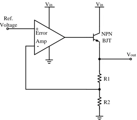
Error Amp Vin Vin Ref. Voltage Vout NPN BJT + -R1 R2
Fig. 2. Linear regulator using NPN BJT as the pass element
There are many configurations for the pass element, such as NPN Darlington, common emitter lateral PNP, NPN emitter follower (NPN BJT), NMOS source follower and common source PMOS transistor [1]. And in these configurations, the most common used are NPN emitter follower, NMOS source follower and common source PMOS transistor. Fig. 2 shows a linear regulator which uses a NPN BJT (Bipolar Junction Transistor) as its pass element. When a BJT is used as the pass element, the output current of error amplifier controls the base of the BJT. As the emitter terminal is connected to output, makes it an emitter follower. And use this emitter follower controlled by error amplifier to regulate the output voltage. The issue of this type of linear regulators is that it will face the stability problem. Because the output impedances of linear regulators those use emitter followers as the pass elements are small. Therefore, the pole created by output node’s RC constant is very large under any loading conditions. The drop-out voltage of NPN BJT is larger than the MOS transistor type, which leads to lower efficiency. And the bipolar junction transistor is more difficult to integrate it into CMOS processes.
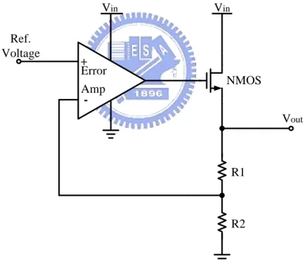
The MOS transistor used as the linear regulator’s pass element will decrease the drop-out voltage and makes the linear regulator a low drop-out linear regulator (LDO). Fig. 3 shows a low drop-out linear regulator using a NMOS pass transistor where source follower architecture is formed. The issue of this type low drop-out linear regulator is that the voltage at gate terminal of the NMOS transistor should be higher than the voltage of source terminal. When the drop-out voltage is small, it means that the voltage between drain terminal and source terminal is small. It makes that the voltage of gate terminal even higher than the voltage of drain terminal. So the supply voltage of error amplifier needs to have an additional boost converter to provide a higher voltage level than Vin.
Error Amp Vin Vin Ref. Voltage Vout + -R1 R2 NMOS
Fig. 3. Low drop-out regulator using NMOS as the pass element
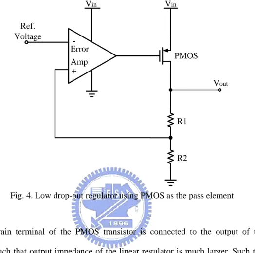
Because of the extra boost converter is extended in the NMOS type low drop-out linear regulator. So the low drop-out linear regulators using PMOS as pass element are widely used. The low drop-out linear regulator using PMOS does not need an additional boost converter such as charge pumps to provide a high voltage level. Fig. 4 shows the architecture of a low
drop-out linear regulator using PMOS as its pass element. Error Amp Vin Vin Ref. Voltage Vout + -R1 R2 PMOS
Fig. 4. Low drop-out regulator using PMOS as the pass element
The drain terminal of the PMOS transistor is connected to the output of the linear regulator, such that output impedance of the linear regulator is much larger. Such that a low frequency pole occurred by the load will pop. So the stability problem will be the issue of this type low drop-out linear regulator.
1.2.2
Switching Regulators
Switching regulators are popular power management devices. It utilize switches to transfer energy and use inductors and capacitors to conserve and deliver energy. The output voltage is controlled by the ON time and OFF time of switches. The output of the switching regulator is an unregulated voltage. The ripple is larger than the linear regulator mentioned
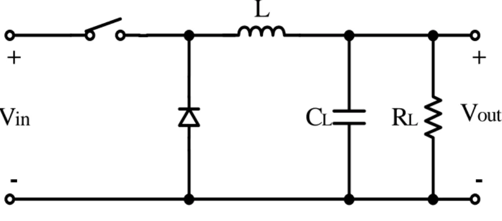
voltage levels. They can variously generate step-up, step-down and combination of step-up and step-down. The step-up switching converters are called boost converters. The step-down switching converters are called buck converters. And the switching converters combine step-up and step-down are called buck-boost converters [2].
+
-+
-V
inC
LR
LV
outL
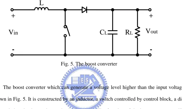
Fig. 5. The boost converter
The boost converter which can generate a voltage level higher than the input voltage is shown in Fig. 5. It is constructed by an inductor, a switch controlled by control block, a diode as a switch, a load capacitor and a load resistor. The function of the boost converter will be mentioned below. First, during the switch is turned ON, the diode is turned of because of the reverse bias, and the supply power Vin will store the power on inductor though the switch as current form. And during the next step when the switch is turned OFF, the energy will be delivered to the output by both input source and the inductor. So the output voltage level is boosted to a higher voltage level than the input voltage level.
+
-+
-V
in
C
LR
LV
out
L
Fig. 6. The buck converter
Fig. 6 shows the architecture of the buck converter. Buck converter can deliver an output voltage lower than the input voltage. Let’s see how it works. First, during switch is turned ON, the diode is reverse biased by the input voltage and being turned OFF. Input voltage source than provide energy to the load through inductor. After that, during switch is turned OFF, the diode will be turned ON and the energy in the inductor which stored in previous state will deliver to the output load capacitor through diode. Then the output voltage is a constant voltage level lower than the input voltage if inductor L and capacitor CL form an low-pass filter.
+
-+
-V
inL
C
LR
LV
outFig. 7. The buck-boost converter
Fig. 7 is the block diagram of a buck-boost converter. We could cascade a boost converter and a buck converter to be a buck-boost converter. A buck-boost converter can
generate an output voltage higher or lower than the input voltage which depends on the input voltage level. If the input voltage is too high, it will generate a lower output voltage. If the input voltage is too low, it will generate a higher output voltage. Such that we can produce a constant output voltage weather the input voltage is higher or lower than the output voltage we want. During the switch is turned ON, input voltage source delivers energy to the inductor and turned of the diode with reverse biasing. And next during the switch is turned OFF, only the energy stored in the inductor transfer to the output node.
1.2.3
Charge Pumps
The basic concept of the charge pump is to generate a voltage level higher than the input voltage level of the chip’s supply voltage. But under specific conditions, charge pump can also be used to produce a voltage lower than the input voltage, even more, produce a negative voltage. The main components in a charge pump are switches, capacitors and a control circuit which provides a two phase control signal.
V
inV
outS
1S
4S
2S
3C
flyC
outR
LV
inV
outS
1S
4S
2S
3C
flyC
outR
LFig. 9 Phase 2 of the basic charge pump
Fig. 8 and Fig.9 show the two phases of a basic charge pump. During phase 1, as Fig. 8 shows, switches S1 and S3 are closed, switches S2 and S4 are opened and the fly capacitor Cfly is charged by the input voltage to the voltage level, Vin. Next, during phase two, as shown in Fig. 9, switches S2 and S4 are close, switches S1 and S3 are opened. The bottom plate of the fly capacitor Cfly is connected to the input voltage Vin, and the fly capacitor already reserved the charge in previous phase. So the top plate of the fly capacitor will be pushed to the potential of twice the input voltage, 2Vin. And there is an output capacitor to transfer this generated high voltage, as the presence of the output capacitor, the output voltage will not be 2Vin and will be an ideal output voltage given by
2 fly out in fly out C V C C = ⋅ + ⋅ (1) V
When the charge pump has a load resistor, RL, connected to the output node, a ripple
voltage will arise. We can make output capacitor as large as possible to minimize the ripple voltage. But if we enlarge the output capacitor, the output voltage will be reduced. So it is a trade off to choose the proper sizes of output capacitor and the fly capacitor.
1.3 Motivation
LCD panels are going more and more popular. The applications of the LCD panels are widely spread in our daily life. From the small LCD panels on palmtop entertainment machine and cell phone to the large LCD panels on LCD TV or outdoor display screen. Therefore the power supply blocks for LCD panels are more and more important. The needs to integrate the power supply block into the LCD driver circuits are rise in great demands. So we want to reduce the size of the power supply block chip and reduce the use of the external components.
The power sources for LCD panels need different voltage scale to charge and discharge the liquid crystal capacitors. Among the DC-DC power converters, inductive switching converters need external components as inductors and charge pumps need external components as capacitor. Compare these two external components inductors and capacitors, inductors occupy more board area than capacitors. And in the applications, LCDs need a negative voltage to discharge the liquid crystal capacitors. Inductive switching converters can not generate a negative voltage. Therefore, with considering the cost and area, we use charge pumps instead of inductive switching converters. The ripple of the charge pump is reduced by an improved double phase cross-coupled charge pump structure.
This thesis implements a selectable multi output DC-DC converter utilize improved dual phase cross-coupled charge pumps. The input voltage is a high voltage 10V. The circuit can supply 4 different output voltages, 10V, 20V, -10V and 0V. The maximum current load is 50mA.
1.4 Thesis Organization
pump, a new negative to positive charge pump and their integration. In chapter 2, the reviews of the previous charge pumps and their control scheme will be given. The conventional charge pumps will be discussed in this chapter. And then in chapter 3, the proposed charge pump circuit and their design analysis is described. The switching technique for output the different output voltage is also presents in chapter 3. In Chapter 4 you can find our sub-circuit design and the simulation results. And the conclusion will be given in chapter 5.
Chapter 2
Review of Charge Pumps
2.1 Introduction
Charge pumps are also called switching capacitor DC-DC converters. Because that charge pumps use the switching of capacitors to converter DC levels. We can obtain a higher, lower or an even negative voltage from a charge pump. Charge pumps are finding grown attention in different systems, especially those incorporating nonvolatile memory, such as EEPROM [3] and flash memories, for the programming of the floating-gate devices [4]. The NOR and DINOR Flash memories, require very high positive and negative voltages to do the operations of programming and erasing. If we have only one single power supply voltage, so we need a charge pump to generate such positive and negative voltages on chip. When it comes to NOR Flash memory, the word-line for erasing is set to about -8V and the word-line for programming is set to 12V, respectively. And charge pumps are widely used in low supply voltage devices to generate a higher voltage level to drive the analog circuits, such as switching regulators. And other applications are dynamic random access memory circuits (DRAM) [6] and low dropout voltage regulators [6].
2.1.1 Charge Redistribution
Charge pump circuits use the switching of capacitors to transfer energy and to boost the voltage level. When charge transfers from one capacitor to another capacitor, there is a charge redistribution process. The process will transfer the energy and redistribute the charge on capacitors.
C
1C
2+
V
1_
+
V
2_
C
1C
2+
V
_
+
V
_
Fig. 10 Charge redistribution
Fig. 10 shows the basic operation of the charge redistribution process. When the switch is opened, the voltage on capacitor C1 is V1 and the voltage on capacitor C2 is V2. The total
charge in the circuit is Q:
1 1 2 2
Q=C V⋅ +C V⋅ (2)
And when it comes to next phase, where the switch is closed. The voltage on both capacitors C1 and C2 are the same. And the total charge Q is equal with the previous phase.
Then the charge will redistribute on two capacitor and we can get the voltage V with:
1 2 Q V C C = + (3)
1 2 1 1 2 1 2 C C V V C C C C = ⋅ + + + ⋅V2 (4)
2.2 Different Charge Pump Circuits
Charge pumps have been proposed for ten years or so. There have been different charge pump types proposed before. In this section, we will describe different types of charge pump. Each one has it own improvement and applications.
2.2.1
Cockcroft-Walton Charge
Pump
This type charge pump can be seen as the prototype of charge pumps. The structure was use by John Douglas Cockcroft and Ernest Thomas Sinton Walton to generate voltage potentials of more than 800,000 volts and help them won the Nobel Prize 1951 in Physics. It uses just switches and capacitor to generate higher voltage. And so it was named Cockcroft-Walton charge pump. The new charge pumps proposed nowadays are based on this principle. VDD VOUT C1 C2 C3 CA CB f f f fb fb fb
Fig. 11 Cockcroft-Walton charge pump circuit
The Cockcroft-Walton charge pump is shown in Fig. 11. Let’s see how it works. When the switches are switched to phase ϕ , capacitor CA is connected to the supply voltage VDD
and charged to voltage, VDD. And during the next phase, the switches are switched to ϕb, the
capacitor CA will be connected parallel with capacitor C2. And the charge redistribution will
operate and if the CA and C2 are in the same size, the voltage o them will be half the supply
voltage, 1
2VDD. And in the next, C2 will be connected to CB and redistribute a voltage of 1
4VDD. The CA will be charged to VDD again. As the procedure goes, after a few cycles, the C1,
C2 and C3 will be charged to the potential VDD and provide a output voltage of 3VDD.
C
3C
2C
4C
1V
inV
outD
1D
2D
3D
4V
1V
2V
3Fig. 12 Cockcroft-Walton charge pump using diode
Fig. 12 shows the circuit of Cockcroft-Walton charge pump using diode to implement. Vin is a square wave swing between VDD to ground. During Vin is at high, V1 will be pulled
high, D1 will be turned off and D2 and D4 turned on. C2 will be charged by input voltage
through D2 to voltage, VDD. During next phase, where input voltage is at ground level, there
will be charge redistribution occurred between C1, C3 and C2. As C1 and C3 is half the size of
C2, the voltage level at V2 and V3 pulled to VDD/2. After a few cycles, the output voltage, Vout,
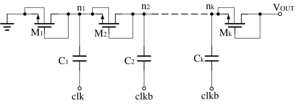
2.2.2 Dickson Charge Pump
The Cockcroft and Walton charge pump has its limitations. To overcome the limitations, a new charge pump structure was proposed by John F. Dickson in1976 [7], as shown in Fig. 13. The charge pump then called as “Dickson Charge Pump” because it was proposed by John F. Dickson. Its operation theorem is similar with Cockcroft and Walton charge pump circuit. The diode chain is coupled to the inputs via capacitors in parallel in the Dickson charge pump instead of in series as Cockcroft and Walton charge pump. It needs a pair of clock input clk and clkb with reversion phases to drive the Dickson charge pump. When clk is high and clkb is at low, the diode between the capacitor connected to the clk and the capacitor connected to the clkb will be turned ON and the capacitor connected to clkb will be charged through the diode. Wen clk is at low and clkb at high, the diode mentioned will be turned OFF and the next diode will be turned ON and transfer the charge to the next stage.
VIN VOUT clk clkb ROUT COUT Cf Cf Cf Cf Cf Cf Cf Cs Cs Cs Cs Cs Cs Cs
Fig. 13 Dickson charge pump with diode and capacitor implementation
The Dickson charge pump with diode implementation is not sufficient for modern IC industry, it needs too much space. To overcome the size problem, a practical implementation of the Dickson charge pump is proposed as shown in Fig. 14. The diodes used before is replaced by diode-connected MOS transistors. It is more suitable for most of the
semiconductor logic process. As shown in Fig. 14, the diodes are replaced by NMOS transistors, therefore the diode forward voltage, VD, is replaced by the NMOS threshold
voltage, Vt, and the threshold voltage Vt is related to the node voltage of each stage.
VDD CLK CLKB C1 C2 C3 Cn Cn+1 VOUT RL COUT V1 V2 V3 Vn Vn+1 C C C C C M0 M1 M2 M3 Mn Mn+1
Fig. 14 Dickson charge pump with MOSFET implementation
The operation of the Dickson charge pump circuit is shown in Fig. 14. It is a typical n-stage Dickson charge pump. The input CLK and CLKB are two out-of-phase clocks with amplitude VCLK. These two clocks will increase the potential voltage in capacitors by
transferring charges in the capacitor chains through diode-connected MOS transistors. The coupling capacitors will be charged and discharged during each half clock cycle. We first define Cs as the stray capacitance at each node. The coupling capacitances are given as C. The voltage difference between the voltages of the nth stage and (n+1)th nodes is given by:
' 1
n n CLK
V
V
+V
V
V
∆ =
−
=
+
t (5) Where the voltage gain can be express as:' CLK CLK C V C Cs ⎛ ⎞ = ⎜⎝ + ⎟⎠V (6)
(
')
OUT DD CLK t t DD CLK S V V N V V V C V N V V C C = + − − ⎡⎛ ⎞ = + ⎢⎜ ⎟ − ⎥− + ⎝ ⎠ ⎣ t⎦ Vt ⎤ (7)The equation above is the ideal output voltage when there is no output load and no output current delivered. When the charge pump is connected to an output load, the load current at a clock frequency f , is given by:
(
)
OUT S L
I
=
f C
+
C V
(8)VL is the voltage drop per stage for supplying the load current. Therefore, the output
voltage will be reduced an N* VL voltage. So the output voltage with load will be rewrite as
follow:
(
OUT)
OUT DD CLK t t S S I C V V N V V C C C C f ⎡⎛ ⎞ ⎤ = + ⎢⎜ ⎟ − − ⎥− + + ⎝ ⎠ ⎣ ⎦ V (9)Above is the operation and equations for an n-stage Dickson charge pump. Next we are going to see the drawbacks of the Dickson charge pump. The major drawback of the Dickson charge pump is the body effect[8][9]. The threshold voltage of a NMOS transistor is given by:
0
2
ln
2
ln
A t t t SB t i iN
N
V
V
V
V
V
n
γ
⎛
⎞
=
+
⎜
⎜
+
−
⎟
⎟
⎝
⎠
An
(10)With the increasing stages of the Dickson charge pump, the threshold voltage will be enlarged. It leads to less voltage gain and poor efficiency. The techniques to overcome the drawback have been proposed. Such as floating well MOS transistor [10], the 4 phase charge pump and the boosted pump clock scheme to fully turn on MOS transistor to reduced the body effect [11][12]; a new clocking scheme to control the charge pump [13] and the CTS scheme. In the CTS scheme, an additional transistor is being added to the circuit, and the gate transistor will be controlled by the next stage voltage. We will discuss these solutions in the next section in detail.
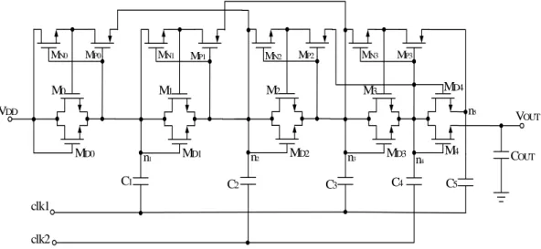
2.2.3 4-Phase Charge Pump
The Dickson chare pump mentioned in previous section is suffering the disadvantage and efficiency loss due to the threshold voltage and body effect. The 4-phase charge pump [14][15] is a solution to cancel the effect of the threshold voltage and body effect.
M0 M1 M2 M3 M4 M5 M6 C1 C2 C3 C4 VDD clk1 clk2 clk1 clk2 clk3 clk4 clk3 Cg1 Cg2 Cg3 Mn VOUT n1 n2 n3 n4 g1 g3 g5
Fig. 15 4-phase n-stage chare pump
The 4-phase n-stage charge pump circuit diagram is shown in Fig. 15. We can see that where the 4-phase charge pump differs from the Dickson charge pump it that the 4-phase charge pump added a MOSFET and a capacitor at each stage. The additional bootstrapping circuits on the gates of NMOS pass transistors are the main contributors to eliminate threshold voltage effect. By added the additional bootstrapping circuits, the gate voltages of NMOS pass transistors are boosted to a higher voltage level than the drain voltage. By doing so, the NMOS pass transistors are fully turned on. Fully turned on NMOS pass transistor allow source and drain terminals to be equalized to the same voltage potential while charge transferring through the pass transistor. The drawback of this design is the extra bootstrapping
circuits needed per pump stage and the extra clocking scheme circuit, it leads to larger chip area. But with the additional circuits, the gain of the 4-phase charge pump can be significant improved. Over the same chip area, the 4-stage charge pump can achieve higher gain and higher charge transfer efficiency.
V Time clk1 clk2 clk3 clk4 Time Time Time
Fig. 16 4-phase chare pump clocking scheme
The operation of the 4-phase charge pump is going to be unfolded. As we can see in the Fig. 15, clk1, clk2, clk3 and clk4 are the non-overlapping clocks. Fig. 16 shows the clocking scheme of these four clocks. In Fig. 15, in the first stage consists of M0 and C1, when clk1 is
low, the diode connected pass transistor M0 is turned on and charges the capacitor C1 to the
voltage level VDD− . Once when the voltage of node n1 is lower than Vt VDD−Vt, the pass transistor M0 is turned on and charge C1 to VDD− . In the next stage, which is consists of Vt
M1, M2, C1, C2 and Cg1. When clk1 is low, clk2 is high and clk3 is low. Node n2 is pulled
high by clk2 through capacitor C2 and turned on pass transistor M2. Capacitor Cg1 will be
charged and push node g1 to a voltage about VDD− . We can see that the gate of pass Vt transistor M1 is not connected direct to the drain as diode connected, it is connected to Cg1.
And during next phase, clk3 changes from low to high and push the gate of M1 to a higher voltage than its drain terminal. Therefore the pass transistor M1 is fully turned on. The
threshold voltage of M1 is canceled when M1 is fully turned on to conduct. The charge will completely pass through M1 and makes nodes n1 and n2 at the same voltage level. And we analysis the n-stage 4-phase charge pump as we did with Dickson charge pump, the output voltage is given by:
(
OUT)
OUT DD clk S S I C V V n V C C C C f ⎡⎛ ⎞ ⎤ = + ⎢⎜ ⎟− ⎥ + + ⎝ ⎠ ⎣ osc ⎦ (11)The threshold voltage Vt is canceled and the efficiency of the charge pump is improved
with the bootstrapping circuit attached.
2.2.4 Static CTS Charge Pump
The charge pump introduced in previous section is a design scheme of canceling threshold voltage Vt effect. In this section we will introduce another design approach of the
threshold voltage Vt cancellation scheme. It is a static charge transfer switches charge pump
[16][17] as shown in Fig. 17. The difference between circuit in Fig. 17 and the 4-phase charge pump in previous section is that it does not need an extra capacitor an extra clocking scheme. Therefore the chip area can be further reduced and at the same time canceling the threshold voltage effect. The gain of the charge pump with charge transfer switches is being raised.
VDD VOUT C1 C2 C3 C4 C5 clk1 clk2 clk1 clk2 clk1 M0 M1 M2 M3 MD0 MD1 MD2 MD3 MD4 n1 n2 n3 n4
Fig. 17 Static CTS charge pump
As we can see in Fig. 17, every stage of the static charge pump consists of two NMOS transistors and a boosting capacitor. At the first stage, MD0 is diode connected as in Dickson
charge pump. M0 is the new circuit added to cancel the threshold voltage of the NMOS. When
clk1 is low and clk2 is high, if capacitor C2 already stored a voltage potential 2VDD in the
previous phase, node n2 will be boosted to a higher voltage as 3VDD (If the clock high voltage
is set to VDD). The node n2 is connected to the gate of pass transistor M0, so the gate of M0 is
connected to a higher voltage than its drain voltage and being fully turned on. Therefore the voltages at its drain and source can be equal while conduct. In the first to the fourth stage in the Fig. 17, the effect of the threshold voltage has been canceled. The voltage gain for each stage is given by:
(
LOAD)
GAIN CLK S S I C V V C C C C f = − + + (12)Compare with the Dickson charge pump, the voltage gain is increased a threshold voltage Vt. But at the last stage, the voltage gain is the same as Dickson charge pump with
threshold voltage Vt. Because the gate of the charge transfer switches is connected to the next
an N-stage static CTS charge pump is given below:
(
LOAD)
GAIN CLK t S S I C V N V C C C C f ⎡ ⎤ = ⎢ − ⎥ + + ⎣ ⎦−V (13)There is a critical drawback in this static CTS charge pump. Although the pass transistors can be fully turned on when conduct, is will also be turned on when it is supposed to be turned off. Because when clk1 is high and clk2 is low, pass transistor M0 is supposed to be
turned off, but node n2 which connected to the gate of M0 is still higher than the drain terminal.
It leads to the reverse leakage current which pass through the pass transistor from node n1 to
VDD.
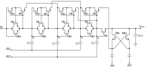
2.2.5 Dynamic CTS Charge Pump
The above-mentioned static CTS charge pump has a critical drawback, the reverse leakage current. In order to fix the defect, a dynamic CTS charge pump [17] [18] is presented in Fig. 18. Each stage in the dynamic CTS charge pump adds an NMOS transistor and a PMOS transistor to control the gate voltage of the charge transfer transistor. In the first stage, an NMOS MN0 transistor and a PMOS MP0 transistor are added to control the gate of the
charge transfer transistor M0. The PMOS MP0 controls the gate of M0 connected to a higher
voltage potential at node n2 from the next stage to fully turn on M0 while transferring the
charge to the next stage. And in the next phase where the charge transfer transistor M0 must be
turned off, the NMOS transistor MN0 will take the responsibility to control the gate of M0. The
gate of M0 is connected to a lower voltage potential at node VDD and insure that M0 is turned
off completely to prevent the reverse leakage current. Although the extra NMOS and PMOS will increase the size of the chip, the gain of the charge pump can be raised and the efficiency
can be improved. VDD C1 M0 MD0 n1 M1 MD1 n2 M2 MD2 C2 n3 M3 MD3 C3 M4 C4 C5 COUT MD4 MN0 MP0 MN1 MP1 MN2 MP2 MN3 MP3 clk1 clk2 VOUT n4 n5
Fig. 18 Dynamic CTS charge pump
Now we consider the final stage of the dynamic CTS charge pump. In Fig. 18, the pass
transistor M3 is turned on by the node n5 when clk1 is high and n5 is at the higher voltage
potential. But during the previous phase, the gate of MD4 is not higher enough to turn on MD4
to charge the capacitor C5 due to the heavy load at the output. The node n5 will not be higher
enough to fully turn on pass transistor M3. To solve this problem, an ameliorated circuit of the
dynamic CTS charge pump is shown in Fig. 19. A bootstrap circuit including two transistors and two capacitors is added to the final stage. This addition circuit is added to ensure that the pass transistor of the final stage can be fully turned on correctly. It uses a pair of cross-coupled NMOS MB1 and MB2 to charge the capacitors, and ensure that the source of the
VDD C1 M0 MD0 n 1 M1 MD1 n 2 M2 MD2 C2 n3 M3 MD3 C3 M4 C4 COUT MN0 MP0 MN1 MP1 MN2 MP2 MN3 MP3 clk1 clk2 VOUT n4 clk1 clk2 MB1 MB2
Fig. 19 Dynamic CTS charge pump with an extra level shifter
There are some improvement researches based on above-mentioned circuits. Such as the charge pump implemented by utilizing PMOS transistors [19]. Design and analysis of the output stage to improve the gain and efficiency of the charge pump [20]. Extra branch added to turn on each other [21].
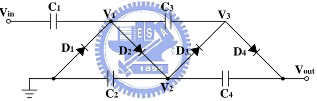
2.2.6 Favrat Charge Pump
The above-mentioned CST charge pumps have improved voltage gain and efficiency. But there is still some deficiencies in the CTS charge pump, such as the gate-oxide reliability for low-voltage operation in CMOS process [21]. Each transistor in the CTS charge pump needs to endure 2VDD voltage. When using a low voltage process and 2VDD exceeds the
process’s maximum voltage, the transistors might breakdown and don’t function as you want. To solve this problem, a structure called cross-coupled charge pump is proposed.
V
DDV
DDV
DDclk
clkb
V
OUTC
OUTM
L1M
L2M
R1M
R2C
1C
2M
B1M
B2M
B3M
B4Fig. 20 Cross-coupled charge pump
The cross-coupled charge pump is shown in Fig. 20. The cross-coupled is proposed in the past for DRAM applications [5]. The cross-coupled charge pump uses two different phases charge pumps. The pass transistors of one charge pump are controlled by the other charge pump in the cross-coupled structure. By doing so, the control circuits can be reduced. In the Fig. 20, while the left side charge pump is charging capacitor C1 through ML1 and MB2,
the right side charge pump is pumping the output to higher voltage through MR2 and MB3. The
ripple of the charge pump can be reduced by applying cross-coupled structure. Because of the two charge pumps is connected together and operate at different phase. And there are two transistors sharing the stresses in each stage, therefore each transistor sustains only the voltage
∆V. Hence, it decreases the risks of break through or breakdown in transistors. The output transistors ML2 and MR2 in the cross-coupled charge pump shown in Fig. 20 run into a
overcome this problem, a more efficiency cross-coupled charge pump is proposed by Pierre Favrat in 1998 as shown in Fig. 21.
VDD VDD VDD clk clkb VOUT COUT ML1 ML2 ML3 MR1 MR3 MR2 C1 C2 CH MB1 MB2 MB3 MB4
Fig. 21 Favrat charge pump
The Favrat charge pump differs from the conventional cross-coupled charge pump at the output stage. An extra capacitor CH and extra transistors ML3 and MR3 are added to the circuit
to solve the problem in cross-coupled charge pump. The capacitor CH will be charged to the
highest voltage 2VDD through ML3 and MR3. The bulk terminals of the PMOS pass transistors
are connected to capacitor CH and push it to the highest voltage 2VDD. By doing so, the turn
on resistors RON of the PMOS pass transistors will be reduced and the gain and efficiency of
the Favrat charge pump can be extended. There are a number of improved charge pumps proposed on the basis of Favarat charge pump. The voltage doubler which is designed to operate at low voltage proposed in [22]. The reduction of the leakage current and conduction
loss in the cross-coupled charge pump and improves the power efficiency [23] [24]. The structure proposed in [25] to reduce the chip area. The body effect eliminating technique utilizing triple-well process [26].
2.3 Negative Charge Pump
The charge pumps mentioned above are all positive charge pumps. The positive charge pumps boost the input voltage to a higher voltage scale which exceeds the source voltage from power supply. If the voltage can be boosted to a higher level, the voltage can be lowered to a lower level too. In modern IC design, the negative voltage which is lower than the ground level is needed. Such as on a DRAM chipset, for the sake of reducing the background leakage current, a negative voltage which is lower than the ground level is utilized to bias the p-substrate instead utilizing the ground voltage level.
2.3.1 Conventional Negative Charge Pump
A conventional negative charge pump is shown in Fig. 22. It is a k-stage 2-phase negative charge pump [27]-[29]. Compare with the positive Dickson charge pump as shown in Fig. 14, the NMOS in the positive Dickson charge pump has been changed to the PMOS in the negative charge pump. The NWELL of the PMOS in the negative charge pump is connected to the most positive voltage per stage. And the source voltage of the first stage in the negative charge pump is connected to ground instead of VDD in the positive charge pump.clk
clkb
M
1n
1M
2n
2n
kM
k+1V
OUTC
1C
2Fig. 22 Conventional k-stage 2-phase negative charge pump
In Fig. 22, the PMOS pass transistors are connected in diode fashion. The operations of the negative charge pump will be given in this paragraph. At the beginning of the pump, the input clock clk is at high as a voltage and the diode connected pass transistor M1 is turned on
and the positive charge from the pump output node n1 of the first stage will be removed and
transfers it to the ground node. And in the next phase, clk is pulled low. Since charge is carried away from node n1 in the previous phase, the voltage level stored in the capacitor C1
will make the output node n1 voltage a negative level. At the same time, the clock clkb is high
and turns on the pass transistor M2 and the positive charge on n2 will be removed and transfer
to n1. And the next clock phase, clkb is pulled low and node n2 is boosted to a lower negative
voltage. The current direction is going through from output node to the input node just opposite of the positive charge pump. The output voltage of the k-stage negative charge pump as shown in Fig. 22 is give by Equation 14.
(
OUT)
OUT clk tp tp S S I C V k V V C C C C ⎡⎛ ⎞ ⎤ V = − ⎢⎜ ⎟ − − ⎥ + + ⎝ ⎠ ⎣ ⎦+ (14)Well Technology
The above-mentioned negative charge pump has the threshold voltage problem [30]. As shown in the Equation 14, the bigger the threshold voltage is, the lower the output voltage can achieve. Therefore if we want to increase the output voltage and the efficiency of the negative charge pump, the threshold voltage of the pass transistors must be reduced. The above-mentioned conventional negative charge pump utilize PMOS as its pass transistor. The bulk terminal of the PMOS transistor in a standard CMOS process must be connected to the highest voltage of the chip. And when it comes to a negative charge pump, the threshold voltage is due to the voltage VSB across source and bulk. The source voltage of the transistor
in a negative charge pump might be a negative voltage lower than the ground level, and the bulk of PMOS transistor is connected to the highest voltage. It makes VSB high and causes the
threshold voltage to be large. The large threshold voltage leads to the decrease of the output voltage. So if we want to increase the voltage gain of the negative charge pump, wee need to decrease the threshold voltage Vt. To decrease the threshold voltage, it can be done by
p-substrate
PWELL
NWELL
NWELL
Deep NWELL
Gate
Fig. 23 Deep NWELL n-type transistor profile
The source to bulk voltage VSB must be minimized to reduce the threshold voltage. The
NWELL of the PMOS transistor needs to be connected to a higher voltage such as Vclk of the
input voltage level. But in a negative charge pump, because of the negative output voltage, an approach to reduce VSB is to switch NWELL potential down to the ground level. By doing so,
the threshold voltage Vt can be reduced due to the reduction of the source to bulk voltage VSB.
Though this approach can reduce VSB, but when the stage increases and the output voltage
goes to a more negative voltage, the VSB is still too large. Therefore if we want to further
reduce VSB, we need the help from the process technology. A deep NWELL NMOS transistor
is introduced in the triple well process technology as shown in Fig. 23. In a normal CMOS process, the NMOS is processed directly on top of p-substrate. If the source of a normal NMOS is boosted to a negative voltage potential, latch-up issues could arise due to the junction forward biasing. A deep NWELL NMOS adds an extra well called deep NWELL as shown in Fig. 23. It will isolate a PWELL from p-substrate. If we connect p-substrate and the extra PWELL together, it is just like a normal NMOS. But with the additional PWELL, the bulk of NMOS can be connected to negative voltage potential. Since the source and bulk of
NMOS can both be connected to negative voltage, source to bulk voltage VSB can be greatly
reduced. Therefore the threshold voltage Vt is reduced.
clk
clkb
M
1M
2M
kV
OUTn
1n
2n
kC
1C
2clkb
C
kFig. 24 k-stage 2-phase negative charge pump with a deep NWELL transistor
With the help of the triple well process technology, a negative charge pump utilizing deep NWELL NMOS transistors is shown in Fig. 24. The bulk and source is butted together to eliminate the body effect. The operation of the negative charge pump in Fig. 24 is the same as above-mentioned conventional negative charge pump.
Chapter 3
The Description and Analysis of the
Proposed Circuit
3.1 Selectable Multi-Output DC-DC
Converters
In some applications, it needs different voltage sources to supply a single node of the chip. Such as the power sources for LCD panels, they need different voltage scale to charge and discharge the liquid crystal capacitors. When we have only one supply voltage scale, we need different DC-DC power converters with different output voltage scales. Among the DC-DC power converters, inductive switching converters need external components as inductors and charge pumps need external components as capacitor. The external component capacitors occupy smaller chip area than the inductors. The amount of external components will increase while we have different DC-DC converters in our chip. Therefore, if we want to reduce the chip area, the external component size must be minimized. The conventional selectable multi-output DC-DC converter utilizes inductive switching converters which occupies larger chip area. The proposed selectable multi-output DC-DC converter utilizes charge pumps as its power converters will reduced the chip area and cost.
3.1.1 Conventional Structure
As mentioned above, the conventional structure of selectable multi-output DC-DC converter uses inductive switching converters as its DC-DC converters. Suppose that the output node needs four voltages, we need four inductive switching converters to supply the different voltage. At least four inductors are needed and they will occupy a large chip area.
Inductive Switching Converter Inductive Switching Converter VDD VDD VDD VDD 2VDD VDD/2 VDD 0 VOUT Control Circuit 1 Control Circuit 2 Control Circuit 3 Control Circuit 4
Fig. 25 Conventional structure of a selectable multi-output converter
As shown in Fig. 25, it is the structure of a selectable multi-output converter. It uses inductive switching converters as its DC-DC power converters. In Fig. 25, there are four
voltages for output switching, VDD, 2VDD, VDD/2 and the ground. The voltage potentials VDD
and ground are directly supplied by the input power supply, the other two voltage potentials 2VDD and VDD/2 need two inductive switching converters to generate. The structure can be
extended if the output needs more different voltage potentials.
3.1.2 Proposed Structure
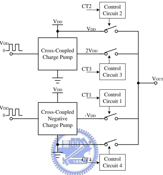
The above-mentioned conventional selectable multi-output DC-DC converter which utilizes inductive switching DC-DC converters demands large chip area. The control circuits, feedback loop circuits and compensation circuits of the inductive switching DC-DC converters also enlarge the size of the conventional structure. The applications that need a negative voltage potential lower than the ground level mentioned before can’t use the conventional structure. Because the inductive switching DC-DC converter can only generate voltages higher or lower than the input voltage, negative voltage lower than the ground is unavailable. Therefore, we propose a new structure of the selectable multi-output DC-DC converter. The proposed structure is shown in Fig. 26. As you can see in Fig. 26, the DC-DC power converters of the proposed selectable multi-output DC-DC converter is replaced by charge pumps. Charge pumps need no feedback and compensation circuits in the applications that do not need accurate output voltage such as LCD panel gate drivers, charging and discharging of the liquid crystal capacitors and flash memories. The replacement of charge pump can reduce the chip area and the cost. And one of the great contribution is that charge pump can generate negative voltage potential which is lower than the ground level.
Cross-Coupled Charge Pump Cross-Coupled Negative Charge Pump VDD VDD VDD VDD 0 0 2VDD -VDD VDD 0 VOUT Control Circuit 2 Control Circuit 3 Control Circuit 1 Control Circuit 4 CT2 CT3 CT1 CT4
Fig. 26 Selectable multi-output DC-DC converter utilize charge pumps
The proposed structure as shown in Fig. 26 has four voltages 2VDD, VDD, -VDD and
ground for selection. The voltages VDD and ground are directly supplied by the input power
source. The voltage 2VDD is generated by an improved cross-coupled charge pump which will
be introduced in the next section. And the negative voltage –VDD is generated by a
cross-coupled negative charge pump which will be discussed in detail in the following sections. As you can see from Fig. 26, there are four switches separately controlled by four control circuits to select the output voltage. There is only one voltage delivered to the output at one time. You can select the voltage arbitrarily as you want to decide which voltage is delivered to the output at the mean time.
3.2 Improved Charge Pump
In this section the cross-coupled charge pump is discussed in detail. The shoot-though current loss may occur in a cross-coupled structure. The shoot-though current will lead to the reduction of voltage gain and efficiency. The shoot-though current here is the current flow from output to input. For a charge pump which boosts the input voltage to a higher level, the current should flow from input supply to output node. Therefore the shoot-though current is a reversion loss which we do not want it to appear. An improve structure of the cross-coupled charge pump will be proposed to reduce the shoot-though current loss. The more the shoot-though current loss can be reduced, the higher gain and efficiency can be achieved.
3.2.1 Shoot-Though Current Loss
In the cross-coupled charge pump such as the Favrat charge pump, there is a loss called shoot-though current loss. It is due to the control of the pass transistors during switching. As shown in Fig. 27, the voltage transition at the node V1 and V2 can not be controlled during
switching. The shoot-though currents will occur on pass transistors ML1, ML2, MR1 and MR2
which are controlled by node V1 and V2 during switching. The currents I1 and I2 are the
shoot-through currents which arise in pass transistors ML1 and MR1. And the currents I3 and I4
are the shoot-through currents which arise in pass transistors ML2 and MR2. Because the
cross-coupled charge pump is a symmetric structure, therefore the shoot-through current is generated each half cycle in similar way.
VDD VDD VDD clk clkb VOUT COUT ML1 ML2 ML3 MR1 MR3 MR2 C1 C2 CH MB1 MB2 MB3 MB4 I1 I2 I3 I4 V1 V2
Fig. 27 Shoot-though current generation mechanism in Favrat charge pump
Fig. 27 shows the shoot-through current generation mechanism. The voltages V1 and V2
produce shoot-through current in four different ways. Voltages V1 and V2 are the control of
the pass transistors ML1, ML2, MR1 and MR2 and they are switched between VDD and 2VDD.
Let’s see the generation of the soot-through current I1, it is due to the leakage from pass
transistor ML1. During the switching where V1 increased from VDD to 2VDD and V2 decreased
from 2VDD to VDD, at the transition in the initial phase of clock signal where
2 1 tn 1 DD
V
− ≥
V
V
and V
>
V
(14)Vtn is the threshold voltage of pass transistors ML1 and MR1. Under this condition, the first
shoot-through current occurs and flow from node 1 through ML1 to the input power supply
VDD. The second shoot-through current is generated in a similar way as the symmetry of the
cross-coupled structure. Shoot-through current I2 flows from node 2 through MR1 to the input
power supply voltage when
1 2 tn 1 DD
AS shown in Fig. 27, the third and fourth shoot-through currents leak from output node the input power supply. This occurs when pass transistor pairs ML1 and ML2, MR1 and MR2 are
simultaneously conducted, respectively.
V
DD2V
DDV
1V
2I
3I
42V
DD-Vtp
V
DD+Vtp
I
1I
2Vtn
Fig. 28 The occurrence of the shoot-though current during switching
As shown in Fig. 28, The duration of the shoot-through currents I1 and I2 are the blue
regions. And the red regions are the duration that shoot-through currents I3 and I4 occur. I3
occurs when ML1 and ML2 are simultaneously conducted. ML2 is turned on when
2
2
DD tp DD2
tpV
≤
V
−
V
and V
>
V
(16)Based on equation (14), the minimum input power supply voltage VDD to turned on transistor
ML1 during the turning on of the transistor ML2 is given by
(
)
max 2
, 2
2
DD tp tp tn tp tn
V
≥
V
V
+
V
=
V
+
V
(17)The red regions where simultaneous conduction occurs in Fig. 28 increases with the input supply voltage VDD. Therefore, the higher the input supply voltage is, the larger the
region of simultaneous conduction is. It will lead to larger power loss and poor power efficiency.
3.2.2 Proposed Charge Pump with
Loss Reduction Technique
From the discussion in previous section, we want to develop an efficient structure of cross-coupled charge pump to reduce the shoot-through current during switching and the reversion loss. The proposed cross-coupled charge pump circuit is shown in Fig. 29.
VDD VDD VDD clk clkb VOUT COUT ML1 ML2 ML3 MR1 MR3 MR2 C1 C2 CH MB1 MB2 MB3 MB4 Level Shifter Level Shifter clk clkb MR4 ML4 R2 R1
Fig. 29 Proposed cross-coupled charge pump with loss reduction technique
As shown in Fig. 29, in the proposed structure, two transistors (ML4, MR4) and two
resistors (R1, R2) are added into the circuit. Transistors ML4 and MR4 are controlled by an extra
level shifter to ensure the proper turning on and off. The principle of operation of the proposed cross-coupled charge pump is going to be unfolded in this paragraph. In the proposed cross-coupled charge pump, ML4 is turned on when ML2 is turned off and MR4 is
turned on when MR2 is turned off. The transistors ML4 and MR4 are used to increase the
additional current path to charge the gate terminals of the power transistors ML2 and MR2 and
makes them turning off much faster. The resistors R1 and R2 are added to slower the transition
speed of the gate if power transistor ML2 and MR2. It makes power transistors to turn on much
slower due to the additional RC delay.
V
DD2V
DDV
1V
22V
DD-Vtp
M
L1ON
M
L2ON
M
R2ON
M
R1ON
Fig. 30 Simultaneous transitions of control voltages in the proposed structure
The simultaneous transitions of the control clocking signal V1 and V2 is shown in Fig. 30. And the control clocking signal V1 and V2 of the proposed cross-coupled charge pump is
the blue line in Fig. 30. The gate of ML2 is connected to V2 through R1. While V2 is changed
form 2VDD to VDD slower, ML2 will be turned on slower. Therefore the ML1 on will not
overlap to the on time of ML2. This creates a break-before-make mechanism which will
prevent the two transistors from simultaneous conduction. The gate of MR2 is connected to V1
through R2. During the switching of V1 from VDD to 2 VDD, because the charging assistant
current created by MR4 will fasten the speed from low to high, power transistor MR2 will be
turned off quickly. It also creates a break-before-make and prevents MR1 and MR2 from
following guidelines. The resistors need to be design large enough to let the slower transition from 2VDD to VDD of V2 can make sure that ML1 is turned on after ML2 is turned off. And the
size of the additional transistors are big enough to let the faster transition from VDD to 2VDD
of V1 can make sure that MR2 is turned off before MR1 is turned on.
3.3 Negative Charge Pumps
In this section, we are going to present the negative charge pumps with different structure. As mentioned above, the negative charge pumps presented later all use NMOS transistors as their pass transistors. Therefore we need the help of triple well process technique. In the next sections, we will introduce negative charge pumps utilizing NMOS transistors. Then the proposed cross-coupled negative charge pump will be presented. The negative charge pump structures for symmetric and asymmetric NMOS will be introduced next. The reversion loss is occurred in cross-coupled structure. The reversion loss reduction technique will be given in the end of this section. The considerations and discussion of multi-stage negative charge pump will also be introduced.
3.3.1 Negative Charge Pump Utilize
NMOS Transistors
As mentioned in the previous section, the negative charge pump which utilizes NMOS as its switches has higher voltage gain and better efficiency. The reason is that the bulk terminal of PMOS must be connected to the highest voltage of the circuit to prevent P-N junction from forward biasing. When it comes to a negative voltage, the positive bulk biasing will leads to very large threshold voltage Vt. And it will reduce the efficiency of the negative charge pump