338 IEEE ELECTRON DEVICE LETTERS, VOL. 17, NO. 7, JULY 1996
Huang-Chung Cheng,
Member, ZEEE,Tzong-Kuei Kang,
Tzun-Kun Ku, Bau-Tong Dai, Member, ZEEE, and Liang-Po ChenAbstract- A novel technique, which uses C12/02 mixed gas in the electron cyclotron resonance (ECR) etching system, has been proposed to remove the antenna charging effect of the
MOS capacitors with 5-nm-thick oxides during polysilicon gate etching. The C12/02 can cause the trenching effect and prevents the gate oxide from the charging damage. Furthermore, the ECR system can provide high polysilicodoxide selectivity so that the Si substrate under gate oxide is not directly bombarded by the ions. Consequently, the E b d degradation of the MOS capacitors disappears as the trenching effect is apparent by using moderate C12/02 mixed gas.
I. INTRODUCTION
N order to avoid the RIE-induced damage, much effort has been put into the development of high-density plasma sources for dry etching at low pressure, e.g., electron cyclotron resonance (ECR) excitation. Although ECR plasma etching technology for submicron fabrication has many advantages, the plasma nonuniformity is often severe in a low-pressure etching system and easily leads to the so-called antenna charging effect in MOS devices. For this charging effect, it indicates that plasma nonuniformity often leads to the positive or negative charges accumulated in isolated antenna regions of the wafer and subsequent gate charging resulting in oxide degradation [1]-[3]. For the MOS capacitors, a new mechanism of the electrical damage by charging during poly-gate etching has been reported [4], [5]. During the poly-gate etching period, the exposed poly-Si provides a low-resistance path across the wafer so that there is surface current and no charging current. However, as the endpoint approaches, the surface current paths across the wafer become too resistive or disrupted, while the conductive paths surrounding the resist pattern are still intact. This results in a brief period where the accumulated charges can tunnel some weak points so that the Fowler-Nordheim cur- rent ( I ~ N ) becomes very significant. Although the mechanism of antenna charging effect during poly-gate etching has been established, the technology reducing the electrical damage induced by plasma charging during poly-gate etching has not been. According to the mechanism mentioned above, the Manuscriot received October 20, 1995: revised February 20. 1995. This
charging effect can be effectively improved by first etching-off a narrow peripheral edge around the gate-pattern.
11. EXPERIMENT
Polysilicon-gate MOS capacitors were fabricated on the (100)-oriented, 15 0-cm, p-type wafers. After the field oxide with 500 nm thickness was grown on silicon wafers, the gate oxide windows were wet-etched with 100 pm x 100 pm area. The thermal gate oxide was grown in N2/02 ambient to have the thickness of about 5.0 nm. After a 400-nm-thick polysilicon layer was deposited, the samples were POC13- doped to have the resistivity of 20 R/cm2. The polysilicon gate was then defined as a rectangular pattern with 100
x
100 pm2 area by wet etching or plasma etching. The MOS capacitors with wet etching are the control samples. The polysilicon was covered with the aluminum. Finally, the backs of these specimens were etched and deposited with the aluminum metal in order to form the ohmic contact. In this work, ANELVA ECR 6001 was used for poly-Si etching. The etching parameters included: SFG flow rate (10-20 sccm), C12 flow rate (90-105 sccrn), 0 2 flow rate (5 sccm), microwave power (250 W), W power (35 W), chamber pressure (2-3 mTorr) and overetch (10, 50, and 100%).111. RESULTS AND DISCUSSION
In our ECR etching system, for the fluorine-containing plasma, the etching profile is undercut severely and the polysil- icon gate becomes progressively more narrow. However, for the chlorine-containing plasma, the poly-gate is outward slightly because the polymer deposition is easy to accumulate in the two sidewalls of the etched polysilicon [6]. In Clz/Oz etching system, the oxygen radicals can remove the polymer deposited on the polysilicon (form C02, CO, H20). Ions ( O i , Cl:) can also remove the polymer via the ion bombardment during the etching process. Therefore, the polysilicon can be etched by the oxygen and assisting-ion. It is also believed that the chlorine radicals are not onlv weaklv bound to the research was supported in part by the Republic of China National Science
Council (R.O.C. NSC), under Contract NSC-85-2215-E-009-035.
H.-C. Cheng, T.-K. Kang, and T.-K. K~ are with the Department of Electronics Engineering and Institute of Electronics, National Chiao Tung University, Hsinchu, Taiwan, R.O.C.
E.-T. Dai and L.-P. Chen are with National Nan0 Device Laboratory, Hsinchu, Taiwan, R.O.C.
Publisher Item Identifier S 0741-3 106(96)053 12-8.
surface but also mobile on the etched sidewall surface [7], [8], Since C1 radicals can move more rapidly along the polysilicon sidewall surface, it results in an attack of the sidewall bottom and leads to the trenching effect after the polymer removal by the oxygen and assisting-ions. Because high polysilicon/oxide selectivity is very important for the gate etching, only the 0741-3106/96$05.00 0 1996 IEEE
CHENG et al.: NOVEL TECHNOLOGY TO REDUCE THE ANTIENNA CHARGING EFFECTS ~ 339 400 nm
c
No Trench
(b) Fig. 1. 95/5 sccm (C12/02) plasma etching.(a) The SEM picture and (b) schematic of the specimen with
range of 95/5-100/5 sccm C12/02 is chosen. Furthermore, the density of the chlorine radicals increases as the Clz/O:! flow rate ratio is raised from 9515 sccm to 100/5 sccm. Meanwhile, the oxygen additives and assisting ions still effectively remove the polymer. Therefore, the probability of the attack of the sidewalls by chlorine radicals is higher with increasing C1 radicals. Consequently, the 95/5 sccm C12/02 cannot provide a remarkable trench on the polysilicon sidewall bottom, but the 100/5 sccm one can. As the endpoint approaches, the high surface current cannot flow toward the gate oxide, leading to charging damage. Hence, better electrical characteristics can be achieved via this technique. The polysilicon sidewall bottom will exhibit the obvious trenching effect as the polysilicon overetch is set at zero. Generally, the practical process adopts the 35% overetch, at which point the trenching effect on Si substrate is very different due to high selectivity (low oxide etching rate), as will be shown. Hence, a 100% overetch is used for considering the practice as well as depicting the trench effect. After the 100% overetch, the SEM pictures and schematics with the recipes of 95/5 and 100/5 sccm C12/02
are shown in Figs. 1 and 2, respectively.
For the distribution of gate oxide breakdown field ( E b d ) , the
Weibull plots of In {- In [l - F ( E ) ] } for the MOS capacitors with C12/02 (95/5 sccm) 10% and 50% overetch and ones with wet etching are shown in Fig. 3. As shown in this figure, for the specimens with plasma etching, the degradation of E b d
distribution for the MOS capacitors is obvious in comparison
Resist
(b) Fig. 2.
100/5 sccm (C12/02) plasma etching.
(a) The SEM picture and (b) schematic of the specimen with
U 5 nm Oxide : Plasma Overetch 10%
- - 0 - - 5 nm Oxide : Plasma Overetch 50%
2
U
-o- - 5 nm Oxide : Wet Etch14 15 16 17 18 19 20 2.1
Breakdown Field (MV/cm) Fig. 3.
with the gate oxide window of 100 x 100pm2 area.
Time-zero dielectric breakdown distribution for the MOS capacitor
to the control ones with wet etching. It is also found that the data for 10% overetching and 50% overetching matches quite well, as shown in Fig. 3. (It implies that the Ebd degradation
340 IEEE ELECTRON DEVICE LETTERS, VOL. 17, NO. 7 , JULY 1996
IV. SUMMARY
2
-2
t
0d
I
The E b d degradation induced by the ECR antenna charging
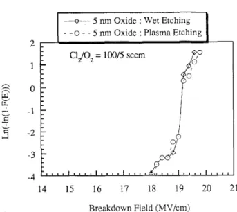
effect on the poly-Si gates can be effectively improved by first etching-off a narrow peripheral edge around the gate-pattern. The technique can be achieved by using 100/5 sccm (Cld02) in the ECR etching system. Furthermore, the good anisotropic profile and high polysilicon/oxide selectivity to avoid direct bombardment of Si substrate under gate oxide by the ions can also be obtained in this etching recipe.
1
ACKNOWLEDGMENT
The authors would like to thank the National Nan0 Device Laboratory of R.O.C. NSC, and SRC of National Chiao Tung r . n ’ n a ‘ ’ I c ’ ’ i I ’ ’ ’ ’ University for technical support.
14 15 16 17 18 19 20 21
Breakdown Field (MV/cm)
Fig. 4. Time-zero dielectric breakdown distribution for the MOS capacitor with the gate oxide window of 100 x 1 0 0 p m 2 area via the trenching technique.
brief period before the poly-gate etching is finished. After the endpoint, the small vertical gate edge is exposed to the plasma, leading to only a small amount of charges accumulated on the poly-gate.) Therefore, the electrical characteristics of the specimens with 10% overetching is similar to the ones with 50% overetching.
The Weibull plots of In {- In [l -
F(E)]}
for the MOScapacitors with C12/02 (100/5 sccm) 50% overetch and ones with wet etching are shown in Fig. 4. In this etching recipe, as endpoint approaches, the periphery of the poly-gate pat- tern will be etched-out at first. Consequently, the antenna charging effect does not occur resulting in better electrical characteristics.
REFERENCES
[l] H. Shin, K. Noguchi, X.-Y. Qian, N. Jha, G. HilIs, and C. Hu, “Spatial distributions of thin oxide charging in reactive ion etcher and MERIE etcher,” IEEE Electron Device Lett., vol. 14, no. 2, pp. 88-90, 1993.
[2] S. Fang and J. McVittie, “Thin-oxide damage from gate charging during ulasma processing,” ZEEE Electron Device Lett., vol. 13, no. 5 , pp.
_ _
i88-290. 1992.131 H. Shin, C.-C. King, T. Horiuchi, and C. Hu, “Thin oxide charging
. .
current during plasma etching of aluminum,” ZEEE Electron Device
Lett., vol. 12, no. 8, pp. 404406, 1991.
[4] S. Fang, S. Murakawa, and J. McVittie, “A new model for thin degradation from wafer charging in plasma etching,” ZEDM Tech. Dig., pp. 61-64, 1992.
[ 5 ] S . Fang and J. McVittie, “Model for oxide damage from gate charging during magnetron etching,” Appl. Phys. Lett., vol. 62, no. 13, pp.
1507-1509, 1993.
[6] S. M. Sze, VLSZ Technology, 2nd ed. New York: McGraw-Hill, 1988,
[7] D. X. Ma, T.-A. Lin, and C.-H Chen, “High selectivity electron resonance etchine of submicron uolysilicon gate structures,” J. Vac.
p. 201.
~~
Technol., pp. 1217-1226, 1992.
181 M. Sato, and Y. Arita, “Etched shape control of single-crystal sili- - . con in reactive ion etching using chlorine,” J. Electrochem. Soc., pp.