行政院國家科學委員會專題研究計畫 成果報告
高階伺服器電源系統數位控制架構之研究
研究成果報告(精簡版)
計 畫 類 別 : 個別型
計 畫 編 號 : NSC 98-2221-E-009-181-
執 行 期 間 : 98 年 08 月 01 日至 99 年 07 月 31 日
執 行 單 位 : 國立交通大學電機與控制工程學系(所)
計 畫 主 持 人 : 鄒應嶼
報 告 附 件 : 出席國際會議研究心得報告及發表論文
處 理 方 式 : 本計畫可公開查詢
中 華 民 國 99 年 10 月 31 日
行政院國家科學委員會補助專題研究計畫
■成果報告
□期中進度報告
高階伺服器電源系統數位控制架構之研究
A Research on Digital Control Architecture for Advanced Server Power
Supply Systems
計畫類別:■個別型計畫 □整合型計畫
計畫編號:NSC 98-2221-E-009-181
執行期間:98 年 8 月 1 日至 99 年 7 月 31 日
計畫主持人:鄒應嶼 教授
共同主持人:
成果報告類型(依經費核定清單規定繳交):■精簡報告 □完整報告
本成果報告包括以下應繳交之附件:
□赴國外出差或研習心得報告一份
□赴大陸地區出差或研習心得報告一份
□出席國際學術會議心得報告及發表之論文各一份
□國際合作研究計畫國外研究報告書一份
處理方式:除產學合作研究計畫、提升產業技術及人才培育研究計畫、列管
計畫及下列情形者外,得立即公開查詢
□涉及專利或其他智慧財產權,□一年□二年後可公開查詢
執行單位:交通大學電機與控制工程系
中 華 民 國 九十九 年 九 月 三 日
行政院國家科學委員會專題研究計畫期末報告
高階伺服器電源系統數位控制架構之研究
A Research on Digital Control Architecture for Advanced Server Power
Supply Systems
計畫編號:NSC 98-2221-E-009-181
執行期限:98 年 8 月 1 日至 99 年 7 月 31 日
主持人:鄒應嶼 博 士 國立交通大學電機工程系 教 授
一、中文摘要
本研究提出一個混合信號的邊界模式功
率因數修正交-直流轉換器,其中包含類比電
流迴路以及數位電壓迴路。本研究同時提出
一種新型的負載適應增益調適以及帶拒濾波
器於數位電壓方法,使系統輸出電壓在不同
穩態負載情況下可達到相同的動態響應,並
提升迴路的頻寬但仍可使輸入電流具備低總
諧波失真以及高功率因數。在類比電流迴路
中,類比電流比較器磁滯比較區間對於輸入
電流總諧波失真的影響進行分析,並選取適
當的值。在數位電壓迴路中,類比數位轉換
器量化效應會使電流命令波形失真,因此適
當的取樣率以及量化元件的位元長度將被決
定。本論文使用電路模擬軟體 PSIM 驗證所
提出控制架構,並與實驗結果相互驗證所提
出之控制架構的可行性、有效性。
關鍵詞:
功率因數修正、相移脈寬調變、數位控
制、互連效應、整合控制
Abstract
This research proposes a mixed-signal solution
for the control of the power factor correction (PFC)
front-end power supplies in applications to
distributed power supply systems (DSP). This
research develops a mixed-signal implementation
technique for critical mode PFC AC-DC converter
with load adaptive gain scheduling. The peak
current mode control is applied and analyzed by
using the analog circuit. This paper analyzes effect
of the hysteresis band effect of the analog current
comparator in current loop. In digital voltage loop,
the proper quantization resolution of ADC is
determined. The digital voltage controller uses a
digital notch filter to achieve fast dynamic response
and a low total-harmonic-distortion (THD) with
high power factor (PF). A load adaptive gain
scheduling applies for maintaining same dynamic
response of the output voltage at different load
conditions change. The proposed mixed-signal PFC
control scheme has been verified by using computer
simulation with experimental results to validate
feasibility.
Keywords:
distributed power supply, power factor
correction, mixed-signal, digital control, adaptive
gain scheduling.
二、緣由與目的
由於科技發展迅速,數位化與網路化是
現代家庭生活的基本需求,基本家電自動化
與資訊設備都需要電源供應系統,提供高品
質的電源與降低電源損耗是未來電源技術發
展的基本前提。
應用於通信設備、伺服器及資料中心之
電源供應系統具備高效率的能量傳送、高供
電品質、低雜訊干擾、高可靠度,以及具有
良好的線擾動及負載擾動穩健性。為了應付
這些嚴苛的需求,通訊設備及伺服器電源系
統 已 朝 向 分 散 式 電 源 系 統 (DPS) 的 方 向 發
展,圖 1 所示為分散式電源供應架構[1]-[3]。
2.5V 3.3V 5V 12V VRMFront-End Power Supply
AC input +48V power bus . . . Serial Interface DC/DC Converter Total Output Power = 125W Efficiency > 90% @ Maximum Load Size: 3.8”× 1.9” × 0.5” Load regulation < 2% Current Limit: 120% Temperature: -40°C - 80°C CPU CPU Intermediate-Stage Power Supply Buck Regulator Memory LDO Inverter Buck-Boost Regulator Utility 85-260V 50-60 Hz
POL Power Supply
PFC IC PWM IC PFC IC PWM IC LCD CCFL PFC IC PWM IC PFC IC PWM IC 圖1 分散式電源架構
數位式伺服器電源控制系統整體方塊圖
如圖 2 所示,包含前級功因修正 AC-DC 轉換
器與後級相移全橋 DC-DC 轉換器。功因修正
AC-DC 轉換器控制架構包含電流迴路,修飾
輸入線電流波形,提高輸入功率因數,電壓
本計劃擬發展整合功率因數修正 AC-DC 與
相移脈寬調變之數位控制架構應用於高階伺
服器電源之數位控制。
Downstream DC-DC Converter load RL vo i~d AC Line DC Bus Downstream DC-DC Converter load RL vo i~d Downstream DC-DC Converter load RL vo i~d PFC Front-End Rectifier PFC Front-End Rectifier PFC Front-End Rectifier 圖2 可並聯之分散式電源系統架構伺服器電源通常採用分散式供電架構,
前級為功率因數修正交流-直流轉換器,修飾
輸入線電流波形以提高輸入功率因數,並轉
換交流電壓至直流電壓且升壓至 400V,後級
一般採用相隔離型相移脈寬調變全橋直流-直流轉換器,將 400V 電壓隔離並降壓至 48V
或 12V 的中間匯流排,透過控制加快輸出響
應及提高效率。一般對於控制器設計都僅針
對各級轉換器設計,串接兩級轉換器後再討
論相互之間的影響[4]。
三、研究方法與成果
Vin D1 D3 D2 D4 va Q1 Q2 vb Q3 Q4 Ll Lm vAB o v PFC AC-DC Converter: Current wave shaping control Dc-link voltage control Load feed-forward controlPSFB DC-DC Converter: Current loop control voltage loop control Load feed-forward control Line feed-forward control
圖3 伺服器電源數位控制的系統方塊圖
圖 3 所示是一個典型的伺服器電源數位
控制的系統方塊圖。主動式 PFC 轉換器必須
藉由高開關頻率控制輸入的電流波形使其與
線電壓同相,達到功率因數為 1.0 的目的,但
此高頻切換也同時產生了額外的高頻電磁干
擾,為了降低其傳導性電磁干擾,在其前端
必須加入適當設計的 EMI 濾波器。此濾波器
與 PFC 轉換器所形成的迴路在某些工作條件
或干擾信號可能會造成系統的不穩定。因
此,濾波器與 PFC 的控制迴路設計均必須一
起考量,確保電源的功率因數、電磁干擾與
穩定性[5]-[8]。
目前純類比實現的功率因數控制晶片雖
然可以達到輸入電流低諧波失真,但類比電
路較易受到溫度的影響並且較難實現複雜的
控制架構;而數位電路實現具有可程式化、
長時間工作的穩定性以及較少的外加元件特
性,可是數位電路受限於類比數位轉換器
(analog-to-digital converter, ADC)和數位類比
轉換器(digital-to-analog converter, DAC)取樣
頻率以及解析度的影響,其準確度較低。
本研究針對如何整合類比電路與數位電
路的優點進行控制架構設計。邊界導通模式
的電流迴路為峰值電流控制,由於邊界導通
模式開關為變頻操作並且在零電流處有高頻
的開關切換,若數位電路實現則需極高頻的
時脈因而造成大量的能量損耗,因此電流迴
路以類比電路實現。電壓迴路頻寬通常不
高,可以用低頻的時脈實現,並且為便於負
載適應增益調變機制的實現,因此電壓迴路
採數位電路實現。
迴路提供輸出直流鏈電壓穩壓,負載前
向控制提高輸出響應速度而不致影響輸入線
電流波形失真。而相移全橋 DC-DC 轉換器控
制架構包含電流迴路,使電流具高頻寬,並
可將系統特性由共軛根解耦為兩個實數根,
可簡化電壓控制器設計,電壓迴路控制輸出
電壓穩壓,負載前向控制提高輸出響應速
度,輸入電壓前授控制可降低兩倍線頻漣波
對輸出影響。
本研究提出一個混合信號控制的邊界模
式功率因數修正交直流轉換器[9]-[12],圖 4
為系統架構方塊圖,其中電流迴路以類比方
式實現,電壓迴路則以數位電路實現。電壓
迴路控制器中,電壓補償器為 PI 控制器,以
消除輸出電壓穩態誤差;數位帶拒濾波器
(notch filter)用以消除輸出電壓兩倍頻對於控
制迴路的影響;由於在不同穩態狀況下,系
統動態響應隨之變動,同樣大小的負載變動
量,會有不同的暫態響應,因此加入負載適
應增益調適使得不同負載狀況下同樣大小的
負載變動量能有相同的暫態響應。
Load Adaptive Gain Adjustment Vout 400V DC GND Vg Cout S A/D H + − Vref MULT ZCD CS × Vcomp INV IL,pkref
Digital Voltage Controller
Analog Current Controller
A/D Ki D/A EMI Filter + -ZOH sense R Current Comparator SR Flip-Flop Digital Notch Filter A/D Digital Voltage Loop Regulator IOF Load Adaptive Gain Adjustment Vout 400V DC GND Vg Cout S A/D H + − Vref MULT ZCD CS × Vcomp INV IL,pkref
Digital Voltage Controller
Analog Current Controller
A/D Ki D/A EMI Filter + -ZOH sense R Current Comparator SR Flip-Flop Digital Notch Filter A/D Digital Voltage Loop Regulator IOF 圖4 具負載增益調適混合信號控制之邊界模式功率 因數修正交-直流轉換器系統方塊圖 ig1 iL,ref iL Ipk ig ig1 iL,ref iL Ipk ig 圖5 電感電流、線電流與線電流基頻成分的關係
類比電流比較器主要用以比較開關電流
回授信號與電感電流命令封包,當開關電流
回授信號頂到封包命令時,則關閉開關。在
類比電流比較器設計上,為了降低雜訊的影
響通常會加入一個磁滯比較區間,不過這個
磁滯比較區間卻會帶給電感電流命令一個直
流值的提升,進而使得輸入線電流在零交越
處失真,因此選擇適當的磁滯比較區間使得
此磁滯比較區間,使線電流滿足諧波規範。
電流比較器磁滯比較區間大小、線電流
波形以及線電流基頻成分波形的關係圖如圖
2 所示;其中磁滯比較區間在電感電流封包中
所造成的直流成分為ΔH
1,線電流波形為 i
g,
而線電流基頻成分為 i
g1。
根據分析可以推得磁滯比較區間與線電
流的關係如圖 6 所示,而輸入線電流的大小
通常可由設計者進行決定,因此可以決定適
當的磁滯比較區間。在本論文中設定於滿載
情況下線電流至少要低於 5%,則由圖 3 可以
得知如要滿足此需求,磁滯比較區間至少需
低於 65 毫伏,本文選取 50 毫伏。
在 PFC 數位電壓迴路的實現設計,整流
後線電壓回授主要用以產生電感電流命令信
號,其直接影響到電流命令的失真量,因此
類比數位轉換器與數位類比轉換器的取樣頻
率與量化效應需加以考慮。
0.020 0.03 0.04 0.05 0.06 0.07 0.08 0.09 0.1 1 2 3 4 5 6 7 8 Hysteresis Band (V) Li ne C u rr ent T H D (% ) Line Voltage: 85 Vrms Line Voltage: 110 Vrms Line Voltage: 165 Vrms Line Voltage: 220 Vrms Line Voltage: 265 Vrms 圖6 電感電流、線電流與線電流基頻成分的關係 1 % 圖7 半弦波電流之頻譜在取樣頻率的設定上,由信號處理中的
取樣定理可知,當預取樣信號的頻譜如範圍
在
ω
n以內,而此時取樣頻率
ω
s如小於兩倍的
ω
n值,此時取樣後之信號會失真。在取樣頻
率上欲使取樣後的整流弦波電流無明顯的失
真,因此先對整流後的弦波信號進行頻譜分
析,並假設頻譜中振幅小於 1%的高階量可以
忽略,由圖 7 可以發現當頻率到 1 kHz 時,
頻譜的振幅大約小於 1%,可知取樣頻率至少
需大於 2 kHz 才能使得取樣後的整流弦波波
型較不失真,本研究選取 5 kHz 的取樣頻率。
Quantizer time Amplitude Original Signal Amplitude time Quantized Signal Quantizer time AmplitudeOriginal Signal time
Amplitude Original Signal Amplitude time Quantized Signal Amplitude time Quantized Signal 圖8 量化對於整流後弦波的影響
量化誤差對於一個整流後弦波波型的影
響如圖 8 所示,當一個整流後弦波經過量化
後,會呈現階梯狀的失真現象。而此量化效
應可以等效為一個量化雜訊加入於控制系統
迴路中。為了決定解析度所造成的量化雜訊
影響,而有關量化誤差的模型,主要有兩種
形式,一種為鋸齒波近似另一為方波近似,
而其最壞的狀況為方波近似法,因此對方波
進行傅立葉轉換,可計算出此方波量化雜訊
模型的最大誤差量。
根據 EN61000-3-2 中 Class C 的規範,可
得知其對於線電流各諧波成分方均根值的限
制隨負載不同而變化,必須小於 3%的線電流
方均根值。最壞的狀況發生於,線電壓有最
小方均根時;如果此時 Ki 為 0.0052,則解晰
度必須小於 0.025,因此在整流線電壓回授的
類比數位轉換器,必須至少是 10 位元。
一般功率因數修正交-直流轉換器的電壓
迴路頻寬通常不高,是為了消除輸出電壓兩
倍頻的漣波對於控制迴路的影響;本文為了
提升電壓迴路的頻寬並且仍能維持線電流為
低諧波失真與高功率修正目的,因此在控制
迴路中加入數位帶拒濾波器以有效的濾除輸
出電壓兩倍頻漣波的影響,其系統方塊圖如
圖 9 所示。當此帶拒濾波器的中心頻率(center
frequency,
ω
0)等於λ時,則該點頻率的信號將
被完全濾除,其中分母的一階係數代表當其
振幅掉至 3 dB 點的頻寬大小。藉由轉移函式
欲求其中心頻率時可令振幅為零,而 3 dB 的
頻寬則令轉移函式的振幅掉至其直流值以下
3 dB 的點,因此可設計出針對特定頻率所需
衰減程度的帶拒濾波器。
加入帶拒濾波器使得不僅改善頻寬且能
維持線電流低諧波失真與高功率因數的特
性。由於在不同穩態負載狀況下,系統的動
態響應也會隨之變動,因此在不同穩態負載
下變動相同大小的負載量其回復時間也不
同;為了使系統於不同穩態負載下變動相同
大小的負載量皆能有同樣的回復時間,本文
提出負載適應增益調變機制。
Vref + Vout -Voltage Compensator C(z) H Control-to-Output GCOD(z) KDAC z-1 KADC Notch Filter N(z) 圖9 加入帶拒濾波器之系統方塊圖負載適應增益調變機制主要利用查表法
並搭配內插法,並且增加輸出電流回授,當
負載變化時,控制器的參數也隨之改變。此
可隨負載波動而調整之適應性數位 PI 控制器
基本上是一個控制參數根據不同操作點所設
計的控制器,主要在於根據不同負載調整期
相位補償頻率,此控制器之參數如表 1 所示。
表1 查找控制參數表 Load (%) 10 30 50 70 90 iout (A) 0.025 0.075 0.125 0.175 0.225 α 1 1.036. 1.072 1.108 1.114 β 1 1.0005 1.001 1.0015 1.002圖 10 與圖 11 分別代表輸出電壓暫態響
應在未加入負載適應增益調適與加入負載適
應增益調適機制;在圖 11 中,還未加入負載
適應增益調變,其由 10 W 變動於 50 W 時回
復時間為 43 ms,而由 60 W 升至 100 W 時回
復時間為 30 ms;當加入負載適應增益調適機
制後,不管是 10 W 變動於 50 W 或是 60 W
變動至 100 W 情況下,系統動態響應回復時
間皆為 30 ms,因此證實加入負載適應增益調
適機制後,確實能有效的改善系統於不同負
載下之動態響應。
1.88 1.9 1.92 1.94 1.96 1.98 2 397 398 399 400 401 Time (sec) Out p u t Vol tag e ( V ) Load from 10 W to 50 W 1.88 1.9 1.92 1.94 1.96 1.98 2 396 397 398 399 400 401 402 Time (sec) O u tp u t V o ltag e ( V ) Load from 60 W to 100 W 43 ms 30 ms 圖10 加入負載適應增益調適輸出電壓暫態響應,負 載分別由10瓦到50瓦以及60瓦到100瓦 1.88 1.9 1.92 1.94 1.96 1.98 2 397 398 399 400 401 Time (sec) O u tp u t Vol tage ( V ) Load form 10 W to 50 W 1.88 1.9 1.92 1.94 1.96 1.98 2 396 397 398 399 400 401 402 Time (sec) Out p ut Vol tag e (V ) Load form 60 W to 100 W 30 ms 30 ms 圖11 加入負載適應增益調適輸出電壓暫態響應,負 載分別由10瓦到50瓦以及60瓦到100瓦四、結論與討論
本研究提出一個混合信號的邊界模式功
率因數修正交-直流轉換器,其中包含類比電
流迴路以及數位電壓迴路。電流比較器磁滯
比較區間的值定為 50 mV;數位電壓迴路控
制中,類比數位轉換器選用 8 位元,取樣頻
率為 5 kHz,而數位類比轉換器則選用 10 位
元;並加入數位帶拒濾波器以提升動態響
應,並維持線電流低諧波失真與高功率因
數;而負載適應增益調適機制,用於改善不
同穩態情況下的,等量負載變化,使其動態
響應相同,經由模擬與實驗驗證本研究提出
方法之可行性。
五、參考文獻
[1] W.A. Tabisz, M.M. Jovanovic, and F.C. Lee, “Present and future of distributed power systems,” Proc. IEEE
APEC, 1992.
[2] F. C. Lee, P. Barbosa, Peng Xu, Jindong Zhang, Bo Yang, and F. Canales, “Topologies and design considerations for distributed power system applications,” Proceedings
of the IEEE, vol. 89, no. 6, pp.939-950, Jun 2001.
[3] Fred C. Lee, Ming Xu, Shuo Wang and Bing Lu, “Design challenges for distributed power systems,” IEEE IPEMC
Conf. Rec., 2006.
[4] Jian Sun, “Small-signal methods for ac distributed power systems – a review,” IEEE Transactions on Power
Electronics, pp. 2545-2554, vol. 24, no. 11, Nov. 2009.
[5] G. Spiazzi and J. A. Pomilio, “Interaction between EMI filter and power factor preregulators with average current control: analysis and design considerations,” IEEE
Transactions on Industrial Electronics, vol. 46, no. 3, pp.
577-584, Jun 1999.
[6] M. Orabi and T. Ninomiya, “Nonlinear dynamics of power-factor-correction converter,” IEEE Trans. on
Industrial Electronics, vol. 50, no. 6, pp. 578-584, Dec.
2003.
[7] Jian Sun, “Input impedance analysis of single-phase PFC converters,” IEEE Transactions on Power Electronics, vol. 20, no. 2, pp. 308- 314, March 2005.
[8] Min Chen and Jian Sun, “Low-frequency input impedance modeling of boost single-phase PFC converters,” IEEE Transactions on Power Electronics, vol. 22, no. 4, pp.1402-1409, July 2007.
[9] Ming-Hau Chan, Yu-Tzung Lin, and Ying-Yu Tzou, “Load adaptive control for mixed-signal PFC control IC,”
IEEE PEDS Conf. Rec., Taipei, Taiwan, Nov. 2-5, 2009.
[10] Ming-Hau Chan, Yu-Tzung Lin, and Ying-Yu Tzou, “Development of a mixed-signal PFC control IC with fast dynamic response,” IEEE IPEMC Conf. Rec., Wuhan, China, May 17-20, 2009.
[11] Chia-Han Hung, and Ying-Yu Tzou, “MathCAD design of critical conduction mode PFC converters,” IEEE
IPEMC Conf. Rec., Wuhan, China, May 17-20, 2009.
[12] Yu-Tzung Lin, and Ying-Yu Tzou, “Digital control of boost PFC AC-DC converter with low THD and fast dynamic response,” IEEE IPEMC Conf. Rec., Wuhan, China, May 17-20, 2009.
可供推廣之研發成果資料表
■ 可申請專利 ■ 可技術移轉
日期:99 年 9 月 23 日
國科會補助計畫
計畫名稱:高階伺服器電源系統數位控制架構之研究
計畫主持人:鄒應嶼
計畫編號:NSC 98-2221-E-009-181
學門領域:電力
技術/創作名稱
混合信號功率因數修正控制技術
發明人/創作人
鄒應嶼
中文:
本技術『混合信號 PFC 控制技術』針對單相之交直流電源轉換系統
發展結合數位類比混合訊號電路實現的 PFC IC 核心技術,可應用於
升壓式交直流轉換電路功因校正控制晶片之設計,採用混合信號控制
架構,主要包含數位 PWM 產生電路、類比電流控制、與數位相位補
償控制電路。
技術說明
英文:
The developed mixed-signal power factor correction technique can be
applied to single-phase ac-dc converter with unit power factor correction.
The developed technique can be used for boost ac-dc converter for power
factor correction and voltage regulation. The developed technique can be
used to realize cost effective high performance PFC control IC.
可利用之產業
及
可開發之產品
開關式電源供應器、電源設備之數位控制
不斷電系統、功率因數改善設備
電源管理 IC、照明 IC、數位電源 IC、PFC IC、數位 PWM IC
技術特點
混合信號 PFC 控制技術
數位式脈寬調變產生電路、類比電流控制
可應用於非隔離式升壓型交直流 PFC 轉換電路
可應用於 PFC IC 之實現
可應用於電源管理 IC
推廣及運用的價值
混合信號 PFC 控制技術可廣泛應用於各類需要連接市電之電源
設備,本技術提供混合信號 PFC 控制晶片設計的系統架構設計與實
現方法,並以 DSP 與類比電路完成系統整合驗證,可進一步推廣於
各類與市電連結電源系統之應用,或提供 PFC IC 設計之 IP。
※ 1.每項研發成果請填寫一式二份,一份隨成果報告送繳本會,一份送 貴單位研發
成果推廣單位(如技術移轉中心)。
※ 2.本項研發成果若尚未申請專利,請勿揭露可申請專利之主要內容。
※ 3.本表若不敷使用,請自行影印使用。
出席國際學術會議心得報告
計畫編號 98-2221-E-009-181
計畫名稱
高階伺服器電源系統數位控制架構之研究
出國人員姓名
服務機關及職稱
鄒應嶼 教授/國立交通大學電機工程學系
會議時間地點 98 年 9 月 19 日至 9 月 24 日/美國加州舊金山聖荷西市(San Jose, CA)
會議名稱
2009 IEEE Energy Conversion Congress and Expo
2009 年國際能源轉換論暨展覽研討會
發表論文題目
Chia-Hao Wu and Ying-Yu Tzou, “Digital control strategy for efficiency optimization of a BLDC motor driver with VOPFC,” IEEE ECCE Conf. Rec., San Jose, CA USA, Sept. 21-25, 2009.
一、參加會議經過
本人 2009 年 9 月 19 日前往美國舊金山參加 ECCE2009 學術研討會,此研討會是由
國際電機電子工程學會(IEEE)之電力電子學會(PES)與工業應用學會(IAS)所主辦的首屆
IEEE Energy Conversion Congress and Expo,此研討會係結合了 PESC Conference 及 IAS
Annual Meeting 兩大年度重要學術研討會,主要針對『能源』為主題,其領域跨及的技
術層面涵蓋了電力電子、電池儲能、綠色能源、電源 IC 等相關領域。此次研討會於今年
9 月 19 日至 24 日在美國加州聖荷西市(San Jose, CA) 的 DoubleTree Hotel 舉行,有將近
900 位來自 40 幾個國家的與會者,此次邀稿大會收到超過 1200 篇的投稿論文,挑選了
近 600 篇論文。而其兩天的展覽也吸引了近 30 家相關領域的廠商參與展出。
本研討會是電力電子領域最重要的國際學術研討會之一,較著重於學術理論發展,
是新理論與新方法論文發表的重要學術研討會。此次議程包括:直流-直流轉換器、直流
-交流轉換器、馬達驅動器、數位控制技術、電池儲能、綠色能源、電源 IC、功率模組整
合封裝技術、高功率直流轉換器、電磁干擾等等。此次與會除了發表論文外,亦與國際
友人聯絡友誼、交換意見,瞭解這些領域之研究動向與未來發展之趨勢。
二、與會心得
本次研討會著重於綠色能源的發展,特別是太陽光發電、馬達節能技術受到重視,
也有專屬的議程討論。整合類比電路設計與電力電子的應用發展,近年來逐漸受到重視,
小型電源控制與轉換 IC,如充電 IC、電源管理 IC、小型馬達驅動 IC 等等,都具有廣大
的市場發展潛力。交通大學電力電子實驗室本次發表之論文研究著重於數位式電源轉換
與馬達控制 IC 技術之研究與發展,政府目前積極推動綠色能源計畫,鼓勵以電力電子與
綠色能源為導向的系統整合,國內電力電子領域設計人才濟濟,或可結合綠色能源、太
陽光電、風力發電、電源設計、馬達驅動、IC 設計人才,從資訊家電的綠色能源技術領
域著手系統整合的研究。
Digital Control Strategy for Efficiency Optimization of a BLDC Motor Driver
with VOPFC
Chia-Hao Wu
Power Electronic Systems and Chips Lab. Department of Electrical Engineering National Chiao-Tung Univ., Hsinchu, Taiwan
Ying-Yu Tzou
Member, IEEE
Power Electronic Systems and Chips Lab. Department of Electrical Engineering National Chiao-Tung Univ., Hsinchu, Taiwan
Abstract--This paper proposes a dual-mode control strategy for BLDC motor drivers with power factor correction used in high-efficiency compressor applications. The motor driver consists of a front-stage variable output voltage PFC (VOPFC) converter and a rear-stage 3-phase PWM inverter. The VOPFC converter is a cascaded buck-boost converter with two power switches to regulate the input line current with low total harmonic distortion (THD) and at the same time to maintain an adjustable dc-link voltage which can be either higher or lower than the peak of the rectified line voltage. The output inverter stage can be operated in pulse amplitude modulation (PAM) mode or PWM mode with reduced switching frequency for efficiency optimization of the compressor motor driver to maintain a constant V/Hz ratio with specified current ripples. The proposed control scheme has been verified with a DSP-controlled VOPFC PWM/PAM motor driver and an efficiency improvement of 3% has been achieved.
Index Terms--variable output power factor correction (VOPFC), brushless dc motor, compressor driver, dual-mode control, efficiency optimization.
I. INTRODUCTION
BLDC motors have been widely used in various applications, and they have a better efficiency and produce more power for the same size compared to induction motors. For the rotated speed of the motors, the bus voltage of the inverter needs high enough to overcome the back-EMF that is proportional to the speed. The traditional motor drivers are designed as fixed-voltage-control, so the switching frequency of pulse width modulation (PWM) is up 16 kHz to rotate motors for lower current ripples. However the high switching frequency is always along with the large switching losses [1]. Besides, when the motor rotates in slow speed, the duty cycle of PWM module in inverter must be low consequently and the extreme duty cycle may have a greater distortion in the voltage control for the dead time control.
Moreover, it is well know that power supplies connected to AC without power factor correction will introduce high low-order harmonic currents and result poor power quality. Such harmonic currents cause several problems including voltage distortion, heating, radiated and conducted noises and can reduce the capability of the line to provide energy. Recently the demands for high power factor and low harmonic distortion in the current drawn from the utility have been increasing [2]-[3]. As a result, in order to meet the
requirements of high power factor and high efficiency in modern motor driver, the control strategy for high power factor correction and efficiency optimization with the integration of VOPFC and inverter has been developed [4-6].
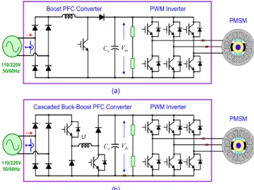
Boost converter is usually employed for the single-phase PFC applications, as shown in Fig. 1(a). But its fixed dc-link voltage will result higher switching losses at light load under low speed operation of the compressor driver. In order to improve the compressor driver at low-speed operation region, a lower dc-link voltage with minimum switching frequency is preferred. The VOPFC converter is a buck converter cascaded with a boost converter shared with a common inductor, and the schematic of the VOPFC inverter driver is shown in Fig. 1(b).
The VOPFC converter provides an adjustable output voltage with a cost of one additional MOSFET and a switching diode. This paper proposes an integrated control strategy of the VOPFC inverter driver for dc-link voltage regulation, line current regulation, and efficiency optimization. The design and implementation of the VOPFC controller are presented and their benefits and limitations are analyzed. Co 110/220V 50/60Hz dc V PWM Inverter PMSM Boost PFC Converter Co 110/220V 50/60Hz dc V PWM Inverter PMSM Cascaded Buck-Boost PFC Converter
Lf
(b) (a)
Fig. 1. Two PFC AC/DC converter topologies for compressor PMSM drivers (a) boost converter (b) cascade buck-boost converter.
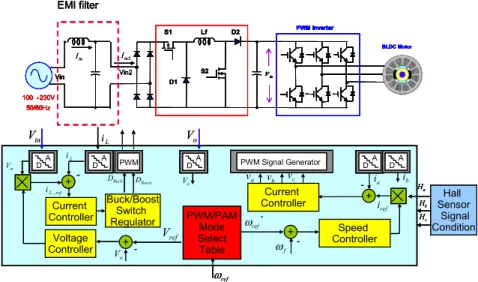
S1 D1 S2 D2 Lf dc V PWM Inverter BLDC Motor dc V PWM Inverter Vin 100 -230V 50/60Hz EMI filter Vin 100 -230V 50/60Hz Vin2 in I Iin2 A DA D PWM DDAA PWM Signal Generator DDAA DDAA Current
Controller SensorHall Signal Condition a H b H c H a i ib a v vb vc + ref i Speed Controller + * ref ω f ω Buck D DBoost Current Controller Buck/Boost Switch Regulator -+ -Voltage Controller in V A DA D ref L i , L i ref V PWM/PAM Mode Select Table + -o V o V in V L i ref ω o V S1 D1 S2 D2 Lf dc V PWM Inverter BLDC Motor dc V PWM Inverter Vin 100 -230V 50/60Hz EMI filter Vin 100 -230V 50/60Hz Vin2 in I Iin2 S1 D1 S2 D2 Lf dc V PWM Inverter BLDC Motor dc V PWM Inverter Vin 100 -230V 50/60Hz EMI filter Vin 100 -230V 50/60Hz Vin2 S1 D1 S2 D2 Lf dc Vdc V PWM Inverter BLDC Motor dc Vdc V PWM Inverter Vin 100 -230V 50/60Hz Vin 100 -230V 50/60Hz EMI filter Vin 100 -230V 50/60Hz Vin2 in I Iin2 A DA DA DA
D PWMPWM DDDDAAAA PWM Signal GeneratorPWM Signal Generator DDDDDDAAAAAA DDDDDDAAAAAA
Current
Controller SensorHall Signal Condition a H b H c H Hall Sensor Signal Condition a H b H c H a i ib a v vb vc + ref i Speed Controller + * ref ω f ω Buck D DBoost Current Controller Buck/Boost Switch Regulator -+ -+ -Voltage Controller in V A DA DA DA D ref L i , L i ref V PWM/PAM Mode Select Table + -o V o V in V L i ref ω o V
Fig. 2. Circuits and control system diagram in the integration of VOPFC and inverter.
II. SYSTEM ARCHITECTURE
This paper proposes the design of VOPFC converter applied to household compress drivers. We selected the circuit of cascaded buck-boost to realize the VOPFC, because the lower cost in the cascaded buck-boost topology lower than in the buck-boost one for reduced size inductor and capacitors can be used [7]. The circuit architecture and system control diagram are as shown in Fig. 2. We cascade the VOPFC converter and an inverter to form a two-stage BLDC motor driver.
As shown in Fig. 3, when input voltage is higher than output voltage, the VOPFC converter is operating in buck mode via buck-switch (S1) to generate the output voltage. On the contrary, when input voltage is lower than output voltage, the system is operating in boost mode via boost-switch (S2) to generate the output voltage.
in
V
Vo 1 S 2 SBuck Boost Buck Boost
t
t
t
inV
Vo 1 S 2 SBuck Boost Buck Boost
t
t
t
Fig. 3. Duty cycle and status of switch S1 and S2.
With the feedback of the motor’s speed and phase current, BLDC motor can be controlled in steady speed and maintain
constant torque. When the compressors work at a relatively low speed, the back-EMF of motor is low. With the VOPFC converter, the bus voltage can be decreased, so the inverter avoids the high switching frequency consuming redundant switching loss to improve the efficiency of the compressor motor. Otherwise, in order to speed up the response of acceleration, the bus voltage increases to meet the back-EMF that is proportional to speed and the inverter is operated in PWM mode.
The inverter controller consists of an inner current loop controller and an outer speed loop controller. The current loop controller regulates motor phase currents with specified current ripples and generates PWM signals according to the Hall-sensor feedback. The speed controller generates a torque current command according to an estimated speed feedback from the measured Hall-sensor feedback. When the motor is running in constant speed mode, the inverter controller can be operated in PAM mode to minimize switching losses or PWM mode to minimize torque ripples with specified current profile.
III. VOPFC CONTROL STRATEGY AND CONTROLLER DESIGN
Fig. 4 is the control block diagram of the cascaded buck-boost converter. The system controller is designed to be multi-loop and it includes the current controller and voltage controller. In order to achieve PFC, the input voltage and the input current should be maintained in-phase. The system uses input voltage as the reference to control inductor current. In the cascade buck-boost circuit, its operation is changing adaptively between buck and boost mode. In order to speed up the response of current loop, a feed-forward compensation controller is employed. It linearizes the transfer function of the current loop in VOPFC converter and simplifies the design of current controller.
A DA DA DA D PWMPWM DDDD AAAA Buck DBuck DBoost D DBoost Current Controller Buck/Boost Switch Regulator + -Voltage Controller in V A DA DA DA D L i Vo ref V -o V o V in V iL ref L iL, ref i , + o V in V o V in V Feed-forward Controller L R L C L D1 D2 S1 S2 ACin
Fig. 4. The cascade buck-boost converter with control block diagram.
A. Small signal analysis and controller design
Due to the need of operating between buck mode and boost mode with the input voltage being a semi-sine wave, a non-static voltage source, the controller design must be considered in different operating points. The current control block diagram is two stages in the system. First stage is a PI controller and second stage is the feed-forward compensation controller.
Before the designing PI controller, the transfer functions of buck and boost modes should be obtained firstly by the state-space averaging method. In boost mode, the transfer function of the converter can be expressed as
[ ]
) ( ) ( ) 1 ( ) ( ) ( ) 1 ( ) ( ) 1 ( ) ( 1 0 1 ) ( ~( ) ~ ) ( 1 1 , s C sI s L D V C I L V s s s C D s L D s C R s s d s i s T L L o L o L L L L Boost p Δ × − Δ × − = ⎥ ⎥ ⎥ ⎦ ⎤ ⎢ ⎢ ⎢ ⎣ ⎡ − × ⎥ ⎥ ⎥ ⎥ ⎥ ⎦ ⎤ ⎢ ⎢ ⎢ ⎢ ⎢ ⎣ ⎡ Δ Δ − Δ − Δ + × = = . (1)By the same method, the transfer function for buck mode can be expressed as
[ ]
L C V s L V C R s C L s s d s i s T L in in L L L L Buck p × Δ = ⎥ ⎥ ⎦ ⎤ ⎢ ⎢ ⎣ ⎡ × ⎥ ⎥ ⎥ ⎥ ⎦ ⎤ ⎢ ⎢ ⎢ ⎢ ⎣ ⎡ + − × = = − ) ( 1 0 1 1 1 0 1 ) ( ~( ) ~ ) ( 2 1 , , (2)where
Δ
1(
s
)
and Δ2(s)areL L L LC D C R s s s 2 2 1 ) 1 ( ) ( = + + − Δ (3) L L LC LC R s s s) 1 ( 2 2 = + + Δ . (4)
The above equations show that the transfer functions of the buck and boost converters are both second-order systems.
The transfer function of boost has a zero but the one of buck doesn’t. After calculating the transfer functions of boost and buck, the bandwidths of current control loop under different operating points are distinctly discussed. Analyzing the small signal models of buck and boost circuit under variable input voltage, the minimal bandwidth and worst response appeared at the border of buck and boost. The bode plots of the buck and boost are shown in Fig. 5. The SISO tool in the MATLAB was used to synthesize the compensation zero of PI controller for the current loop. The goal for design of current controller would increase the bandwidth of current loop to improve response speed.
10 20 30 40 50 60 70 M a gn it ud e ( d B) 100 101 102 103 104 -135 -90 -45 0 45 90 P has e ( deg ) Bode Diagram Frequency (rad/sec) Boost Buck Buck Boost 10 20 30 40 50 60 70 M a gn it ud e ( d B) 100 101 102 103 104 -135 -90 -45 0 45 90 P has e ( deg ) Bode Diagram Frequency (rad/sec) Boost Buck Buck Boost
Fig. 5. The bode plots of the transfer functions of buck and boost when input voltage is 100V.
After designing the first stage current controller, the feed-forward compensation controllers in second stage were designed independently for buck mode and boost mode.
B. Feed-forward Compensation Controller
In order to let the system have the quicker speed of response, the paper proposes the design of the multi-loop controller for the buck-boost circuit as shown in Fig. 6. The minor loop is current control and the major loop is voltage control. In order to linearize and improve the current response, the feed-forward compensator controller is designed as shown in Fig. 7. With the current compensator, the current response has the lower steady state error and the PI compensator design can be simple, even if the system is operated alternately in buck or boost modes.
Vo_f V_err + -Sampling frequency: 2k Hz Vkp Vki z-1 + + + + Q6 Q10 Vcom Sampling frequency:20kHz Ikp Iki I_f Iref I_err I_err3 z-1 Vd + -+ + BBuck/Boost Switch Regulator + + Q6 Q10 Vin Vco V_err3 I_mag Q3 Q6 DBoost DBuck Feed-forward controller Vin Vo_f
Sampling Frequency:20kHz Ikp Iki I_err I_err3 z-1 + -+ + + + Q6 Q10 Q6 in V IL mag I Iref out V
Current Feed-forward Controller
Pulse Width Modulator x y y x d−1 + _ in V d V out V d x y y x + + in V d V kd kd − + + -0~Kd -Kd~0 DBoost DBuck
Pulse Width Modulator
Current Loop Compensator Kc(s)
L I
Δ
Fig. 7. System block diagrams of the feed-forward compensator controller and current controller.
After designing the first stage current controller, the
second-stage was continuously designed separately for buck
and the boost circuit characteristics.
When system is operated in boost mode, the current
incremental ΔiL in the input inductor during a PWM
switching period Ts with duty ratio of d can be expressed as
[
V d V]
TL I s out in L= −(1− ) Δ . (5)This is the desired voltage that we need to apply to the
inductor, let’s denote as Vd. It can be expressed as
out in
d V dV
V = −(1− ) , (6)
where Vd is the output of the PI controller KC(s) and it is the
command of the voltage that we want to apply to the inductor to result a increment current to reduce the current error as shown in Fig. 7. d V V V out d in− =1− (7)
The PI current compensation controller KC(s) can improve the
steady state error.
The consideration in buck mode is similar with boost
mode. Vd is the output of the PI current loop controller KC(s),
which is the voltage we want to apply to the inductor to result
a current increment of Δ to reduce the current error. IL
d V V V in out d + = (8)
With the employment of the feed-forward compensator for the current loop regulation, the current response can be improved significantly to achieve low current harmonic distortion.
C. Inductor current command compensation
When the system is operated in boost mode, buck-switch
(S1) is constantly conducted and input current is equal to
inductor current. The ripple of inductor current can be reduced by selecting the proper inductance, hence decreasing the THD of the input current. However, during the buck
mode, the current through S1 is the input current, ant it is
intermitted due to the switching of power switch. As a result, an EMI filter is required to decrease THD to improve PF.
As known form the above, if the duty cycle of switch S1 is
DBuck, the input current can be calculated by
L Buck
in
D
I
I
=
×
(9)where Iin is the input current and IL is the inductor current. If
the inductor current command maintains the waveform as sine-wave, the input current will be non-sine-wave. Consequently, a compensation of inductor command is required in buck mode.
Because the input voltage V is converted into a stable in
DC voltage from a rectified semi-sine-wave via converter, according to the characteristic of buck converter, during continuous current mode (CCM), operation status of the system are as the following.
)
sin( t
V
V
in=
dω
(10) in o Buck V V D = (11) L d o L Buck in V t I V I D I = × = × ) sin(ω
, (12)where Vois input voltage and DBuck is the duty of S1.
From (12), if inductor current I is proportional to input L
voltage, the input current will be the constant value and the waveform will be distorted. As a result, a current compensation is implemented to eliminate this problem. In
according to (12), inductor current command IL_ref in buck
mode is corrected as the following:
Buck d
ref
L K t D
I , = sin(
ω
)× 1 (13)From (12) and (13), it can be suggested that input current becomes sine-wave after compensation, as shown in Fig. 8.
IV. INTEGRATION SYSTEM DESIGN
A. Inductor ripple current analysis
During operation of a motor, the current is proportional to output torque and back EMF is proportional to the rotation
speed. As shown in Fig. 9, ripple current Ia isΔ , during this i
operation condition, Ia pass through switches S1 and S6 or S2
and S6. Because the current flow through two switches
simultaneously, the switching conduction loss is analyzed as follows: s s dc i L D T V V × × − = Δ ( ε) (14)
2 ) ( 3 1 1 avg i avg RMS I I I = + Δ (15) 2 _ 2 _Loss RMS ds on
2
RMS CI
R
I
P
=
×
×
∝
(16)Above equation suggests that switch conduction loss is related to ripple current in identical switching component. Switch conduction loss can be controller if inductor ripple current is controlled. 0.0 -2.00 2.00 IinVin IVac/78in 0.0 -2.00 2.00 IinVin IVac/78in (a) 0.0 -1.00 1.00 2.00 3.00 4.00 5.00 I(La)
IL
I_ref Buck Buck 0.0 -1.00 1.00 2.00 3.00 4.00 5.00 I(La)IL
I_ref Buck Buck (b)Fig. 8. (a) Input current and input voltage and (b) inductor current command and inductor current in VOPFC converter.
dc
v
1 s s3 s5 2 s s4 s6 A B C c a b b e a e n c e s L s R s L s R s L s R (a) tt a i avg i i avg i + Δ 0 i avg i −Δ avg i − i avg i +Δ − i avg i −Δ − a i avg i i avg i + Δ 0 i avg i −Δ avg i − i avg i +Δ − i avg i −Δ − (b)Fig. 9. (a) Schematic of the inverter and the BLDC motor. (b) Illustrated waveform of phase current under closed-loop PWM control.
Assuming speed and load torque of motor are constant,
and back-EMF V is proportional to motor speed. The ε
motor controller is operated under different bus voltage Vd1
and Vd2, the current ripples can be calculated from (14), and
the relationship of Δi1and Δi2 is expressed as
2 2 2 1 1 1 s dc s dc s dc s dc T V V L V V T V V L V V × × − = × × − ε ε ε ε . (17) 1 2 2 1 1 2 2 1 1 1 dc dc dc dc dc dc s s V V V V V V V V V V T T ε ε ε ε − − = × − − = , (18)
where Ts1 and Ts2 are the periods of stitching.
According to the above equations, as motor drive is operated under a lower bus voltage, the switching frequency decreases accordingly to maintain the same level of inductor current ripple with the same conduction losses of power switches, and switching loss decreases significantly to improve the efficiency.
Fig. 9(a) and Fig. 10 show that high side switch and low side one switch alternately under a fixed switching frequency. During the transition of switching of power switches, the voltage waveforms and the current one overlap and result the
switching losses in power switches [8]. The losses Ps_LOSS
after one complete cycle are calculated.
off d dc on d dc off on t i V t i V P P 2 _ _ 1 2 2 × + × = + (19) Assuming
t
d_on≈
t
d_off=
t
d s dc s d dc avg L s d dc s off s on s Loss S f V f t V i f t V i i T P P P × ∝ × × × = × × × + = + = , 2 1 _ _ _ 2 ) ( , (20)where i and 1 i2 are the maximum and minimum of the
inductor current, td is switching overlap, and fsis the
switching frequency.
From (18) and (20), the ratio of switching losses in different bus voltages can be expressed as
ε ε ε ε V V V V V V V V V V T T V V f V f V P P dc dc dc dc dc dc s s dc dc s dc s dc s s − − = − − × = × = × × = 2 1 2 1 2 1 1 2 2 1 2 2 1 1 2 1 ) 1 1 ( ) ( ) ( . (21)
From (21), the relationship between the bus voltage Vdc
and switching loss Ps_loss with the same back-EMF V is ε
Vdc Is1 Vd t t 1 i 2 i t IL Synchronize sampling i 2 1 i i − =Δ Is2 t 1 i 2 i i 2 1 i i − =Δ Vdc Is1 Vd t t 1 i 2 i t IL Synchronize sampling i 2 1 i i − =Δ Is2 t 1 i 2 i i 2 1 i i − =Δ
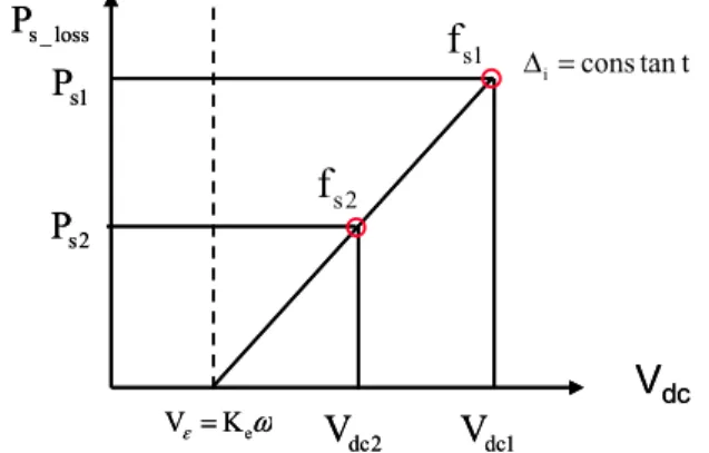
Fig. 10. Vd is the voltage across source and drain of the switch, IS1 and IS2
are switching current of switch S1 and S2, and IL is the phase current of the
motor.
V
dc loss _ sP
ω ε Ke V = 2 dcV
V
dc1 1 sP
2 sP
V
dc loss _ sP
ω ε Ke V = 2 dcV
V
dc1 1 sP
2 sP
1 sf
2 sf
t tan cons i= ΔFig. 11. The relationship between bus voltage Vdc and switching loss under
the restriction that the current ripple i
Δ is the same.
Fig. 11 shows the results of the above equations, and we can understand that when the system is operated in steady speed, switch conduction loss is decreased via decreasing VOPFC output voltage or even instruct the system to work in PAM mode. On the contrary, the bus voltage is increased to improve current response when the system needs to accelerate. Required frequency modulation is realized by the usage of DSP 2407A micro-controller, which allows rapid variation of operation frequency. The hysteresis comparison look-up table of operation frequency for PWM modulation in different bus voltage is shown in Fig. 12.
B. Mode selection controller
The mode selection control block diagram is designed as shown in Fig. 13. If the speed error is less than the limit, it means that the motor has rotated in steady speed and the operation mode will be changed to PAM mode. In PAM operation mode, the bus voltage decreases continuously until the PWM module is full duty [9]. At this time, the output voltage of VOPFC converter is as low as the back-EMF of
motor and the switching frequency of the inverter is as low as the electric frequency of the motor. On the contrary, if the speed command varies, the speed error will be higher than the limit suddenly and the operation mode will be changed to PWM mode. VOPFC Inverter Current Controller Speed Controller Current Controller Voltage Controller 110VAC PWM/PAM Select
PWM Mode PAM Mode
Speed: 1000rpm~2000rpm Speed: 1000rpm~500rpm Vdc=50V~300V PMSM Hall Sensors (a) 50 100 200 300 500 1000 2000 Speed(rpm) Vdc(V) f s=20 kHz fs=10 kHz fs=5 kHz 50 100 200 300 500 1000 2000 Speed(rpm) Vdc(V) f s=20 kHz fs=10 kHz fs=5 kHz (b)
Fig. 12. The hysteresis comparison look- up table.
+ PWM/PAMselector M U X VOPFC M U X Inverter speed* speed Speed_err speed ε speed* Vdc*
Fig. 13. The mode selection controller for PWM or PAM.
V. SIMULATION AND EXPERIMENTAL RESULTS
The proposed digital control strategy is verified through the simulation and experiment. The experiment has been realized with a DSP controlled BLDC motor drive. A switch-mode controller is designed to ensure the VOPFC converter working stability in buck mode or boost mode.
In Fig. 14(a), the output voltage is 100V, output power is 200W, and the ripple of output voltage is limited to 10%. In Fig. 14(b) and Fig. 15, the experiment waveforms verify that the VOPFC converter works well and regulates the constant output voltage in each buck mode or boost mode. The measured power factor is 94% and the efficiency is 93%. In Fig. 16, the motor can be operated stability in different dc voltage and the VOPFC can also be operation steady under the speed changing in simulation. The rated power and rated
speed of BLDC motor utilized in the present experiment are 550W and 3000rpm. With motor speed set at 1000rpm and having consistent torque load, the motor is operated independently under 100V bus voltage, with 20 kHz or 10
kHz switching frequency for each. The phase current Ia of the
motor and the command signal Kd used to change operation
switching frequency are shown in Fig. 17. When the system is operating alternately at 100V and 300V bus voltage, the switching loss in 100V voltage can reduce half of the one in 300V voltage for the same speed of motor. The efficiency of BLDCM drive can improve about 3%.
0.0 50.00 100.00 150.00 Vin Vo 0.0 -5.00 -10.00 5.00 10.00 Lin Input voltage Output voltage Input current Buck Boost Boost 0.0 50.00 100.00 150.00 Vin Vo 0.0 -5.00 -10.00 5.00 10.00 Lin Input voltage Output voltage Input current Buck Boost Boost DBcuk DBoost Vo Vin (a) (b)
Fig. 14. (a) The simulation wave of input voltage, output voltage and the response input current. (b) The experiment wave of input voltage, output voltage and the buck and boost switching signals.
100.00 150.00 200.00 Vo Vref 0.80K 1.20K 1.60K 2.00K speed_ref S4.speed 0.0 2.00 4.00 I(La) S2.Iref/100 1.75 2.00 2.25 2.50 Time (s) 0.0 1.00 2.00 S4.Idc_ref S4.Idc
Slow down Step down 0.0 -100.00 100.00 200.00 300.00 400.00 Vo Vref 0.0K -1.00K 1.00K 2.00K 3.00K 4.00K speed_ref S4.speed 0.0 2.00 4.00 6.00 8.00 10.00 12.00 14.00 I(La) S2.Iref/100 0.0 0.20 0.40 0.60 0.80 1.00 Time (s) 0.0 -1.00 -2.00 1.00 2.00 3.00 4.00 5.00 S4.Idc_ref S4.Idc
Step up Speed up Steady
inductor current Voltage reference output voltage Speed reference BLDC speed BLDC input current 100.00 150.00 200.00 Vo Vref 0.80K 1.20K 1.60K 2.00K speed_ref S4.speed 0.0 2.00 4.00 I(La) S2.Iref/100 1.75 2.00 2.25 2.50 Time (s) 0.0 1.00 2.00 S4.Idc_ref S4.Idc
Slow down Step down 100.00 150.00 200.00 Vo Vref 0.80K 1.20K 1.60K 2.00K speed_ref S4.speed 0.0 2.00 4.00 I(La) S2.Iref/100 1.75 2.00 2.25 2.50 Time (s) 0.0 1.00 2.00 S4.Idc_ref S4.Idc
Slow down Step down 0.0 -100.00 100.00 200.00 300.00 400.00 Vo Vref 0.0K -1.00K 1.00K 2.00K 3.00K 4.00K speed_ref S4.speed 0.0 2.00 4.00 6.00 8.00 10.00 12.00 14.00 I(La) S2.Iref/100 0.0 0.20 0.40 0.60 0.80 1.00 Time (s) 0.0 -1.00 -2.00 1.00 2.00 3.00 4.00 5.00 S4.Idc_ref S4.Idc
Step up Speed up Steady
inductor current Voltage reference output voltage Speed reference BLDC speed BLDC input current (a) (b)
Fig. 16. (a) The VOPFC output voltage steady in variable speed control in simulation. (b) The motor speed response is stable in variable output voltage of VOPFC in simulation. 0 0.05 0.1 0.15 0.2 0.25 0.3 0.35 0.4 0.45 0.5 -3 -2 -1 0 1 2 0 0.05 0.1 0.15 0.2 0.25 0.3 0.35 0.4 0.45 0.5 0 2 4 6 Speed=1000rpm Speed=constant Ia Kd 0 0.05 0.1 0.15 0.2 0.25 0.3 0.35 0.4 0.45 0.5 -3 -2 -1 0 1 2 0 0.05 0.1 0.15 0.2 0.25 0.3 0.35 0.4 0.45 0.5 0 2 4 6 Speed=1000rpm Speed=constant Ia Kd 20KHz 10KHz 1 i Δ Δi2
Fig. 17. The phase current Ia of the motor and the command signal Kd used to
change operation switching frequency in experiment.
VI. CONCLUSION
This paper has proposed a dual-mode control strategy for BLDC motor drivers with power factor correction used in high-efficiency compressor applications. The output inverter stage can be operated in PAM mode or PWM mode with reduced switching frequency for efficiency optimization of the compressor motor drive to maintain a constant V/Hz ratio with specified current ripples. The proposed control scheme has been verified with a DSP-controlled VOPFC inverter motor driver and an efficiency improvement of 3% has been achieved. When the compressor drive runs in constant speed mode, the VOPFC converter can maintain a constant dc output with low input current THD during the transition between buck and boost modes. If the compressor driver runs in acceleration/deceleration mode, the dc-link voltage is controlled with a specified ramping rate. Based on the proposed control scheme, innovative PWM control schemes can be developed to improve the inverter efficiency and reduce the motor audio noise by controlling the PWM duties to achieve specified phase current profile.
REFERENCES
[1] K. S. Colby and D. W. Novotny, “An efficiency-optimizing permanent-magnet synchronous motor drive,” in Proc. 1987 IEEE IAS Annual Meeting Conf., pp. 262-268.
[2] R. Ridley, S. Kern, B. Fuld, R. Eng, and B. Creek, “Analysis and design of a wide input range power factor correction circuit for three-phase application,” in Proc. 1993 IEEE APEC Conf., pp. 299-305. [3] C. Zhou, R. B. Ridley, and F. C. Lee, “Design and analysis of a
hysteretic boost power factor correction circuit,” in Proc.1990 IEEE PESC Conf., pp. 800-807.
[4] J. Chen, D. Maksimovic, and R. Erickson, “Buck-boost PWM converters having two independently controlled switches,” in Proc. 2002 IEEE PESC Conf., pp. 734-741.
[5] M. C. Ghanem and K. Al-Haddad, “A new control strategy to achieve sinusoidal line current in a cascade buck-boost converter,” in IEEE Transactions on Ind. Electron., vol. 433, no. 3, pp. 441-445, Jun. 1996. [6] Y. Zhao, “Single phase power factor correction circuit with wide output
voltage range,” Master Thesis, Dept. Elec. and Computer Eng., Univ. Virginia, Blackburg, Virginia, 1998.
[7] F. Carichhi, F. Crescimbini, F. G. Capponi, and L. Solero, “Study of bidirectional buck-boost converter topologies for application in electrical vehicle motor drives,” in Proc.1998 IEEE Applied Power Electronics Specialists Conf., pp. 287–293.
[8] L. Balogh, “Design and application guide for high speed MOSFET gate drive circuits” Texas Instruments, Appl. Note Slup 169, 2001. [9] K. Taniguchi, T. Morizane, and S. Morimoto, “Novel PAM inverter
system for induction motor drive,” in International Journal of Electron., Special issue: Power Electronics and Drive Systems, vol. 80, no. 2, pp. 143-153, Feb. 1996. Input voltage Input current Induct current BuckBoost BuckBoost
Fig. 15. The experiment waveforms of the input voltage, the input
current, and the inductor current of the VOPFC converter when Vo is

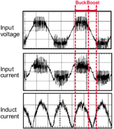
![[2015-Fall] WNFA lab1 - CamCom](data:image/gif;base64,R0lGODlhAQABAIAAAP///wAAACH5BAEAAAAALAAAAAABAAEAAAICRAEAOw==)