國
立
交
通
大
學
物理研究所
博
士
論
文
鹼金屬鹵化物奈米薄膜在共價鍵半導體表面
成長模式和電子結構
Growth Mode and Electronic Structure of Alkali Halide
Nano-Films on the Covalent Semiconductor Surfaces
研 究 生:鐘仁陽
指導教授:江進福 教授
林登松 教授
鹼金屬鹵化物奈米薄膜在共價鍵半導體表面
成長模式和電子結構
Growth Mode and Electronic Structure of Alkali Halide
Nano-Films on the Covalent Semiconductor Surfaces
研 究 生
:鐘仁陽 Student:Jen-Yang Chung
指導教授:江進福
Advisor:Tsin-Fu Jiang
林登松 Deng-Sung Lin
國 立 交 通 大 學
物 理 研 究 所
博 士 論 文
A ThesisSubmitted to Institute of Physics College of Science National Chiao Tung University in partial Fulfillment of the Requirements
for the Degree of Doctor
in Physics August 2010
Hsinchu, Taiwan, Republic of China
鹼金屬鹵化物奈米薄膜在共價鍵半導體表面
成長模式和電子結構
學生:鐘仁陽
指導教授:江進福 教授
林登松 教授
國立交通大學物理研究所博士班
摘 要
本論主要研究主題有鹼金屬鹵化物在共價鍵半導體表面和雙原子鹵素分子在半 導體表面的吸附。其中,鹼金屬鹵化物包含了氯化鈉和氯化鉀,而雙原子鹵素分子包 含了氯化碘和氯化溴氣體。所涵蓋課題包括薄膜成長的機制、原子的結構、電子特性、 在介面間電子的轉移。而我們利用分子束磊晶沉積技術和化學氣相沉積技術薄膜。氣 體-表面交互作用、吸附原子的擴散以及雙原子分子的化學吸附。實驗方法主要利用 變溫掃瞄穿遂顯微術、核心層光電子激發術及第一原理計算。結合此兩種顯微術及光 譜學的技術,便可更進一步解析表面的各種反應。 不同表面能量和晶格係數差異的大小都影響了原子結構的排列和成長模式。氯化 鈉薄膜和矽(100)-2×1 的晶格係數差異約為 5 %,而核心層光電子激發術的結果說明 了,在氯化鈉的覆蓋率小於 40 %時,部分的氯化鈉分子解離而另一部分的氯化鈉分子 直接以分子的形式吸附在表面的矽原子上形成了矽-氯-鈉的結構。掃瞄穿遂顯微術 的結果顯示,覆蓋率 65 %時,在矽表面上觀察到 c(2×2)、c(2×4)、p(2×2)等的排列 結構圖形,而這些不同的結構,主要來自於解離的鈉原子、氯原子、矽原子懸鍵以及 矽-氯-鈉的排列。當覆蓋率介於 0.65~2.25 個原子層時,在鈉、氯、氯化鈉所組成 的層面上方有著島嶼狀的氯化鈉開始成長,這島嶼狀的氯化鈉是由單位晶格長度 3.82 埃的正方形晶格所組成的,且島嶼狀的氯化鈉高度為 3.8 埃。 氯化鉀薄膜和矽(100)-2×1 的晶格係數差異為 13 %,由核心層光電子激發術的結 果說明了,在氯化鉀的覆蓋率小於一個原子層時,部分的氯化鉀分子解離。當覆蓋率 超過一個原子層時,靠近費米面的價帶電子態密度有著類似氯化鉀塊材的特徵。掃瞄圖形。當覆蓋率大於一個原子層,會出現小部分群集的氯化鉀散落在 c(4×4)的區域介 面,並且有著線條般的鏈狀。覆蓋率超過兩個原子層時,氯化鉀是一層接著一層模式 成長。結合第一原理的計算,我們可以知道這新穎的 c(4×4)結構圖形是由金字塔幾何 結構的原子所組成的。
Growth Mode and Electronic Structure of Alkali Halide
Nano-Films on the Covalent Semiconductor Surfaces
Student: Jen-Yang Chung
Advisers
: Dr. Tsin-Fu Jiang
Dr. Deng-Sung Lin
Institute of Physics
National Chiao Tung University
Abstract
This thesis studies the growth mechanism, atomic structure, electronic property, and the charge transfer at the interface between ionic solid films and covalent bonded semiconductor surface for several alkali halides and inter-halogen including NaCl and KCl, ICl, and IBr. Adsorption mechanisms, surface species, chemical reactions, atomic compositions and orderings, and film morphology during the growth using molecular beam epitaxy (MBE) and chemical vapor deposition (CVD) at room temperature were thoroughly investigated. The measurements were carried out by synchrotron radiation core level photoemission and scanning tunneling microscopy. The combination of these complimentary techniques yields much new and detailed information and understanding on the growth mode, film characteristics, and interfacial property for ionic solids on the covalent semiconductor surfaces.
Different surface energies and the dissimilar lattice mismatch lead to the different atomic structures and growth modes. For the smaller lattice mismatch (~5%) of the growth ultra-thin film of NaCl on Si(100)-2×1, the Si 2p, Na 2p, and Cl 2p core level spectra together indicate that adsorbed NaCl molecules at submonolayer coverage (θ < 0.4 ML) are partially dissociated and the rest adsorbed NaCl molecules bonded with Si to form Si-Cl-Na species. The STM results revealed that many dangling bonds are intact and form the c(2×4), c(2×2), and p(2×2) local ordered structures at the coverage of 0.65 ML. A simple model for the dangling bond ordering is presented: The different ordered structures were formed by the different arrangement of the Si-Cl-Na, dissociated Na and Cl, and dangling bonds. At 0.65 <
θ < 2.25 ML, double layer NaCl islands begin to grow on top of the Na, Cl, and NaCl mixed ad-layer. The apparent height of a NaCl double layer island is 3.8 Å and shows well-defined protrusions which are arranged into a square lattice of 3.82 Å.
The growth of KCl on the Si (100)-2×1 has a larger lattice mismatch (~13%). The Si 2p, K 3p, and Cl 2p core level spectra together indicate that adsorbed KCl molecules at submonolayer coverage also partially dissociate and that KCl nano-films above 1. 0 ML have similar features in the valance band density of states with those of the bulk KCl crystal. STM results reveal a novel c(4×4) structure at θ=1 ML. Over 1.0 ML, new clusters randomly disperse around the c(4×4) domain boundaries and often form linear chains. Further KCl deposition above 2 ML follows pseudo layer-by-layer growth. Ab initio calculations show that a model that comprises a periodic pyramidal geometry of the novel c(4×4) atomic structure is consistent with experimental results.
Acknowledgement
非常感謝我的指導老師林登松教授在這六年來對我的指導和教誨,老師對科學的 熱忱、態度,讓我看到身為一個科學研究學者,真正所應該具備的專業和精神。學生 對老師的感謝已經不是三言兩語可言盡,老師真的很謝謝您,辛苦您了。也非常感謝 口試委員江進福教授、唐述中教授、潘扶民教授、林炯源教授對於博士論文研究方面 的建議和幫助。 感謝凱銘學長、世鑫學長、明峰學長在我對實驗還懵懵懂懂的時候,認真有耐心 的教導我,帶我走進這實驗的殿堂,一直到畢業的這一刻,我還是一直覺得有你們這 些學長真好。感謝我的同學乾廷、閔光、依亭,跟你們當同窗同學,真的很開心,能 夠一起分享生活中的點點滴滴,一起熱烈的討論物理。感謝學妹曉婷,在我熬夜做實 驗的時候,會給我黑色的保肝丸。感謝學妹曉穎、欣樺、靈櫻在清大實驗室草創初期, 因為妳們的努力才有現在的實驗室。感謝我的戰友們宏道、中廷,記得在那年、這年 夏天我們在同步輻射一起努力奮鬥的日子,有你們的義氣相挺,讓我的實驗能夠順利 完成。感謝學妹盈秀在這最後的兩個月內,每天放著美麗的詩歌,抒解我緊張的情緒。 感謝學弟展源,當我在低潮時,常常你一句話,打開我心中的那個死結,讓我能夠更 有力氣的前進著。感謝學弟國威時常提供我新鮮的話題與趣事。學弟卓穎、鉦祐你們 可是實驗室的生力軍喔!加油!加油! 感謝學妹琬珩在我論文的最後階段,常常熬夜幫我分析資料,還有對我的鼓勵和 耐心,幫助我渡過這最難熬的階段,接下來新的一年,要好好加油喔,我會支持妳的。 感謝妹妹婉珍和我一起長大,有妳的陪伴,讓我學習如何當一個有責任感的好哥 哥,而妳也是一個窩心的好妹妹,常常打電話關心我的近況,找我散散心,我要將這 份喜悅跟妳分享。 最後,感激我的父親鐘富泉先生及母親郭淑惠女士,從小對我細心栽培和教導, 無怨無悔的付出,讓我能夠健康成長,順利升學。自己一人隻身從澎湖來到台灣念書 之後,仍然時時刻刻關心我和掛念著我。因為有你們的全力支持,才能讓我無後顧之 憂,專心做研究,完成博士學業,我要將這本畢業論文獻給我最親愛的父母。 一切榮耀都歸給主Contents
摘 要………...……..i
Abstract………iii
Acknowledgement ... vi
List of Figures ... x
Chapter 1 Introduction ... 1
1. 1 Motivation ... 21. 2 The Reconstructed Si(100) Surface ... 4
1. 3 Literature Review ... 10
Chapter 2 Experimental Apparatus and Methods ... 17
2. 1 The Vacuum System ... 17
2. 2 Scanning Tunneling Microscopy (STM) ... 20
2. 3 Core Level Photoemission ... 24
2. 4 Sample Preparation and Temperature Measurement ... 26
2. 5 The Tip of STM ... 28
2. 6 The evaporant of KCl and NaCl in EFM 3 ... 31
2. 7 ICl and IBr ... 35
Chapter 3 Growth mode and novel structure of ultra-thin KCl layers
on the Si(100)-2×1 surface ... 37
3. 1 Introduction ... 37
3. 2 Experiment Details ... 39
3. 3 Results and discussion ... 40
3. 3. 1 Photoemission results ... 40
3. 3. 2 STM results ... 45
3. 4 Conclusion ... 53
Chapter 4 NaCl nanofilms on Si(100) grown by MBE ... 54
4. 1 Introduction ... 54
4. 2 Experimental details ... 56
4. 3 Results and discussion ... 57
4. 3. 1 Photoemission results ... 57
4. 3. 2 STM results ... 59
4. 4 Conclusions ... 63
Chapter 5 ICl and IBr on Si(100) surfaces ... 75
5. 1 Introduction ... 75
5. 2 Experimental details ... 76
5. 3 Results and discussion ... 77
5. 3. 1 Photoemission of ICl / Si(100) ... 77
5. 3. 2 STM images of ICl on Si(100)-2×1 ... 79
5. 3. 3 STM simulation of ICl/Si(100) ... 81
5. 3. 4 Photoemission of IBr / Si (100) ... 82
5. 3. 5 STM images of IBr on Si(100)-2×1 ... 84
5. 3. 6 STM simulation of IBr/Si(100) ... 85
5. 4 Conclusions ... 86
Chapter 6 Conclusions ... 100
Appendix A In-situ study of the catalytic oxidation of CO on a
Pt(110) surface using ambient pressure X-ray
photoelectron spectroscopy ... 102
A. 1 Introduction ... 102
A. 2 Experiment Details ... 104
A. 4 Conclusion ... 111
References………..112
List of Figures
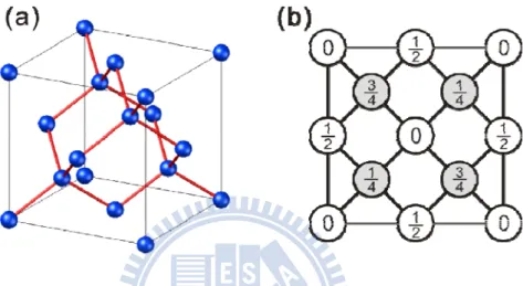
Figure 1. 1 (a) Tetrahedral bond arrangement of diamond structure. (b) The down view of diamond structure, the fractions denoted the height of the atoms in units of a
cubic edge. ... 4
Figure 1. 2 The oblique view of the ideal Si(100) surface. Spheres are Si atoms and conoid sticks are dangling bonds. Each silicon atom has two valence bonds and two dangling bonds. ... 6
Figure 1. 3 (a) The top view and (b) the side view of the ideal Si(100)-1×1 surface. ... 7
Figure 1. 4 The oblique view of the Si (100)-2×1 first layer surface structure. ... 7
Figure 1. 5 Top view (a) and side view (b) of the Si(100)-2×1 structure . ... 8
Figure 1. 6 Step structures on Si(100)-2×1 surface. (a) STM image of Si(100)-2×1 surface. The size is 15×10 nm2 and Vs = 2 V. (b) Oblique, (c) top and (d) side views of step structures. SA is the steps where the dimer rows direction on the upper terrace parallel the step edge. SB is the steps where the dimer rows direction on the upper terrace perpendicular the step edge. ... 9
Figure 1. 7 STM images (a) Large-area STM scan (1130×1130 Å2) of NaCl/Ge (100) (integral coverage about 0.15 DL). Nearly all NaCl islands have a height of one double layer (VTIP=2.7 V, IT =0.7 nA). (b) STM image (98×81 Å2) with atomic resolution of a NaCl layer of one double layer. The square lattice has a lattice constant of 4.0 Å, and is oriented along the [110] and [-110] directions of the underlying Ge (100) surface (VTIP =2.7 V, IT=1.8 nA, 1/f filter used)[4]. ... 11
Figure 1. 8 (a) Close-up (200×200 Å2) of an interesting area of Figure 1. 7(a), and (b) line scan from (a) extracted between the two arrows[4]. ... 11
Figure 1. 9 (a) An STM image after 0.4 ML LiBr deposition. 50×25 nm2. Vs = +3.3 V, IT=0.2 nA. (b) A section profile of the solid line A-A ’ in (a). (c) Rigid spheres model of single and double layer growth of LiBr. (d) Top view of LiBr dimer on Si(001) in flat-lying configuration. Thick lines mean chemical bonds between Br and Si atoms[3]. ... 12
Figure 1. 10 STM images of KI on Si(111) surface. (a) The image (30×30 nm2) obtained with VS=3.0 V and IT=0.08 nA at 0.1 ML of KI. (b) The image (20×20 nm2)
obtained with VS=3.0 V and IT=0.15 nA at 0.3 ML of KI[5]. ... 13
Figure 1. 11 STM images of KI adsorbates on Si(100) surface. (a) The image (25×25 nm2) was obtained with VS=2.0 V and IT=0.15 nA at 0.4 ML of KI. (b) The image (167×167 nm2) was obtained with VS=3.5 V and IT=0.15 nA at 0.8 ML[5]. ... 13
Figure 1. 12 STM patterns of imaging size 20×20 nm2. (a) The clean Si(100)- 2×1 surface. VS=-2.2 V, IT=0.1 nA. (b) The surface with 0.2 ML LiF. VS=-2.8 V, IT=0.2 nA. (c) The surface with 0.8 ML LiF. VS=2.8 V, IT=0.08 nA[6]. ... 14
Figure 1. 13 STM constant current topographs of Al(111) after adsorption of 0.35 ML Na and a dose of Cl2 corresponding to 0.2 ML. (a) 50×50 nm2, -1.2 V, 0.06 nA. (b) NaCl(111) island with atomic resolution (7×7 nm2, -1.2 V, 0.3 nA). (c) Structure model of an NaCl(111) island[10]. ... 15
Figure 1. 14 (a) The Cl ions of a NaCl island (appearing as protrusions, right) are located above the intrinsic steps of the substrate surface (left) as indicated by the dashed line; image size 40×18 Å. (b) Electron bombardment creates single Cl vacancies (circle); size 38×18 Å. (c) A single layer of NaCl shows alternatingly a c(2×2) and a p(1×1) structure; size 88×27 Å. (d) Defects are observed (dotted lines), which consist of two neighboring Cl ions that appear darker due to a missing Cu atom underneath; size 62×19 Å[11]. ... 16
Figure 2. 1 The UHV system of VT-STM. ... 18
Figure 2. 2 The vacuum system for core-level-photoemission spectroscopy. ... 19
Figure 2. 3 Schematic diagram displays the essential elements of STM ... 20
Figure 2. 4 Wave function Ψ(z) for an election with kinetic energy E = U/2 penetrating a potential barrier U. ... 21 Figure 2. 5 STM images of the Si-Si dimers, imaged with (a) Vs = -2.2 V and (b) Vs =
+2.6 V. The filled and empty states of these highly ordered dimmers can be probed by biasing the surface in the opposite directions. The dimensions of the
figure are 2.3 nm × 2.3 nm. ... 23 Figure 2. 6 Schematic for the energy levels in the core-level photoemission. ... 25 Figure 2. 7 A chart of the sample current vs. corresponding temperature. ... 27 Figure 2. 8 The sketch of the etching procedure for the tungsten tip. The tungsten wire is electrochemically etched to produce atomic tips. A tungsten wire is vertically inserted in a solution of NaOH as the anode. A cylindrical stainless steel is also inserted in this solution as the cathode. A positive bias is placed on the tungsten wire. ... 29 Figure 2. 9 SEM images of tungsten tip. (a) Macrostructure of a 0.5 mm diameter wire
after electrochemical etching with DC current. (b) A 0.5 mm diameter wire after electrochemical etching with AC current. ... 30 Figure 2. 10 Omicron STM tip holder. ... 30 Figure 2. 11 The evaporator EFM instrument of (a) outside view and (b) mounting a
crucible. ... 33 Figure 2. 12 The dimension of crucibles. ... 34 Figure 2. 13 experimental setup for the ICl. ... 36
Figure 3. 1 (a) Si 2p and (b) Cl 2p core level photoemission spectra (circles) of Cl-Si(100)-2×1 surface and Si(100) surface with various amounts of deposited KCl, as labeled. The solid curves are fits to the spectra. The curves labeled B, S, I and Si+ are the results of decomposition of the Si 2p spectra into contributions from the bulk, the clean surface, the interface layer and the Si-Cl species, respectively. The Cl 2p spectra at sub-monolayer coverage have two components Cl1 and Cl2. The energy zero in (a) refers to the 2p3/2 bulk position. To eliminate the band bending effect, the relative binding energy for the Cl 2p refers to the corresponding Si 2p3/2 line of the B component in (a). Dashed lines through the B, S, and Si+ components are guides for the eye. ... 42 Figure 3. 2 Integrated photoemission intensities of Si 2p, Cl 2p and K 3p as functions of
measured at KCl coverage of 1 ML. Si 2p is normalized to the clean surface before KCl deposition. ... 43 Figure 3. 3 Valence band region of Si(100) surface with various KCl coverage, as
indicated. As in Figure 3. 1(b), the relative binding energy refers to the corresponding Si 2p3/2 line of the B component in Figure 3. 1(a). Vertical dashed lines are a guide to the eye to show the general trend in the binding energy shifts of K 2p and Cl 3p. ... 44 Figure 3. 4 STM images of coverage evolution with deposition of (a) 0.1, (b) 0.3, (c) 0.5, (d) 0.8 and (e) 1.2 ML KCl on Si(100)-2×1 surface. The sample bias was -2.4 V. The images cover an area of about 40×20 nm2. The white arrows indicate the dimer-row direction in the top silicon layer. (f) Apparent topographic height profile along the green line in (e) from lower-left to upper-right. B: position of one Cluster B. ... 48 Figure 3. 5 Large-area STM images of coverage evolution with deposition of (a) 0.6, (b)
1.2, (c) 2.4 and (d) 3.6 ML KCl on the Si(100)-2×1 surface. The sample bias was -2.4 V. In (d), two substrate steps (0.14 nm in height) in the lower-left and upper-right corners remain discernible. (e) Schematic showing KCl films (orange) of several layers thick has a bulk-like structure on Si(100). Two atomic steps with heights of 0.315 and 0.14 nm show the interlayer spacings for KCl(100) and Si(100), respectively. (a), (b) and (c) cover an area of 200×100 nm2 and (d) covers an area of 300×150 nm2. ... 49 Figure 3. 6 Apparent topographic height profiles (a) and (b) (from left) along lines marked in Figure 3. 5 c and d, respectively. ... 50 Figure 3. 7 (a) Close-up image of c(4×4) structure extracted from Figure 3. 5b. Pink
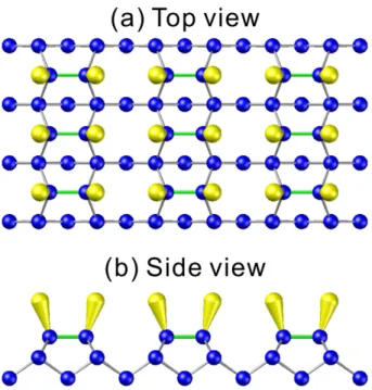
dashed rectangle denotes unit cell of ordered Cluster A. Bright protrusions on lower area are Cluster B. (b) Top view, (c) perspective view, and (d) (1,1,0) projection of atomic model of c(4×4) structures. Blue, green and purple circles represent Si, Cl and Na atoms, respectively. ... 52
Si (100) surface with various amounts of NaCl deposition, as specified. The solid curves are fits to the spectra. The curves labeled B, S, I and Si+ are the results of the decomposition of the Si 2p spectra into contributions from the bulk, the clean surface, the interface layer and the Si-Cl species, respectively. The energy zero in (a) refers to the 2p3/2 bulk position. To eliminate the band bending effect, the relative binding energy of the Cl 2p and Na 2p corresponds to the Si the 2p3/2 bulk position in (a). Dashed lines through the B, S, and Si+ components are guides for the eye. ... 64 Figure 4. 2 (a) Evolution of the components S, S+, and I intensity of the Si 2p photoemission spectra of Figure 4. 1 (a). The intensity of S+ is normalized to the component of S+ of the Cl2 terminated Si(100)-2×1. The intensity of S is normalized to the component of S of the clean Si(100)-2×1 surface. (b) Integrated photoemission intensities of Si 2p, Cl 2p, and Na 2p as functions of NaCl coverage. Data for Cl 2p and Na 2p are normalized to the intensity measured at NaCl coverage of 1 ML. Si 2p is normalized to the clean surface. The dashed and the solid lines are simple guides. ... 65 Figure 4. 3 (a) STM images of 0.1 ML NaCl on Si (100) with Vs = -1.8 V. (b) the STM
image roomed in from Figure 4.3 (a). ... 66 Figure 4. 4 Filled-state STM images showing coverage evolution with deposition of (a)
0.65, (b) 0.95, (c) 1.55, and (d) 2.25 ML NaCl on Si(100) surface as labeled. All images are obtained at room temperature with IT = 0.23 nA and Vs = (a) -2.05, (b) -2.3, (c), and (d) -2.8. The images cover an area of about (a) 80×40 nm2, and (b)-(d) 300×150 nm2. Apparent topographic height profiles along the color line are shown in Figure 4. 5. ... 67 Figure 4. 5 shows the apparent topographic height profiles and corresponding schematic
of NaCl films (large yellow rectangles) of one or two layers thick on Si(100) along the arrows in (a) Figure 4. 4 (a), (b) Figure 4. 4 (b), and (c) Figure 4. 4 (c) respectively. The apparent layer thickness of double- layer NaCl films are about 0.38 nm. The NaCl clusters and dissociated species dispersed on the Si(100) surface are represented by concave boxes of the top Si surfaces. ... 68 Figure 4. 6 (a) 20.0×10.0 nm2 STM images of Si(100) after 0.6ML NaCl deposited on
Si(100) at sample temperatures of 300 K. Solid boxes enclose selected area with (b) p(2×3), (c) c(2×2), and (d) p(2×2). (e)-(g) Schematic diagram of the area: yellow circles indicated dangling bond, green circles indicated adsorbed Cl, and blue circles with green circles at the center indicated that Na-Cl or Na--Cl. Sample bias voltages used were -2.05 V (a,b,c,d). The distance between two dimer rows is 7.68 Å. The white arrows indicate the dimer row direction. ... 69 Figure 4. 7 Sphere model of the top view for fig. (b), (c), and (d). The pattern of (a)
p(2×4), (b) c(2×2), and (d) p(2×2) correspond Figure 4. 6 (b), (c), and (d) respectively. The smallest (blue), middle (yellow), and largest (green) spheres in the topmost layer are Na, dangling bond, and Cl atoms, respectively. The woods notation is only considered the arrangement of the dangling bonds. ... 70 Figure 4. 8 (a) 10×5 nm2 STM image with atomic resolution on top of an isolated island on the same surface as Figure 4. 4(c). The sample voltage was -2.8V. Atomic structure (b) side view and (c) top view. ... 72 Figure 4. 9 Filled state STM topography (200×100 nm2) with different sample bias of the 0.9 ML NaCl deposited on Si(100), IT = 0.23 nA (a) Vs = -2.3 V and (b) Vs = -2.5 V. (c) Apparent topographic height profiles (from left) along lines marked in (a) and (b), respectively. ... 73 Figure 4. 10 STM images of NaCl deposited on Si(100) surface. (a) The image (200×100 nm2) was obtained with IT = 0.23 nA and Vs = -2.3 V at 0.9ML. (b) The zoomed-in image (80×40 nm2) is obtained from the solid box enclose selected area in (a). In (b) beside the NaCl islands, the atomic pattern as described in Figure 4. 6 was observed. ... 74
Figure 5. 1 (a) Si 2p and (b) I 4d (c) Cl 2p core level photoemission spectra (circles) of ICl–Si(100)-2×1 surface and Si(100) surface with various amounts of exposed ICl, as labeled. The solid curves are fits to the spectra. The curves labeled B, S, S’, and C are the results of decomposition of the Si 2p spectra into contributions from the bulk, the clean surface, and the Si–ICl species,
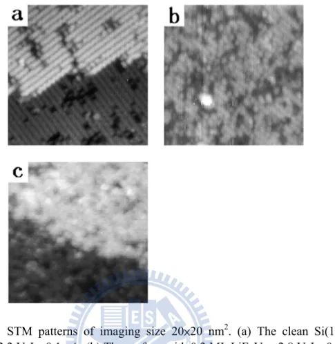
respectively. The apparent exposure in Langmuir (1 L=10-6 Torr‧s) is used as the relative measurement of ICl dosage on the bare Si(100)-2×1 surface. ... 87 Figure 5. 2 Plot of the ratio between Cl 2p, Br 3d, and I 4d core-level peak intensities as a function of ICl and IBr dose. The dada of ICl/Si(111) is from [39], IBr/Si(111) is from [38], and HCl/Si(100) is from [40]. ... 89 Figure 5. 3 The (20×10 nm2) STM images of Si(100) after saturation dosage of ICl at
room temperature. The image is obtained at room temperature with IT = 0.2 nA and VS = +2.1 V. The bright spots are I atoms, dim spots are Cl atoms, and darkest spots are defect. The white arrows indicate the dimer-row directions in the top Si layer. ... 90 Figure 5. 4 (a) Close-up image of c(2×2) structure extracted from Figure 5. 3 dash
square denotes unit cell. (b) (-110) projection of atomic model of c(2×2) structure. (c) Top view. Orange, green, and purple circles represent Si, Cl, and I atoms, respectively. According the ab-initio calculation, the bonding lengths of Si-I, Si-Cl are 2.47 Å and 2.07 Å, respectively. The ab-initio radius of I and Cl are 1.27 Å and 0.89 Å. ... 92 Figure 5. 5 For c(2×2) the empty states of the simulation STM images for the saturation
ICl on Si(100) surface above the top ICl overlayer by 1.5 Å with different sample bias at (a) +2.0 V, (b) +2.5 V, and (c) +3.0 V. ... 93 Figure 5. 6 IBr on Si(100) (a) Si 2p and (b) I 4d (c) Br 3d core level photoemission spectra (circles) of IBr–Si(100)-2×1 surface and Si(100) surface with various amounts of exposed IBr, as labeled. The solid curves are fits to the spectra. The curves labeled B, S, S’, and C are the results of decomposition of the Si 2p spectra into contributions from the bulk, the clean surface, and the Si–IBr species, respectively. ... 94 Figure 5. 7 (a) 20.0 × 10.0 nm2 STM images of Si(100) after saturation dosage of IBr at
sample temperatures of 300 K. Solid boxes enclose selected area with (b) p(4×1)-m, p(2×1)-m, (c) c(4×2)-p, c(4×2)-m, and (d) c(2×2)-m. (e)-(g) Schematic diagram of the area: Large yellow circles indicated adsorbed Br, small red circles indicated adsorbed I, and white circles indicated dangling
bonds. Sample bias voltages used were + 2.4 V (a,b,c,d). The distance between two dimer row is 7.68 Å. ... 96 Figure 5. 8 Sphere model for the Figure 5. 7 (d). (a) Side view. (b)Depiction of mixed
Iodide- and Bromide-bonded Si(100)-c(2×2) where pairs of IBr alternate along and across the dimer rows. The rhombus shows the periodic boundary of the primitive cell. According the ab-initio calculation, the bonding lengths of Si-I, Si-Br are 2.47 Å and 2.24 Å, respectively. The ab-initio radius of I and Br are 1.27 Å and 1.06 Å. ... 97 Figure 5. 9 Sphere model for the Figure 5. 7 (c). (a) Side view. (b)Depiction of mixed
Iodide- and Bromide-bonded Si(100)-c(4×2) where pairs of IBr alternate along and across the dimer rows. The rhombus shows the periodic boundary of the primitive cell. ... 98 Figure 5. 10 For c(2×2) of the empty states of the simulation STM images for the
saturation IBr on Si(100) surface above the top IBr overlayer by 1.5 Å with different sample bias at (a) +2.0 V, (b) +2.5 V, and (c) +3.0 V. ... 99
Figure A. 1 The C1s, O1s and Pt4f core level spectra of the Pt(110) surface under different conditions. A: 200 mTorr CO at room temperature; B: 200 mTorr CO+200 mTorr O2 at room temperature; C: 200 mTorr CO+200 mTorr O2 at 100 ℃; D: 200 mTorr CO+200 mTorr O2 at 150 ℃. ... 108 Figure A. 2 Partial pressures of CO, O2, and CO2 at a constant temperature of 150 ℃. We controlled the CO pressure to switch the reaction from a CO rich to oxygen rich environment and vise versa. Region A: 180 mTorr O2; Region B: 140 mTorr O2+230 mTorr CO; Region C: 150 mTorr O2+14 mTorr -28 mTorr CO; Region D: 140 mTorr O2+200 mTorr CO. These regions correspond to XPS spectra in Figure A. 3. ... 109 Figure A. 3 XPS spectra at each region in Figure A. 2 (A-D): (a) C1s spectra taken at 540 eV; (b) O1s spectra taken at 800 eV; (c) Pt4f taken at 340 eV. ... 110
Chapter 1 Introduction
This dissertation is organized into six chapters. In Chapter 1, the background and motivations of this research and a review of literatures are introduced. Chapter 2 describes the sample preparation procedures and the principles and operations of the experimental apparatus. The following three chapters are presented the three major experiments with detailed results and included two major systems to discuss–ionic crystals/covalent crystal and inter-molecule/semiconductor.
For the ionic/covalent systems, chapter 3 studied heterostructure of ultra-thin KCl films on Si (100)-2 × 1. Chapter 4 studied NaCl on Si(100)-2×1 surfaces. For inter-molecule/semiconductor, in chapter 5 the major study is to understand that the adsorption of prototypical diatomic molecule, ICl (or IBr) gas is excellent framework for the gas-surface reaction of ICl (or IBr) and semiconductor surface.
Finally, in Chapter 6 research results are summarized and the conclusions are made. Appended at the end of this dissertation is the study of the catalytic oxidation of CO on a Pt(110) surface. This research was conducted when the author was supported by Advanced Light Source of Lawrence Berkeley National Laboratory in USA in 2007. The experiments were carried out by the in-situ ambient pressure X-ray photoelectron spectroscopy at beam-line 9.3.2 in Advanced Light Source of Lawrence Berkeley National Laboratory and the author was instructed by the beam-line scientists of Zhi Lui and Bongjin Simon Mun in 2007.
1. 1 Motivation
The thin films of insulation material with wide band gap oxides and alkali halide on semiconductor or metal surfaces play an important role in microelectronic devices such as field-effect transistors, tunnel junctions, etc. With the coming miniaturization in these fields, it is not only the lateral extension of a device to be made progress, but also the thickness of insulating layer to be made smaller. As device dimensions are further reduced, the more homogeneous epitaxial system with enhanced insulation properties becomes flat necessary and crucial. The thin films of insulation material also serve well as prototypical systems for research in nano-science and nano-technology. Because the non-vanishing electron density extends through the ultrathin (thickness below 1 nm) insulating films, the scanning tunneling microscopy is a powerful tool like eyes for the investigation of the electric property and heteroepitaxial growth processes of wide-gap materials on metals or semiconductors[1, 2].
Alkali halides, such as NaCl, KI, LiF, LiBr, or CaF2, are pure ionic materials and are found to grow epitaxially on the Ge(100), Si(100), and Si(111) surfaces using STM and other techniques[3-6]. However, from previous studies that showed no atomic resolution images, we only can obtain a rough idea about their growth morphology. In my proposed research, I plan not only to obtain the growth morphology but also to grow stable and atomically thin insulating films on semiconductor surfaces with an ordered geometric structure. To achieve these goals, I need to undertake and think about what factors affect the growth mechanism.
From the basic surface science textbook, we learn that the relative energy between substrates and film and lattice mismatch are two key factors to generate three different major growth mode, namely, (a) Layer-by-Layer growth (Frank-van der Merve Mode, FM), (b) Layer-plus-Island growth (Stranski-Krastanov Mode, SK), and (c) Island growth (Volmer-Weber Mode, VW). These two factors affect each other. Therefore, in my current research I plan to vary the lattice mismatch systematically in hope to figure out the complete growth modes and mechanism of pure ionic molecule to grow epitaxially on pure covalent crystal.
An STM measurement from Glöckler et al. suggests that the growth of NaCl on Ge(100) (mismatch = 0.5%) begins with a carpet-like double-layer NaCl film[4]. For LiBr, LiF and KI on Si (100), the lattice mismatch of ionic crystals/covalent crystal are 1.3%, 29%, and 25% respectively[3, 5, 6]. The STM images showed that well ordered LiBr, LiF and KI films on Si
(100) could not be obtained at 1ML coverage. LiBr, LiF, and KI are adsorbed randomly onto Si(100), and the further growth mode follows the Volmer-Weber mechanism of island growth on Si(100) and Si(111). However, we lack the information of lattice mismatch in the midway between 1 % and 30 %. So, as the first trial, I chose the potassium chloride (KCl) and sodium chloride (NaCl) as the evaporated source. Because the heterostructure of KCl/Si(100) and NaCl/Si(100) have 15% and 5% lattice mismatch respectively, this work could help us to understand the growth mechanism of alkali halide on the group IV semiconductor surfaces.
1. 2 The Reconstructed Si(100) Surface
The Si(100) surface is used to be the substrates for my follows experiment, and its
atomic structure of surface introduced as follows. Silicon is a group in IV element with four electrons in its outer orbit and crystallize in the diamond structure with lattice constant a = 5.43 Å, as shown in Fig. 1.5. In a silicon crystal, each silicon atom has four valance bonds bonded to four neighboring silicon atoms in tetrahedral form.
Figure 1. 1 (a) Tetrahedral bond arrangement of diamond structure. (b) The down view of diamond structure, the fractions denoted the height of the atoms in units of a cubic edge.
As the Si crystal is cleaved along a different crystal orientation, the surface of Silicon reconstruct into new different surface atomic structure. For example, if the crystal is cleaved along the (100) direction, the exposure surfaces reconstruct into 2×1 structure to form a Si(100)- 2×1 structure. If the crystal is cleaved along the direction normal (111) direction, the new surface reconstruct into 7×7 structure to be called Si(111)- 7×7 surfaces. In this section, the detail of the Si(100)-2×1 structure is discussed.
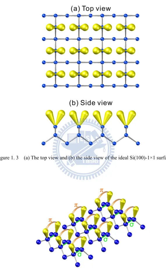
If the silicon crystal is cleaved along the (100) direction, two valence bonds of each Si atom on the exposed surface is broken and transform into dangling bonds. Therefore, every silicon atom in the surface has two dangling bonds and two valence bonds, as shown in Fig. 1.6. Figure 1.7 displays the top view of this unreconstructed Si(100) surface with 1×1 structure. In this 1×1 structure, the surface energy is high since the density of the dangling bonds is high (two dangling bonds per atoms), and then the 1×1 structure is unstable. To reduce the numbers of the dangling bonds, the first layer atoms in the surface will reconstruct. By this way, the surface energy will be lower and the surface structure will be more stable.
Upon reconstruction, two neighboring atoms form a strong sigma (σ) bond by combined one of the two dangling bonds. The top-layer atoms of the Si(100) surface dimerize (as two surface atoms binding together to form a dimer) to reduce the number of dangling bonds. These bonded pairs of Si atoms are called dimers. The amount of dangling bonds is reduced by 50 %. This establishes two characteristic directions on the surface, along the dimer row and perpendicular to the dimer. The parallel rows of the dimer bonds also reduce the overall surface energy. These remaining dangling bonds can further form a weak pi (π) bond, as shown in Fig. 1.8. Then the 1×1 structure of the surface have transformed into 2×1 structure, as shown in Fig. 1.9, to be a stable surface.
When preparing the Si(100) surface, the step structure formed by the cleavage along the (100) direction, as shown in Fig. 1.10. The height of the step is about 1.36 Å. The dimer rows on the neighboring terraces are perpendicular, so steps of the terraces divide into two types. SA is the steps where the dimer rows direction on the upper terrace parallel the step edge. SB is the steps where the dimer rows direction on the upper terrace perpendicular the step edge.
Figure 1. 2 The oblique view of the ideal Si(100) surface. Spheres are Si atoms and conoid sticks are dangling bonds. Each silicon atom has two valence bonds and two dangling bonds.
Figure 1. 3 (a) The top view and (b) the side view of the ideal Si(100)-1×1 surface.
Figure 1. 6 Step structures on Si(100)-2×1 surface. (a) STM image of Si(100)-2×1 surface. The size is 15×10 nm2 and Vs = 2 V. (b) Oblique, (c) top and (d) side views of step structures. SA is the steps where the dimer rows direction on the upper terrace parallel the step edge. SB is the steps where the dimer rows direction on the upper terrace perpendicular the step edge.
1. 3 Literature Review
Ultrathin well ordered alkali halide layers have been grown successfully and subsequently studied by STM on various substrates, including germanium, aluminium, copper and silver surfaces.
NaCl islands have indeed been successfully grown on numerous crystalline metal surfaces, such as Cu(111), Cu(110), Cu(311), Ag(111), Ag(100), Al(111), and Al(100)[1, 7-10].
STM studies of alkali halide thin films grown on semiconducting substrates have been carried out for the systems; NaCl/Ge(001),LiBr/Si(001),LiF/Si(001),and KI/ Si(001)[3, 4, 6].
In a study on the initial growth of NaCl overlayers on Ge(100), Glöckler et al reported STM images for NaCl films up to a thickness of three atomic layers in Figure 1. 7, giving evidence for the earlier proposed carpet-like growthmode of the NaCl layer overmonatomic Ge steps, even for small NaCl islands at submonolayer coverage. The authors report that they were only able to perform STM images by imaging occupied sample states using tip voltages of U=1.5–2.7 V. The authors discuss their observation of lateral atomic resolution for the initial double layer[4].
As UPS data indicate that the band structure of the NaCl double layer, at least for k parallel to the surface, is similar to that of the bulk, with the valence band maximum at about 4.2 eV, Glöckler et al concluded that the tunnelling current is most likely predominantly due to emission from Ge states through the NaCl layer. They suggest therefore that the lateral contrast, showing protrusions at either the Na+ or the Cl− positions, is due to a perturbation and interaction of the Ge wavefunction(s) by the NaCl layer causing a lateral variation of the tunnelling barrier. In Figure 1. 8, the reported apparent heights of the NaCl layers on Ge(001) are positive, but smaller than the corresponding geometric heights (3.8±0.3 Å versus 5.6 Å for the first (double) layer and 2.0±0.3 Å for the second (single) versus 2.8 Å NaCl layer)[4].
Figure 1. 7 STM images (a) Large-area STM scan (1130×1130 Å2) of NaCl/Ge (100) (integral coverage about 0.15 DL). Nearly all NaCl islands have a height of one double layer (VTIP=2.7 V, IT =0.7 nA). (b) STM image (98×81 Å2) with atomic resolution of a NaCl layer of one double layer. The square lattice has a lattice constant of 4.0 Å, and is oriented along the [110] and [-110] directions of the underlying Ge (100) surface (VTIP =2.7 V, IT=1.8 nA, 1/f filter used)[4].
Figure 1. 8 (a) Close-up (200×200 Å2) of an interesting area of Figure 1. 7(a), and (b) line scan from (a) extracted between the two arrows[4].
LiBr/Si(001) heterostructure has been investigated by scanning tunneling microscopy and spectroscopy (STM and STS). In the initial stage of LiBr growth, rectangular islands are observed consisting of accumulation of about 0.2 nm-thick unit layers. The STM results
indicate that LiBr grows on Si(001) in a single layer fashion. The STS measurement shows a wide band gap region in I-V curve and the energy gap of the LiBr film shows no thickness dependence down to a nominal thickness of 1.2 monolayer (ML)[3].
Figure 1. 9 (a) An STM image after 0.4 ML LiBr deposition. 50×25 nm2. Vs = +3.3 V, IT=0.2 nA. (b) A section profile of the solid line A-A ’ in (a). (c) Rigid spheres model of single and double layer growth of LiBr. (d) Top view of LiBr dimer on Si(001) in flat-lying configuration. Thick lines mean chemical bonds between Br and Si atoms[3].
The growth of submonolayer KI on Si(111) and Si(100) surfaces at room temperature has been studied with ultrahigh vacuum scanning tunneling microscopy (STM). The STM results show that KI on these surfaces essentially follows island-growth with a reactive interface, and that the morphology of the KI adsorbates at submonolayer coverage critically depends on the atomic structure of the surfaces. On the Si(111) surface, KI initially (coverage below 0.4 monolayer) Tends to coalesce into clusters of size smaller than the 7×7 unit-cell. With further deposition the clusters grow into well-defined islands. On the Si(100) surface, the KI initially shows dissociative adsorption; distinctive islands appear with coverages above 0.4 monolayer, preferentially clustering at the steps and growing into islands with less regularity of size and shape. This comparative study enables us to evaluate the effects of the adsorbate–substrate and adsorbate–adsorbate interactions on the adsorbing behavior and the morphological evolution of the KI/silicon systems[5].
Figure 1. 10 STM images of KI on Si(111) surface. (a) The image (30×30 nm2) obtained with VS=3.0 V and IT=0.08 nA at 0.1 ML of KI. (b) The image (20×20 nm2) obtained with VS=3.0 V and IT=0.15 nA at 0.3 ML of KI[5].
Figure 1. 11 STM images of KI adsorbates on Si(100) surface. (a) The image (25×25 nm2) was obtained with VS=2.0 V and IT=0.15 nA at 0.4 ML of KI. (b) The image (167× 167 nm2) was obtained with VS=3.5 V and IT=0.15 nA at 0.8 ML[5].
The surface morphology of Si(100)- 2×1 with submonolayers of LiF adsorbate and its annealing behavior are studied using scanning tunneling microscopy. LiF adsorbs randomly on the Si(100)-2×1 surface at room temperature (RT), and the 2×1 structure disappears when the coverage of LiF is close to 1 monolayer. Interaction of the Si surface and the LiF adsorbate is enhanced by specimen annealing, which causes dissociation of the LiF and fluorination of the Si surface. Desorption of SiFx (x=1, 2, 3, 4) results in surface etching. After annealing at 700℃ for 5 min, fluorine on the surface x decreased below the limit of
the detection by X-ray photoelectron spectroscopy, and the Si surface is reconstructed to 2× 1 at about 800℃[6].
Figure 1. 12 STM patterns of imaging size 20×20 nm2. (a) The clean Si(100)- 2×1 surface. VS=-2.2 V, IT=0.1 nA. (b) The surface with 0.2 ML LiF. VS=-2.8 V, IT=0.2 nA. (c) The surface with 0.8 ML LiF. VS=2.8 V, IT=0.08 nA[6].
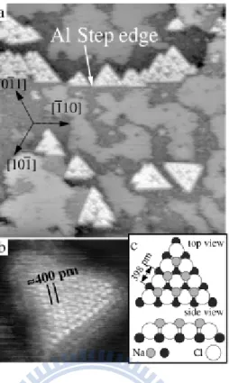
A carpet-like growth mode of NaCl at submonolayer coverage is also found on the aluminium, copper and silver substrates. Atomic resolution images of the NaCl(001) layers on all of these substrates also show a periodicity that corresponds to the positions of one type of ion. The NaCl islands appear for all of these substrates, also with positive apparent height in the STM images. For ultrathin insulating NaCl layers on Al(111) and Al(100), atomic resolution has been obtained at negative sample bias voltages (−0.5 to −3.0 V), imaging the Cl anions as confirmed by spatially resolved ab initio calculations of the local density of states. Decreasing NaCl–NaCl step heights were observed with increasing layer thickness and a maximum thickness of three layers for successful imaging was inferred. However, the gap width of the NaCl films has not been investigated. Apart from the energetically favoured (001) orientation of the NaCl layers, Hebenstreit et al reported recently on the growth of polar NaCl islands on Al(111)[10].
Figure 1. 13 STM constant current topographs of Al(111) after adsorption of 0.35 ML Na and a dose of Cl2 corresponding to 0.2 ML. (a) 50×50 nm2, -1.2 V, 0.06 nA. (b) NaCl(111) island with atomic resolution (7×7 nm2, -1.2 V, 0.3 nA). (c) Structure model of an NaCl(111) island[10].
NaCl on Cu(111) has been studied by Repp et al. Similar to the observations on Ge and Al substrates, the islands are imaged with bright contrast in STM images. Atomic resolution images show, even for bias voltages within the band gap of bulk NaCl, the square lattice corresponding to one type of ion of NaCl(001). dI/dU measurements on the NaCl films show a shift of the prior Cu(111) surface state onset towards higher energies upon adsorption of NaCl which is interpreted as an interface state due to NaCl adsorption[11, 12].
In a recent paper, the adsorption properties of NaCl monolayers and bilayers adsorbed on Cu(311) and Cu(100) have been also investigated theoretically by Olsson et al using density functional calculations. These investigations include the calculation of adsorption energies and workfunctions for adsorbed NaCl monolayers and bilayers and are compared to the experimental observations of NaCl layers on copper surfaces. For the Cu(311) surface a direct covalent interaction between Cl 3p and Cu 3d states has been identified.
Figure 1. 14 (a) The Cl ions of a NaCl island (appearing as protrusions, right) are located above the intrinsic steps of the substrate surface (left) as indicated by the dashed line; image size 40×18 Å. (b) Electron bombardment creates single Cl vacancies (circle); size 38×18 Å. (c) A single layer of NaCl shows alternatingly a c(2×2) and a p(1×1) structure; size 88×27 Å. (d) Defects are observed (dotted lines), which consist of two neighboring Cl ions that appear darker due to a missing Cu atom underneath; size 62×19 Å[11].
Chapter 2 Experimental Apparatus and Methods
2. 1 The Vacuum System
The STM experiment was conducted in an ultrahigh-vacuum (UHV) system. The main chamber is equipped with a variable-temperature scanning tunneling microscopy (VT-STM, Omicron), a manipulator, a pumping system, gas sources including H2, Cl2 and HCl, as shown in Fig. 2.1. The pumping system is consisting of a dry pump, a turbo pump, a titanium sublimation pump (TSP), and an ion pump. The base pressure of this vacuum system is 1×10⁻¹⁰ torr.
The dry pump is used first to lower pressure in the vacuum chamber to ~10-3 torr. Then the turbo pump automatically starts to lower the pressure to the 10-6 torr range. At this lower pressure, the ion pump turns on. As the pressure drops to ~10-7, we start to bake the chamber at about 120 °C for over 24 hours. After the chamber cools down to RT, we gain the ultra-high vacuum about 1×10⁻¹⁰ torr.
The core-level-photoemission experiment is carried out at the National Synchrotron Radiation Research Center (NSRRC) located in the Hsin-chu Science-based Industrial Park, Taiwan. Light from the 1.5-GeV storage ring was dispersed by a Dragon-type 6-m wide range spherical grating monochromator (SGM). This beamline has two energy range, i.e. 10-175 eV from a low energy branch and 120-1500 eV from a high energy branch. In our experiment, we use the high energy branch since the main photon energies used are 140, and 240 eV. All the adsorptions of H, Cl and HCl were prepared in situ in the ultra-high vacuum system, as shown in Fig. 2.2. In the photoemission experiment, the procedure to obtain the ultra-high vacuum is the same as the STM experiment.
2. 2 Scanning Tunneling Microscopy (STM)
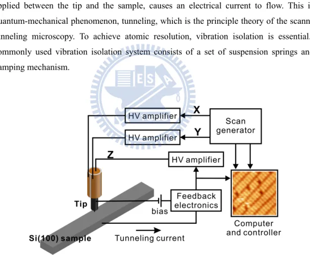
Since Binnig et al. invented the Scanning Tunneling Microscopy (STM) and obtain the atomic resolution in 1982, the STM technique has been widely used in various fields, like condensed-matter physics, chemical, biology physics and etc. Especially, after resolving the structure of the Si(111)-7×7 in real space using STM , this instrument has proved to be an extremely powerful tool.
Figure 2.3. displays its essential elements. A probe tip, usually made of tungsten (W) or Pt-Ir alloy, is attached to a piezoelectric scanner. Using the coarse positioner and the z piezo, the tip and the sample are brought to within a few angstroms of each other. A bias voltage, applied between the tip and the sample, causes an electrical current to flow. This is a quantum-mechanical phenomenon, tunneling, which is the principle theory of the scanning tunneling microscopy. To achieve atomic resolution, vibration isolation is essential. A commonly used vibration isolation system consists of a set of suspension springs and a damping mechanism.
The operating principle of the STM is based on the quantum mechanical phenomenon of tunneling. In this section, we discuss the concept of the tunneling through one-dimensional model. First we consider the classical situation. In the classical mechanics, an electron with energy E moving in a potential U(z) is described by
2 ( ) 2 Z p U z E m …………...………...……….……..(2.1)
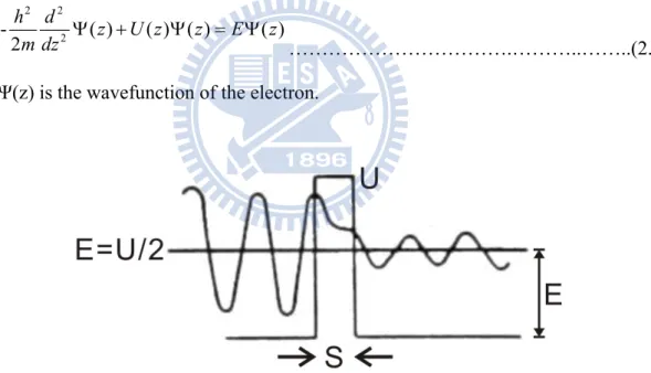
In the regions where E > U(z), the electron has a nonzero momentum Pz. It means that the electron has the ability to be in those regions. Otherwise, in the regions where E < U(z), the electron can not penetrate into those regions. In other words, the electron with energy E has no possibility to be find in the regions with U(z) >E. Now we discuss the quantum effect. In the quantum mechanics, the motion of the same electron is described by the Schrödinger’s equation, 2 2 2 - ( ) ( ) ( ) ( ) 2 h d z U z z E z m dz ……….………..……..(2.2)
Ψ(z) is the wavefunction of the electron.
Figure 2. 4 Wave function Ψ(z) for an election with kinetic energy E = U/2 penetrating a potential barrier U.
For a electron with E = U/2 incident on a square barrier from the left, as shown in Fig. 2.4. The Schrödinger’s equation of this electron
0 (z) U 2 1 (z) 2 2 2 2 dz d m ………..(2.3) has the solution:
(z) ...( 0) (z) ...(0 ) (z) ...( ) ikz ikz Kz Kz ikz Ae Be z Ce De z s Fe z s ………..(2.4) where 2 1 ) 2 ( mU k ; 2 1 ) (mU K
Eq. (2.4) can be solved for the transmission coefficient T = |F/A|2 by matching of the boundary conditions on Ψ and dΨ/dz at x = 0 and x = s. That is
Ks Kk K k T 2 2 2 2 sinh ) 2 ( 1 1 ……….(2.5)
Because a barrier of width s that is much thicker than the wave function decay length of 1/K, KS >> 1, the transmission coefficient can be approximated as
ks e K k K k T 2 2 2 2 2 ) ( 16 ………....(2.6) It is this exponential dependence of the transmission coefficient T on the barrier width s that enables atomic resolution images in tunneling microscopy. It provides a sufficient signal, the tunneling current, for atomic scale feedback control of the gap width s along the z direction.
Interestingly, use of 1° miscut Si(100) single-crystal wafers allows for highly rotationally oriented samples in which all the Si-Si dimers are pointed in the same direction, yielding anisotropic surfaces on a centimeter length scale. The high ordering of the dimers, showing both the filled and empty states, is shown in the stunning STM images of Fig. 2.5; the filled and empty states were imaged by changing the tip bias.
Figure 2. 5 STM images of the Si-Si dimers, imaged with (a) Vs = -2.2 V and (b) Vs = +2.6 V. The filled and empty states of these highly ordered dimmers can be probed by biasing the surface in the opposite directions. The dimensions of the figure are 2.3 nm × 2.3 nm.
2. 3 Core Level Photoemission
The core level photoemission experiment is to collect the photoelectrons excited from core level near nucleus. Photoelectrons were collected and analyzed by a large hemispherical analyzer. By measuring the variation of the photoelectron kinetic energy, we can observe the species of the passivated atoms and chemical bonding etc.
The photoelectrons are excited from inner energy levels (binding energy >20 eV), of which the orbital radius is less than 0.3 Å. In solid state, the core level wave functions are independent such that the binding energies of the atoms in bulk are the same. However, the potential of the atoms near surface becomes different because the local atomic environment changes. The potential difference of surface atoms results in chemical shift of the core level binding energy.
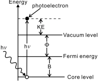
We can explain the relationship between the kinetic energy (KE) of excited photoelectrons and energy of incident photons by the energy conservation law as Eq. 2.7. The relation of the energies is shown in Fig. 2.6.
KE=hν-B-Φ
………(2.7) KE : kinetic energy of excited photoelectron
hν: photon energy B: binding energy Φ: work function.
In this formula, the binding energy B is the difference between the core level and Fermi level. The work function Φ is the difference between the Fermi level and vacuum level. This formula is based on the ideal situations; however, we have to consider other factors like secondary electrons and escape depth etc. The escape depth of the excited photoelectron is dependent on the kinetic energy, in other word, the higher kinetic energy, the larger escape depth. Therefore, the escape depth of photoelectrons of kinetic energy 20 eV ~ 110 eV is less than 10 Å. The spectra obtained by analyzing these photoelectrons provide us the message of the surface.
Figure 2. 6 Schematic for the energy levels in the core-level photoemission.
After electrons excited from core level, left holes will be occupied by other electrons. The reaction of occupation can occur in two processes. First, the electrons in the higher energy level occupy the left holes and release the photons of energy equivalent to the difference between two levels. Next, the electrons in the higher energy level occupy the electron holes and release energy. The released energy is not carried by photons but directly excites electrons to leave surface. The excited electrons in the second process are so-called Auger electrons. The Si 2p and Ge 3d core level photoemission is mainly contributed from Auger electrons.
The lifetime of the electron holes yields Lorentzian broadening. The other factor to result in broadening spectra is the resolution of the analyzer, which produces a Gaussian width of the spectra. The convolution of the Lorentzian width and Gaussian width yields a Voigt lineshape for the spectra.
2. 4 Sample Preparation and Temperature Measurement
Various sample treatments will be conducted depending upon the type of the sample that will be required for the experiment. The Si(100) samples used in our experiment were sliced up into pieces of size 1×8 mm2 from a antimony (Sb) doped wafers with a dopant concentration of approximately 1.5×1015 cm-3. The misalignment of the wafer is about 0.1 degrees. Before loading the samples into the vacuum chamber, we blow off the dust on the surface of the samples with pure nitrogen gas so we don’t have unwanted particles on the surface of the samples which could affect our measurements. After loading the samples to the UHV chamber, the samples are then being degassed for over 12 hours at ~900 K using a small AC current. After degassing, the sample was flashed at ~1450 K for a few seconds in order to remove the oxide layer on the surface and form a dimerized clean Si(100)-2×1 surface.
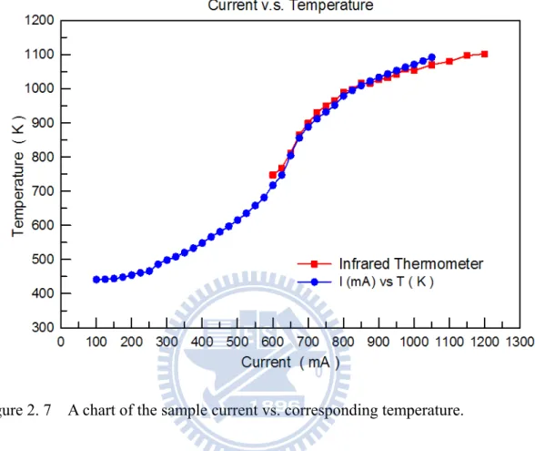
The substrate was heated by passing a controlled dc current directly through the sample. The sample temperature that corresponds to each current was obtained using an infrared optical pyrometer and calibrated by gluing a tiny type-K thermocouple to the center of the sample following the final last STM run, as shown in Fig. 2.7. The uncertainty in the temperature measurement was estimated to be approximately 5 K.
2. 5 The Tip of STM
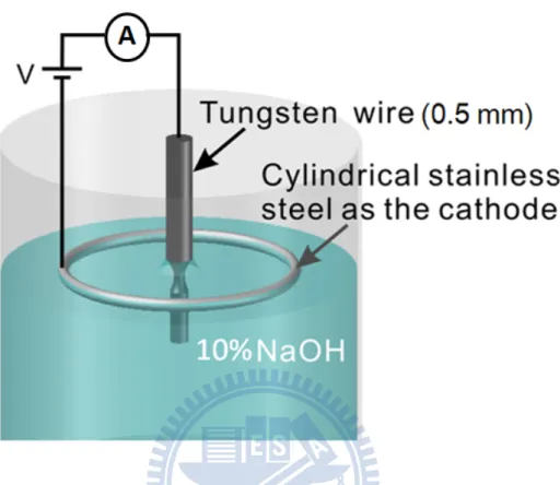
The size, shape and cleanliness of a scanning tunneling microscope (STM) tip are very important for the resolution of a STM. In the UHV system, the W tip is often used. A W tip has to be prepared by electrochemical etching.
For etching we used a tungsten wire as the anode electrode in a special design screw, a circle stainless steel was taken as the cathode, and a 2 M NaOH solution is used as the electrolyte, as shown in Fig.2. The following reactions take place.
2 2(g) 2 (s) 4 2 2 (s) 2 4 2(g) Cathode : 6H O 4e 3H 6OH Anode : W 8OH WO 4H O 6e
Total reaction : W 2OH 2H O WO 3H
…..………(2.8)
The tip was cut from straight W (purity is 99.99%) wire of 0.5mm diameter and the 6mm length (Goodfellow Ltd, England) because the diameter of the tip holder is also 0.5mm.
In order to remove the oxide layer of the surface W wires, the wires has to be slightly (about 5 seconds) electropolished over a large part of the wire in the NaOH solution with constant voltage of 15V.
The depth of wire under the surface of NaOH is about 2mm.When the tip start to etch, etching reaction is happened at the interface of the air and the solution. The power supply has constant voltage with an automatic switch-off control. During etching the current through the tip will decrease linearly with time, because the tip below the solution surface decrease and the resistance of the tip (anode) increase. After a long time, the tip forms a neck shape and become thinner and thinner. Eventually the part of the neck is cut down by the weight of the wire under the solution surface dropped down. To remove the residual NaOH solution from the tip surface the tip are then been soaked in de-ioned water for 30 minutes and cleaned by pure methanol. Finally, the tip is set in the tip holder, and backing with 120℃ in the transport chamber at P=10-8 torr, after 16 hours the tip is complete.
Figure 2. 8 The sketch of the etching procedure for the tungsten tip. The tungsten wire is electrochemically etched to produce atomic tips. A tungsten wire is vertically inserted in a solution of NaOH as the anode. A cylindrical stainless steel is also inserted in this solution as the cathode. A positive bias is placed on the tungsten wire.
Figure 2. 9 SEM images of tungsten tip. (a) Macrostructure of a 0.5 mm diameter wire after electrochemical etching with DC current. (b) A 0.5 mm diameter wire after electrochemical etching with AC current.
2. 6 The evaporant of KCl and NaCl in EFM 3
In the UHV evaporator EFM3 (Evaporator with integral flux Monitor) is made from Omicron Vakuumphysik GMBH. The NaCl evaporate is evaporated from a crucible which is made of Al2O3 (see Fig 2.). This is achieved by electron bombardment heating. The bombarding electron beam induces a temperature rise at the top of the evaporant, causing evaporation.
From appreciate crucibles low melting point, low vapor pressure or reactive material can be evaporated. The appreciate material of crucible can be made of Al2O3, pyrolytic boron nitride (pBN), grapite, tantalum, and etc. In my experiment the Al2O3 crucible is chosen for setting the NaCl of evaporant. The instrument is designed for high precision sub-mono-layer up to multi-layer deposition of a wide variety of evaporants including highly refractory materials. The fig 2. is the dimensions of Al2O3 crucibles.
An important feature of the EFM3 is the integrated flux monitor. In order to obtain the precise rate, once calibrated the flux monitor replaces the necessity of a quartz thickness monitor by continuously monitoring the evaporation rate. Flux is measured directly, which allows a much more precise rate adjustment and much faster rate control than an indirect. The beam exit column contains an ion collector which serves as a flux monitor. At a given electron emission current (IEM) and e-beam voltage the ion flux measured there is directly proportional to the flux of evaporated atoms. The ion flux is displayed on the left indicator of the electronics unit. The flux monitor also operates with the shutter closed thus allowing to preset the evaporation rate.
The EFM3 comes with an shutter at its outlet which can be opened and closed by a rotary drive. This allows precise flux adjustment prior to exposure, and exact control of the evaporation time.
The evaporation cell is contained in a water-cooled copper cylinder (cooling shroud). When NaCl is evaporated, the filament is heating and causing the background pressure increased. So the cooling shroud usefully prevents the background pressure increase too high. But this also depends on the material of evaporant and the pumping speed of the vacuum system.
IEM = 6 mA, and Ifil = 2A, was used. Eventually the molecular bean was giving about 1ML/minute. The ML is referred to the surface density of the unreconstructed Si(100) surface, i.e. 1ML = 6.8×10¹⁴/cm2.
Figure 2. 11 The evaporator EFM instrument of (a) outside view and (b) mounting a crucible.
Material Measure Ta/Mo mm pBN mm C mm Al2O3 mm SSteel mm ID 4 4.5 5.3 6 5 OD 5 or 8 8 10 10 7 L 6 7 10 14 15 Tmax (℃) 2000 1600 1400 1400 800
2. 7 ICl and IBr
Vapors of IClwere introduced into the vacuum chamber through a precision leak valve and a tube facing the sample while tips were retracted for hundreds of nanometers.
The process of Freeze-Pump-Thaw Degassing for ICl(or IBr)
(1) Place the solution of ICl(99.999%) in a glass tube shown in Figure 2. 13. Make sure the leak valve is closed. Be careful not to use more than 50% of the volume of the glass tube because overfilled the glass tube frequently shatter during this process. (2) Hook it up to the oil pump and freeze the liquid of ICl. Liquid nitrogen is usually
best for this. Before freezing make sure that the environment in the glass tube is free of oxygen to prevent condensing liquid oxygen upon freezing.
(3) When the solution is frozen, only open the valve B to vacuum and pump off the atmosphere for 10-30 minutes.
(4) Close the valve B.
(5) Thaw the solution until it just melts using a tepid water bath. You will see gas bubbles evolve from the solution of ICl. Try not to disturb the liquid. Note: Letting the frozen solution thaw by itself, or using a container of water that melts only the bottom of the frozen solution of ICl may cause the vessel to break.
(6) Replace the water bath with the cooling bath and refreeze the solution of ICl.
(7) Repeat steps (3) – (7) until you no longer see the evolution of gas as the solution thaws. The solution should be put through a minimum of three cycles.
Chapter 3 Growth mode and novel structure of ultra-thin
KCl layers on the Si(100)-2
×1 surface
This study investigates ultra-thin potassium chloride (KCl) films on the Si(100)-2×1 surfaces at near room temperature. The atomic structure and growth mode of this ionic solid film on the covalent bonded semiconductor surface is examined by synchrotron radiation core level photoemission, scanning tunneling microscopy and ab initio calculations. The Si 2p, K 3p and Cl 2p core level spectra together indicate that adsorbed KCl molecules at submonolayer coverage partially dissociate and that KCl overlayers above one monolayer (ML) have similar features in the valance band density of states as those of the bulk KCl crystal. STM results reveal a novel c(4×4)structure at 1 ML coverage. Ab initio calculations show that a model that comprises a periodic pyramidal geometry is consistent with experimental results.
3. 1 Introduction
Heteroepitaxy is frequently used to develop new synthetic materials-especially semiconductors-for fundamental research and novel devices. Heterostructures that combine very dissimilar materials, such as pure ionic compounds on pure covalent crystals [4, 13], have generated much interest recently owing to the realization of a variety of possible novel properties. Ionic crystals and covalent crystals are held together by attractive forces of very different nature. Understanding the growth mechanism of thin ionic crystals on covalently bonded group IV semiconductors and their interfacial property can broaden our knowledge of principles that govern heteroepitaxy and surface science.
NaCl/Ge(100) is a prototypical system for the heteroepitaxy of small-lattice mismatch ionic crystals/covalent crystal. The second nearest-neighbor separation R1for an NaCl crystal is 3.98 Å. The surface lattice constant a, or the period of unreconstructed Ge(100)-1 ×1, is 4.00 Å. The lattice mismatch at the heterostructure of NaCl/Ge(100) is close to 0.5%. Previous studies have established that NaCl can grow epitaxially on Ge(100) with a high degree of quality under suitable conditions [4, 14-16]. An STM measurement suggests that the growth of NaCl begins with a carpetlike double-layer NaCl film [4]. In an electron energy loss scattering (EELS) measurement Zielasek, Hildebrandt and Henzler found
electronic states at the NaCl/Ge interface and suggested that the dimerization of the Ge(100) surface is not eliminated at the NaCl/interface-even if the thickness of NaCl rises to 20 ML
[13].
For large lattice mismatch systems, the growth of alkali halide on the Si and Ge surfaces at around one monolayer coverage does not yield an ordered surface structure. For example, sub-monolayer LiBr (R1 = 3.89 Å) and LiF (R2 = 2.85 Å) are adsorbed randomly onto Si(100) (a = 3.84 Å) at room temperature [3, 6]. Guo and Souda observed that KI (nearest–neighbor separation R0= 3.53 Å) dissociatively adsorbs on the Si(100) surface at a coverage of less than 0.5 ML [5]. Although thick flat films can be obtained, the growth of KI, LiF and LiBr on Si(100) and Si(111) surfaces proceeds by the Volmer-Weber (VW) mechanism of island growth as a result of the interfacial lattice mismatch.
Potassium chloride (KCl) has the sodium chloride structure with R1= 4.32 Å. The heterostructure of KCl/Si(100) has a very large (13%) lattice mismatch. This study establishes that a single monolayer of KCl forms ordered superstructure on the Si(100) surface and the KCl film can be grown epitaxially. Based on ab initio calculations, this study demonstrates that regular arrays of four-facet pyramid-like wrinkles reduce the excess energy associated with a large lattice mismatch. In addition to its uniqueness, this new superstructure also demonstrates the interaction between a pure ionic monolayer and the surface of pure covalent crystals.
3. 2 Experiment Details
The Si(100) samples were antimony doped with a resistance of 0.01 Ωcm. After thorough outgassing at ~900 K, a dimerized clean Si(100) surface was obtained by a few seconds of heating to ~1450 K. 99.99% pure KCl was sublimated from an alumina crucible by a feedback-controlled electron bombardment beam. To minimize contamination at submonolayer coverage, the photoemission was measured immediately after KCl was deposited on clean surfaces. Above one monolayer, the deposition was often performed additively. The deposition rate was determined using an integral flux monitor that was calibrated by a quartz-crystal thickness monitor. The coverage of KCl adsorbate in ML (denoted by h), was estimated from the exposure time, assuming the sticking coefficient is 1. The ML is referred to the surface density of the unreconstructed Si(100) surface, i.e. 1 ML = 6.8×10¹⁴/cm2. The substrate temperature during growth was approximately 330 K.
The photoemission spectra were recorded at the Taiwan Light Source laboratory in Hsinchu, Taiwan. Synchrotron radiation from a 1.5 GeV storage ring was dispersed by a wide-range spherical grating monochromator (SGM). The photocurrent from a gold mesh placed in the synchrotron beam path was monitored to determine the relative incident photon beam flux. Photoelectrons were collected from 60° off normal emission and analyzed by a 125 mm hemispherical analyzer in a μ-metal-shielded UHV system with a based pressure of ~3×10⁻¹⁰ torr. The overall energy resolution was better than 120 meV. The STM measurement was taken in a separated UHV chamber with a base pressure of 8×10-11 torr. The tunneling current was about 0.1 nA. The topographic height measurement did not strongly depend on the sample bias around -2.4 V typically used.