行政院國家科學委員會補助專題研究計畫 ■ 成果報告
□期中進度報告
以氫化物氣相磊晶法開發III-V 族氮化物基板
計畫類別:■ 個別型計畫 □ 整合型計畫
計畫編號:NSC 95-2622-E-009-011
NSC 97-2622-E-009-002
執行期間:95 年09 月01 日至 93 年03 月31 日
計畫主持人:李威儀 教授
共同主持人:
計畫參與人員: NCTU:李威儀、
黃信雄、陳奎銘、曲廷力、吳佩倫、尤宏
瑋;AOT:徐智鵬、黃世晟、馬志邦、郭子毅、涂博閔、葉穎超
成果報告類型(依經費核定清單規定繳交):□精簡報告
■
完整報告
本成果報告包括以下應繳交之附件:
□赴國外出差或研習心得報告一份
□赴大陸地區出差或研習心得報告一份
□出席國際學術會議心得報告及發表之論文各一份
□國際合作研究計畫國外研究報告書一份
處理方式:除產學合作研究計畫、提升產業技術及人才培育研究計畫、
列管計畫及下列情形者外,得立即公開查詢
□涉及專利或其他智慧財產權,□一年□二年後可公開查詢
執行單位: 國立交通大學電子物理系
先進開發光電股份有限公司
中 華 民 國 98 年 6 月 30 日
一、摘要 1
二、英文摘要 2
三、前言 3
四、研究背景及目的 4
1. 三族氮化物光電半導體的發展與應用 4 2. HVPE 製作基板簡介 7 3. Laser Lift-off 原理 8五、研究方法與進度 9
1. HVPE 10 2. 雷射剝離系統設計組裝 10 3. GaN 塊材成長技術研究 11 4. CMP 系統設計組裝 13六、計劃執行結果與討論 14
1. 利用 HVPE 成長 GaN layer 分析 14
2. 利用 temperature reamping 成長 GaN thick film 18 3. ELOG 探討 22 4. Laser Lift-off 探討 26 5. GaN 厚膜 Regrowth 探討 28 6. CMP 探討 30 7. 成長近紫外光 LED 31
七、結論 34
八、發表成果 35
九、參考文獻 38
一、摘要
關鍵詞:氫化物氣相磊晶,雷射剝離,單晶氮化鎵基板、氮化鎵
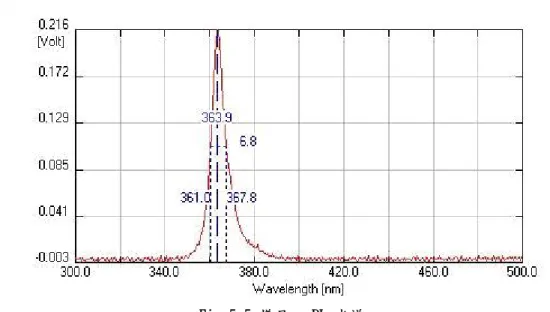
本產學合作計劃第一、二年的目標方面,第一年我們完成了氫化物氣相磊晶系統 (Hydride Vapor Phase Epitaxy, HVPE)的機台架設和測試,並且成功及穩定的產出厚 度 200μm 以上,直徑分別為 1 吋以及 1.5 吋的氮化鎵厚膜。在第二年的研究中,利用自 行新開發出的 temperature ramping 磊晶方法,將厚膜的直徑成功增加到 1.8 吋與 2 吋, 並將此方法申請專利。並且我們也利用 Nd:YAG 雷射,建構了雷射剝離系統(Laser Lift-Off, LLO),可以將 HVPE 製作的氮化鎵厚膜從原生的藍寶石基板剝離下來,成為 free standing 的氮化鎵基板。我們還利用 regrowth 的方式,將厚膜的的厚度再增加,厚度可 以達到 420μm,此後度足以成為良好之基板。利用 HVPE 和 LLO 系統,成功製作出氮化鎵 基板供後續磊晶元件使用。在氮化鎵晶體的品 質方面,我們利用 X-光繞射(X-Ray Diffraction,XRD)、光致螢光(Photoluminescence,PL)來量測晶體的品質及特性,其 ( 002 ) 面 Rocking Curve 半 高 寬 ( Full Width of Half Maximum , FWHM ) 在 未 和 Sapphire 分離前約 350 arcsec,分離後降低到僅有 150 arcsec,光致螢光的譜線在室溫 時 是 在 364 nm 位 置 , FWHM 大 約 是 6 nm 。 在 電 性 方 面 我 們 利 用 霍 爾 量 測 ( Hall measurement)來計算氮化鎵晶體的載子濃度、載子遷移率,以及電阻值,我們所成長的 氮化鎵晶體,其自然特性為 n-type,載子濃度為 4.9x10¹⁷
/cm3,載子遷移率為 300/V-s, 在缺陷密度方面,我們利用陰極射線發光(Cathodluminescence,CL)映射圖以及蝕刻缺 陷 法 ( Etch Pit Density , EPD ) 來 計 算 晶 體 的 缺 陷 密 度 , 其 ( Threading Dislocations,TDs)大約是介於 106
~~107
/cm2
。在後續製程方面,經過 CMP 的粗磨、中 磨及拋光之後處理,表面的 RMS 降低至 1nm 左右,成為可以成長光電元件之 GaN 基板。
二、
Abstract
The first year, we setup and test the Hydride Vapor Phase Epitaxiy (HVPE) system,
and we made the GaN substrate successfully. The GaN thick‐film with the thickness more than 300 μm and 1 and 1.5 inch diameters were grown by the mentioned above HVPE system. The second year, we use temperament ramping technique to expitaxy GaN substrate and the diameter of GaN substrate is 1.8 and 2 inch. We also use Nd:YAG laser to setup the(Laser Lift‐Off, LLO),which can lift off the GaN thickness from sapphire to form the freestanding GaN substrate. We use the regrowth mention to make the GaN thickness more thicker up to 420 μm, which can be used good substrate. Combine the HVPE and LLO techniques, free‐standing GaN thick‐film were separated from original sapphire substrate. The X‐Ray Diffraction (XRD) and Photoluminescence (PL) measurements were used to check the quality of these thick‐films. The Full Width
of Half Maximum (FWHM) of XRD rocking curve of (002) GaN is about 350 arcsec
before lift‐off from sapphire substrate. The peak position of GaN thick‐film of PL system is 364 nm, and the FWHM of PL peak is 10 nm, showed the quality of free‐standing GaN thick‐film is good. The electronic properties of carrier concentration and mobility of GaN thick‐film were measured by Hall measurement. The GaN thick‐film were grown with naturally n‐type doped. The carrier concentration and mobility were 4.9x10¹⁷/cm3 and 300/V‐s, respectively. The dislocation density was calculated by Cathodluminescence (CL) image and Etch Pit Density (EPD), it showed that, the dislocation density was in the order of 106 to 107 /cm2. After the CMP process, the RMS of roughness is about 1nm, which can be used for the optical device.
三、前言
因為缺乏晶格匹配的同質性基板,現在大多數的三族氮化物(AlGaN、InGaN、 AlInGaN)磊晶都是異質磊晶,利用不同的晶格常數的材料當基板,就像是藍寶石基板上 長氮化物,這時就會有缺陷密度過高,以及散熱不良的問題,此外如果磊晶層較厚,也會 有因為熱膨脹係數不同造成晶體彎曲甚至破裂的問題。在低電流密度的元件中,如 LED 對 於這些缺點都不敏感,若是成長藍光 LD、高功率元件或 UV 元件,類似這種高密度電流元 件,影響就相當可觀。若要解決這些大電流或高功率元件散熱的問題,就必須在晶圓接合 (wafer bonding)、覆晶結構(flip-chip)以及雷射剝離技術上做些努力,但是成本就 勢必大幅增加,而複雜的製程結構也是導致良率下降的主因。若是有單晶的氮化鎵基板, 來進行同質磊晶,不但可以降低晶格常數不匹配所造成的缺陷密度,提昇內部量子效率、 解決熱膨脹係數不同所造成的彎曲;更可大幅簡化元件的製程及提昇元件的可靠度。對未 來在光電元件產業的發展上,單晶氮化鎵基板具有舉足輕重的地位。對於國內學術界而 言,若有單晶三族氮化物基板(GaN、AlN 等)作為研究基礎,在相關領域的研究上等於 直接躍遷至不同的競爭平台上。 台灣在光電半導體的產值及產量方面在世界上都有舉足輕重的地位,然而在國 內對於氮化鎵基板的研發進度卻是相當緩慢,前幾年有持續投入人力在進行研究的只有工 研院電光所及本團隊(交大電物),近年才有中山大學及中央大學以及交大光電相繼投入 HVPE 厚膜技術的開發。本團隊在國內進入 HVPE 厚膜磊晶的起步甚早,目前已具備厚膜的 成長、剝離以及分析的技術,相信在氮化鎵基板的開發可以增進國內光電產業的競爭力, 更可幫助國家厚植實力、培養人材。四、研究背景及目的
1. 三族氮化物光電半導體的發展與應用
2. HVPE 製作基板簡介
3. Laser Lift-off 原理
1. 三族氮化物光電半導體的發展與應用 三族氮化物半導體材料 (InN,GaN,AlN) 他們的二元和三元以及四元化合物都 是屬於直接能隙的材料 (Direct Band Gap),發光效率較高,並且他們的能隙所涵蓋的範 圍很大,從紅外光到紫外光都包含在內,因此受到矚目,被視為相當具有前景的材料,也 持續的被研究。三族氮化物半導體材料中,GaN 具有 3.4eV 的能隙,這是屬於紫外光的波段,若 加入不同的材料如銦 (In),就可以調變波段至藍綠光,這樣可以被應用在藍綠光波段的 發光或是吸光元件,可應用在藍光的發光二極體 (Light Emitting Diode,LED),雷射元 件 (Laser Diode,LD),光檢測器 (Photo Detector) 等等。若是加入鋁 (Al),則波長 變為深紫外光的波段,這在照明和醫療方面都有很廣泛的用途。此外在電性方面,GaN 材 料具有高崩潰電壓與飽和電流的特性,所以具有高電子傳輸速度和低雜訊,並且能夠在高 溫之下操作,也被視為一大用途。
Fig 3.1 是過去 LED 發光效率發展趨勢圖。1960 年代紅光的 LED 已經持續且穩 定的發展,1990 年代藍綠光 LED 才迅速的發展起來,這是因為一直找不到適當的基板。 因為 GaAs、GaP 等基板可以使用在紅光 LED,因此基板的選擇就已經克服,只要在元件結 構上做改善以達到增加發光效率等性能。
理論上藍綠光 LED 有幾種半導體化合物可以使用,一是由 ZnSe、MgS 所構成的 II-VI 族半導體系統,二為 SiC,最後則是三族氮化物所組成的半導體系統,如 Fig 2.2 所 示。不過在 II-VI 族半導體有一缺點便是材料特性不穩定,所以沒有發展的很好,另外 iC 則是沒有搭配的材料可以形成異質結構,又是一個非直接能隙的材料,所以效果更 差。而在三族氮化物半導體中,因為氮的揮發性太高,不能像 GaAs、InP、SiC 等化合物 半導體直接由液相拉晶的方式成長大尺寸的塊材及量產基板,必須在非常大的壓力下才能 形成基板,並且產出的樣品也不大只作為學術研究之用,無法得到發展。 Fig 3. 2 化合物半導體晶格常數對能隙之關係圖
一直到了 1983 年,日本 Yoshida 在藍寶石基板 (Al2O3) 上成長高溫 AlN 緩衝層,發
現在其上成長的 GaN 結晶較好。之後,名古屋大學 I. Akasaki 教授採用低溫 AlN 緩衝層 隨後再採用高溫 (~1000℃)成長 GaN,得到像鏡面一樣的材料。而 1991 年日亞公司 (Nichia) 研究員 S. Nakamura 採用低溫 GaN 緩衝層,再升到高溫成長,同樣得到了高品 質的 GaN 之後,藍綠光的元件才有了藍寶石這個基板可以使用,也因此蓬勃發展。至今這 種藍寶石配合緩衝層的成長方式仍然是業界最常使用的。
2. HVPE 製作基板簡介
以 HVPE 技術製作 GaN 及 AlN 基板的流程圖可以下圖來大致說明。
Sapphire subs
HVPE
Sapphire subs
GaN thick film LLO or self-separation
Sapphire subs GaN thick film
GaN thick film Polish
GaN substrate Sapphire subs
HVPE
Sapphire subs
GaN thick film LLO or self-separation
Sapphire subs GaN thick film
GaN thick film Polish GaN substrate Fig 3. 3 HVPE 製作三族氮化鎵基板流程圖 在 HVPE 厚膜成長及厚膜和原生基板的剝離,為其中關鍵性的兩個步驟,而剝離技 術又以雷射剝離(LLO)最為成熟。 HVPE 早先應用在砷化鎵(GaAs)材料的成長,在氮化鎵單晶厚膜的應用上,由於 Ga 與 NH3無法直接形成 GaN,所以主要是利用氯化氫氣體(HCl)與液態鎵金屬(Ga)反應生成 氯化鎵(GaCl),GaCl 再與氨氣(NH3)反應生成氮化鎵,再沈積到基板上。其主要反應 式如下:
2HCl(g) + 2Ga(melt) ⇔ 2GaCl(g) + H2(g) (eq.1)
GaCl(g) + NH3(g) ⇔ GaN(s) + HCl(g) + H2(g) (eq.2)
主要產物是 GaN,磊晶源 (source)是五族的 NH3(g),跟三族的 HCl 與 Ga 形成的
GaCl(g)。HVPE 跟 MOCVD 的成長方式類似,都是由相同的五族 NH3,不同的是三族的磊晶
源 MOCVD 使用的是 TMGa 或者是 TEGa 的有機金屬化合物來做成長。因為五族磊晶源容 易揮發,所以成長的時候的 V/III 比都大於 1。
在 HVPE 成長 GaN 中,擁有極高的成長速率(~100μm/hr),對於成長厚膜相當有利, 並且長晶的品質良好,對於成長獨立式基板是最適合的一種長晶方式,唯一的缺點就是表
Fig 3. 4 HVPE 成長 GaN 原理
3. Laser Lift-off 原理 雷射剝離原理如下圖所示 scanning laser-pulse thermal-decomposition N2 Al2O3 liquid-Ga laser-pulse thermal-decomposition scanning N2 Al2O3 liquid-Ga
Fig 3. 5 Laser lift off 原理
雷射源可以選用 Excimer KrF 或 Q-Switch Nd:YAG pulse laser,以 YAG 雷射為例, 其波長在 1064 nm,經過二倍頻及三倍頻晶體混頻成 355 nm 波長後,利用 Q-Switch pulse 方式激發以達到較大的輸出功率來擊打 GaN/Al2O3介面,由於 Sapphire 對此雷射波
段長並不吸收,使得雷射光會穿透 Sapphire 而到達 GaN/Sapphire 界面,此時界面表層的 GaN 受到雷射高能量開始熱分解形成 N2逸散,因此,GaN 就會和原生基板 Sapphire 分離。
以下將敍述計劃第一、二年的研究方法、步驟。
1. HVPE 系統設計組裝 本實驗室之 HVPE 機台為業界轉移,而在交大復機,HVPE 優點在於成長速度較快,且 品質較好、缺陷密度較小等優點,適合用在製作 GaN 厚膜基板。首先在復機所遇到第一個 部份為氣體流量參數調教的部份,在 HVPE 成長 GaN 基板主要是利用氯化氫氣體(HCl) 與液態鎵金屬(Ga)反應生成氯化鎵(GaCl),GaCl 再與氨氣(NH3)反應生成氮化鎵, 再沈積到基板上,因此在各氣體的流量控制造成三五的變化上將會影響結果甚鉅。第二個 為成長壓力的問題,因為不同壓力和溫度成長時,會造成 GaN 的成長方式是 2D 或是 3D。 還有在成長溫度方面也必須考慮進去,因為低溫成長(約 950℃)和高溫成長(約 1050℃)也 是會影響到長晶的品質。此外,carrier 氣體的使用,也是一項重要的因素,我們選擇了 兩種不同的氣體當作 carrier 氣體,一種為氫氣,一種為氮氣,兩種不同的氣體也會對於 成長的速率或是成長出來品質會有影響。因此在機台的參數條件上面,有許多的變因需要 一一的去嘗試。 2. 雷射剝離系統設計組裝 雷射剝離系統是一項非常值得研究的方向,其用途除了可以用來分離 GaN semi-bulk 和其原生基板外,在現今的藍光 LD 及 LED 製程中也是一項具有前瞻性的技術,因現今藍 光的 LED 製程均是使用 Sapphire 基板來進行異質結構磊晶,而 Sapphire 基板導電性和散 熱效果都很差,使得藍光及白光 LED 的發光效益不好,並且無法製做背面電極來增加散熱 效果以及有效發光面積,如果可以使用雷射剝離的技術,將在 Sapphire 基板上成長之 GaN LED 結合 Wafer Bonding 的技術轉移到 GaAs 晶片、Si 晶片或銅(Cu)基板上,其散 熱性及 LED 結構都可獲得良好的改善。目前市面上雖然已有商業化 prototype 雷射剝離機 台,但是造價昂貴,而且未經充分驗證,本團隊已有成功設計組裝及使用雷射剝離系統之 經驗而且造價僅為市售機台價格的 1/4。故本計劃第一年的首要項目就是組裝 Laser lift-off 系統,並利用此系統進行獨立式 GaN 及其他三族氮化物基板之開發研究。 Fig4.1 本實驗自行組裝之雷射剝離系統3. GaN 塊材成長技術研究
計劃中我們使用 HVPE 磊晶法來成長 GaN 厚膜
現今以 HVPE 成長的 GaN 厚膜仍必需使用異質磊晶的方式來成長,首先選擇適合的原 生基板,再於其上成長 GaN 厚膜結構,所以選擇可以降低缺陷密度,並可成長 GaN 至一定 厚度之原生基板來進行磊晶成長研究是一個重要的方向。而在這裡我們利用固定的 c-plane sapphire 藍寶石基板,使用溫度 ramping 的方式,利用漸變溫度改變,將原本的 應力較高的問題,做有效的釋放。
另外,在異質磊晶中,Epitaxial‐Lateral‐Overgrowth (ELOG)是有效且方便減少或降 低降低缺陷密度的一種方法,ELOG 所運用的原理磊晶過程中不同的晶面生長速度不同的 特性,將缺陷密集的集中,且引導到不同的方向,使接下來的長晶過程中缺陷密度可以有 效的降低,這種技術已經運用在 GaN 的藍光雷射當中,是一種非常普遍的製程方式。常 見的 LEO 方式有下列幾種:(a)傳統式 LEO (b)Face Initiated LEO (c)懸吊式成長 (PENDO epitaxy) (d)空橋式側向成長 (Air‐bridge LEO)(e)Facet Assisted LEO 等,其中以 Facet Assisted LEO 具有最佳效果。在 MOCVD 系統中 LEO 的研究已經 有相當長的時間,以及擁有許多的相關資料,本計劃將以 HVPE 機台使用 LEO 磊晶方法 研究 GaN semi‐bulk 成長,並藉由及 EPD 的方式來測量缺陷的密度及使用 TEM 來觀測 晶體內部的缺陷分佈情形,以選擇最佳的 LEO 磊晶方法。
本計劃使用 HVPE 磊晶設備,成長 GaN 厚膜結構並使用雙晶 X 光繞射儀,分析晶體之 晶格結構及成分,並利用 SEM 及 AFM 針對 GaN 之表面型貌進行研究,對於溫度 ramping 成長 GaN 厚膜之成長影響,或是 ELOG 方式以掌握成長高品質 GaN 厚膜之參數。
Fig4.2 ELOG 在光學顯微鏡下之條紋
Fig4.3 ELOG 結構示意圖
Fig4.4 ELOG 結構磊晶初始態之 SEM 圖
4. CMP 系統設計組裝 化學技術研磨技術在現今半導體產業,已經是相當成熟的一樣技術。而在本計劃中, 經過雷射剝離之後的 GaN bulk 會有彎曲的現象,或是表面有不平整的現象,我們必須利 用研磨的方式將表面研磨平整,才能接下來後續成長其他光電元件或是再成長 GaN 厚膜, 成為可用的 GaN 基板。 本實驗室的 CMP 的製作流程,是從研磨顆粒 6μm 先做粗磨,主要是消除刻痕,以及 表面的一些高低起伏較大的地方。皆下來利用膠盤配上 2μm 研磨顆粒做中磨,此步驟為 減小 RMS 的重要步驟。接下來利用顆粒更小的 SiO2做拋光,最後用不同酸鹼溶液,最最後 的 chemical polish 的工作。
六、計劃執行結果與討論
1. 利用 HVPE 成長 GaN layer 分析
2. 利用 temperature reamping 成長 GaN thick film 3. Laser Lift-off 探討
4. GaN 厚膜 Regrowth 探討 5. CMP 探討
6. 成長近紫外光 LED
1. 利用 HVPE 成長 GaN layer 分析
在 HVPE 磊晶成長方面,先使用 MOCVD 在 c-plane Sapphire 上成長厚度 4 mm 的 GaN,再以此為 template 放在 HVPE Reactor 中成長 GaN 厚膜。而在 HVPE 中我們利用兩階 段的成長方式,第一階段使用較低的壓力,因為這樣會使得 GaN 有較大的機會朝向 2-D 方 式生長,表面平整度會較佳,第二階段再以高壓方式成長,使 GaN 有較高的生長速率可以 成長較厚的膜厚。而在成長的過程中,皆為在高溫中中成長,使晶體有較佳的品質。在 V/III 比的條件,比例我們控制在 25~100 之間,視不同階段的需求來進行調整。
Fig 5.1 及 Fig 5.2 為此系列結構 HVPE 成長之後的結果,樣品一是在 2 吋 Sapphire 上成長 1.5 吋 GaN 厚膜,表面呈現鏡面,樣品二厚度較厚,有些許的裂痕,在 XRD 的分析 方面,我們使用 Bede D1 的 XRD 來析晶體的品質,以 HVPE 成長 GaN 而言,XRD 分析的結 果會受到膜厚,彎曲度的影響,以樣品一而言,其(002)的 XRD 半高寬因為受到 bending 的影響,所以半高寬較高,大約是 350 arcsec。在電性方面我們使用 Hall 量測 系統來分析,其特性如表 5.1 所列。
Fig 5.2 樣品二 Fig 5.3 樣品一的(002)XRD
Fig 5.4 樣品一 PL mapping
Table 5.1 GaN 厚膜特性量測結果
Wafer Size 1.5 inch Wafer Thickness 30 m Crystal Orientation (001) c-axis
Crystal Structure Wurtzite Growth Face Ga-Face
FWHM of XRD -sacn 346 (GaN on Sapphire) arcsec Resistivity 0.137 -cm Carrier Type n-Type
Carrier Concentration 4.9 x 1017 cm-3 Mobility 306 cm2/V-s
2. 利用 temperature reamping 成長 GaN thick film
m-1
,換算出來的壓縮 力分別是 0.07、0.12 和 0.12GPa,可發現大幅降低應力之產生。
此外我們利用 ramping 的方式成長厚膜,先利用 MOCVD 成長約 4μmGaN 在 c-plane 的 sapphire 上,再利用 HVPE 成長 950℃的 LT GaN,接下來利用溫度 ramping 的方式從 950℃到 1050℃,上升的速率分別為 3.3、1.7、1.0、0.8℃/min,然後維持 1050℃直到 GaN 厚度達到 300μm,之後利用 LLO 將樣品從 sapphire 上剝離,而得到 1.5 和 2 吋的 GaN 厚膜。利用拉曼量測完全無應力的情況下拉曼光譜偏移量是 567cm-1 ,而在有緩慢升溫 製程的樣品中,其偏移量由上而下分別是 567.3、567.5 和 567.5 c 應
Fig 5.6 利用 HVPE 成長溫度 ramping 結構圖
Fig 5.7(a)利用溫度 的樣品,呈破裂狀
(b) A300 mm crack free freestanding GaN 利用 LLO 技術剝離
Fig 5.8 Cross-sectional CL 的圖片 (a) 3.3 o
C/min. (b) 1.7 o C/min. (c) 1.0 o C/min. (d) 0.8 o C/min.
(a)
(b)
(c)
(d)
(a)
(b)
(a)
(b)
Fig 5.10 (a) rocking curve of HRXRD of the freestanding 的 GaN ramping 速率為 1.0 o
C/min. FWHM 值為 156.7 arcsec。 (b) Top view CL 的 freestanding GaN 基板.黑點為 dislocation 所在,缺陷
密度約為 107
/cm2
。
(a)
(b)
Fig 5.11 (a) 2 吋厚度 300 mm GaN on sapphire substrate 未剝離 (b)經過 LLO 之 Freestanding GaN wafer,右邊為剝離後之 sapphire( Cooperated with ITRI)
3. ELOG 技術探討
在實驗中我們也使用在 GaN template 上做 ELOG 結構來成長 GaN 厚膜,這樣可以減小 dislocation density,並且也可以降低因為 GaN 厚膜和 Sapphire 的晶格不匹配或是熱膨 脹系數不同所造成的應力。我們利用 MOCVD 先成長 4μm 厚的 GaN template,皆下來再使 用黃光製程的方式,在 GaN template 上開出 5:5 (window:mask)到 15:75 不等的比 例,接著送進去 HVPE 坐在成長的步驟,圖 5.12 為 window:mask 為 5:5 ELOG 結構 GaN template 利用 HVPE 成長厚膜之初始態。圖中由上到下是分別成長 5 分鐘、7 分鐘、9 分 鐘的狀況,在成長五分鐘時,GaN 還沒接合,到 9 分鐘時已經在 ELOG 部分都已接合,再 成長更長時間會接平,因此在初始態分鐘成長是一個重要的參考值,再這裡 ELOG 結構在 形 成 三 角 形 結 構 後 , 必 須 改 變 溫 度 以 及 壓 力 讓 三 角 形 結 構 變 為 側 向 的 成 長 , 讓 Dislocation density 降低。在 ELOG 接平之後繼續長到數百微米的厚度,之後再以 Laser Lift-off 技術將 GaN 厚膜自 Sapphire 上剝離。
圖 5.13 為利用 HVPE 在 MOCVD GaN template 上成長約 300μm 的,再利用 LLO 技術自 Sapphire 上剝離的 freestanding GaN 厚膜,圖中央白線是在切割時造成的龜裂,圖 5.14 是其正面的 SEM 照片,由 SEM 照片顯示,其表面沒有明顯的缺陷,局部平整度良好。圖 5.15 為另一塊樣品的表面 CL image,圖中黑點可以代表 dislocation density,其密度 大約是 2.3 x 10⁷
Fig5. 12 ELOG 結構 GaN 厚膜成長隨時間之變化
Fig5.13 Cross section SEM image of freestanding GaN thick-film(李威儀教授實驗室)
Fig5. 14 Plane view SEM image of freestanding GaN thick-film(李威儀教授實驗室)
Fig5. 15 CL image plane view of freestanding GaN thick-film (李威儀教授實驗室)
4. Laser Lift-off 探討 在 Laser Lift-Off 分離厚膜的技術方面,我們也做了許多的嘗試,並且有了不錯的 結果。和使用自我分離技術(self-separation)方法比較,使用 LLO 的方法來離 GaN 厚 膜,在分離之後其彎曲的程度較小,較利於後續 CMP 的製程,我們所使用的系統為 Nd:YAG 355 nm 雷射,對於 GaN 和 Sapphire 的分離而言由於其波長接近 GaN 的能隙,吸 收效率佳,功率也比 KrF 準分子雷射來得小,對 GaN 和 Sapphire 的分離而言所造成 GaN 破碎和熱傷害的影響也較小。我們調變雷射的功率、以及在晶片上掃描的速率、以及雷射 的 beam size 來達到最好的分離效果,如果雷射功率過大或 beam size 過大,容易使 LLO 之 GaN 產生碎裂情形。若因雷射的功率及 beam size 調整過大,易產生碎裂的情形。
Table 5.2 由 LLO 系統剝離之 1.5 inch Freestanding GaN 特性(李威儀教授實驗室)
Fig 5.17 1.8 吋 300um GaN 厚膜及由 LLO 系統剝離之 1.8 inch Freestanding GaN (李威儀教授實驗室)
Fig 5.18 2 吋 300um GaN 厚膜及由 LLO 系統剝離之 2.0 inch Freestanding GaN(李威儀教授實驗室, Cooperated with ITRI)
5. GaN 厚膜 Regrowth 探討
當厚膜長至一定厚度時,因為應力會增大,所以容易碎裂,因此我們利用 regrowth 的方式,繼續的將厚膜的厚度增厚。首先是將成長完的厚膜,利用 LLO 的方式將 GaN 從 sapphire 上剝離,成為 free-standing 的 GaN 基板,再送入 HVPE 繼續成長。這樣有兩種 好處,因為這樣變成是同質磊晶,這樣可以減少缺陷的產生,並且能降低 bowing 的程 度。從 XRD 的數據可以得知,半高寬明顯的減少,在(002)面為 FWHM=120.85 arcsec; (102)面的 FWHM=107.57 arcsec,皆比 free standing 的半高寬小。
Fig 5. 21 Regrowth 後,GaN 的(102)面的 XRD
Fig 5.22 (左)1.5 吋 free standing GaN 基板 (右) 1.5 吋 free standing GaN 基板上 regrowth 1.22 吋的 GaN 厚膜,下方裂痕為原本 free standing GaN 的裂痕延伸上來,厚度從 200μm 增加至 560μm
將 Laser Lift Off 之後的樣品,利用 CMP 的製程技術,將表面粗糙的厚膜,研磨成 表面光滑可成長元件的 GaN 基板。首先我們利用直徑為 6μm 的顆粒先研磨,接下來利用 2μm 的顆粒再中磨,而後再使用 SiO2顆粒細拋。再來進入 CMP,利用 SiO2+C6H8O7+NaOCl 的
溶液,做初步的處理,最後做 FCMP 用 C6H8O7+NaOCl,做最後的研磨。這樣子可以將表面的 RMS 縮小至 1nm 左右,或甚至更小。 Fig 5.23 利用 CMP 研磨完成的 GaN 破片樣品,RMS 為 1.21nm Fig 5.24 利用 CMP 研磨完成的 GaN 破片樣品,RMS 為 0.74nm
我 們 利 用 上 述 的 方 式 , 將 GaN 厚 膜 使 用 LLO 技 術 剝 離 , 再 將 GaN 送 回 HVPE regrowth,使厚度增厚,最後利用 CMP 製程將 GaN 磨平,成為可以成長近紫外光 LED 的 GaN 基板。
我們將此處理過的 GaN 基板利用 MOCVD 成長近紫外光 LED,因為在 CMP 製成過程中, 會造成 damage layer 的產生,我們利用兩種方法來消除 damage layer,一種為使用 H2SO4:H3PO4=1:3 在 220℃中做蝕刻,第二種是使用 RIE 做蝕刻,將 damage layer 去除,接
著成長近紫外光 LED 結構。
而接過兩種表面處理的 GaN 基板所成長的藍光 LED,經過 PL 量測,發光波長大約是 416.5nm、416nm,而 FWHM 兩者分別是 21.8nm 和 16nm,經過 RIE 處理過的半高寬比較 好。而近紫外光 LED 的 turn on voltage 大約是 3.5V 左右。
Fig5.25 (左)為經過 H2SO4:H3PO4=1:3 在 220℃處理過 (右)為經過 RIE 處理 的 GaN 基板所成長近紫外光 LED 之 PL
Fig5.27 經過 RIE 表面處理未做 chip 的近紫外光 LED 的 I-V 特性曲線
Fig5.28 經過 RIE 表面處理 chip 製作完成的近紫外光 LED 的 I-V 特性曲線
七、結論
本 研 究 計 畫 利 用 HVPE 系 統 以 及 自 行 開 發 出 temperature ramping growth technique,來成長 GaN 厚膜已經可以達到 300mm 以上的厚度,並且尺寸已經能夠在 1.5 吋大小穩定的產出,且在 1.8 吋到 2 吋的大小也已經能夠掌握其訣竅,並成功產出,再 則,利用溫度 ramping 的方式,更能在應力釋放和品質上也做到良好的改善。在雷射剝離 技術方面,利用這個技術可以將 1.5 吋到 2 吋的 GaN 厚膜成功的從 sapphire 上剝離。CMP 部分也可以將表面的 RMS 縮小至 1nm 左右,甚至以下。而我們也利用經過 regrowth 和 CMP 的製程所製作的 GaN 基板成長近紫外光 LED,也能順利發光。經過我們這些的努力, 期望能提供 GaN 基板,可以供後續的成長元件使用。
八、發表成果
(一)計畫執行期間發表之論文
a.期刊論文
1. Hsin-Hsiung Huang, Kuei-Ming Chen, Li-Wei Tu, Ting-Li Chu, Pei-Lun Wu, Hung-Wei Yu, Chen-Hao Chiang, and Wei-I Lee, “A Novel Technique to Grow Crack-Free GaN Thick Films by Hydride Vapor Phase Epitaxy”, Jpn. J. Appl. Phys. 47, 8394 (2008) (SCI) NSC 95-2622-E-009-011
2. Hsin-Hsiung Huang, Pei-Lun Wu, Hung-Yu Zeng, Po-Chun Liu, Tung-Wei Chi, Jeng-Dar Tsay, and Wei-I Lee, “Triangular Extended Microtunnels in GaN Prepared by Selective Crystallographic Wet Chemical Etching”, J. Electrochem. Soc. 155, H504 (2008) (SCI) NSC 95–2622-E-009–011
3. Wen-Chien Yu, Shu-Mai Ye, Feng-Ke Hsiao, Chi-Ling Lee, and Wei-I Lee, “Formation of nitride laser cavities with cleaved facets on transferred laser diodes on GaAs substrates”, Phys. Stat. Sol. C5, 2139 (2008) (SCI)
4. Pei-Lun Wu, Hsin-Hsiung Huang, Hung-Yu Zeng, Po-Chun Liu, Chih-Ming Lai , Jeng-Dar Tsay, and Wei-I Lee, “Comparison Between Extended Microtunnels Along Different Crystal Orientations in GaN”, Phys. Stat. Sol. C 5, 1671 (2008) (SCI) NSC 95–2622-E-009– 011
5. Wen-Chien Yu, Shu-Mai Ye, Feng-Ke Hsiao, Chi-Ling Lee, and Wei-I Lee, “Formation of nitride laser cavities with cleaved facets on transferred laser diodes on GaAs substrates”, Phys. Stat. Sol. C5, 2139 (2008) (SCI)
6. Yen-Teng Ho, Mei-Hui Liang, Feng-Ke Hsiao, Wei-Lin Wang, Chun-Yen Peng, Wei-Da Chen, Wei-I Lee, Li Chang, “Non-polar a-plane GaN grown on LaAlO3 (001) substrate by pulsed laser deposition”, J. Crystal Growth 310, 1614 (2008) (SCI)
7. Hsin-Hsiung Huang, Hung-Yu Zeng, and Wei-I Lee, “Preparation of Extended Microtunnels in GaN by Wet Chemical Etching”, Phys. Stat. Sol. B 244, 1872 (2007) (SCI) NSC 95-2112-M-009-001 J. F. Chen, C. T. Ke, P. C. Hsieh, C. H. Chiang, W. I. Lee, and S. C. Lee, “Deep-level Emissions in GaAsN/GaAs Structures Grown by Metal Organic Chemical Vapor Deposition”, J. Appl. Phys. 101, 123515 (2007) (SCI)
8. Chi-Ling Lee and Wei-I Lee, “Effects of Strained InGaN Interlayer on Contact Resistance Between p-GaN and Indium Tin Oxide”, Appl. Phys. Lett. 90, 181125 (2007) (SCI)
9. Chi-Ling Lee and Wei-I Lee, “Using Planarized p-GaN Layer to Reduce Electrostatic Discharge Damage in Nitride-Based Light-Emitting Diode”, Jap. J. Appl. Phys. 46, L457 (2007) (SCI) NSC 95-2112-M-009-001
10. Hsin-Hsiung Huang*, Hung-Yu Zeng, Chi-Ling Lee, Shih-Chang Lee, and Wei-I Lee, “Extended Micro-tunnels in GaN Prepared by Wet Chemical Etch”, Appl. Phys. Lett. 89, 202115 (2006) (SCI) NSC 94-2112-M-009-012
11. Chi-Ling Lee*, Shih-Chang Lee, and Wei-I Lee, “Nonlithographic Random Masking and Regrowth of GaN Microhillocks to Improve Light-Emitting Diode Efficiency”, Jpn. J. Appl. Phys. 45, L4 (2006) (SCI) NSC 93-2112-M-009-030
b.研討會論文
1. Kuei-Ming Chen, Hsin-Hsiung Huang, Chen-Hao Chiang, Pei-Lun Wu, Ting-Li Chu, Hung-Wei Yu, and Hung-Wei-I Lee ,“Freestanding GaN by hydride vapor-phase epitaxy using template weakness with laser assistance technique”, International Workshop on Nitride semiconductors (IWN2008), Montreux, Switzerland 2008
2. Hsin-Hsiung Huang, Chu-Li Chao, Tung-Wei Chi, Yu-Lin Chang, Po-Chun Liu, Li-Wei Tu, Jenq-Dar Tsay, Hao-Chung Kuo, and Wei-I Lee, “Strain reduced GaN thickfilm grown by Hydride Vapor Phase Epitaxy utilizing dot air-bridged structure”, International Workshop on Nitride semiconductors (IWN2008), Montreux, Switzerland 2008
3. Hsin-Hsiung Huanga,, Chen-Hao Chianga, Kuei-Ming Chena, Ting-Li Chua, Pei-Lun Wua, Hung-Wei Yua, Wei-I Leea, and Li-Wei Tub, “Crack free free-standing bulk GaN grown by Hydride Vapor Phase Epitaxy” International Symposium on Growth of III-Nitrides (ISGN 2008), Laforet Shuzenji, Izu, Japan
4. Kuei-Ming Chen*, Hsin-Hsiung Huang, Feng-Ke Hsiao,Yi-Lin Kuo, Pei-Lun Wu, Ting-Li Chu, Hung-Wei Yu, and Wei-I Lee, “The bowing reduction of Freestanding GaN by N-face regrowth with hydride vapor-phase epitaxy” International Symposium on Growth of III-Nitrides (ISGN 2008), Laforet Shuzenji, Izu, Japan
5. Hsin-Hsiung Huang, Kuei-Ming Chen , Pei-Lun Wu, Hung-way Yu, Ting-Li Chu, Po-Chun Liu, Jenq-Dar Tsay and Wei-I Lee, “Freestanding GaN grown by Hydride Vapor Phase Epitaxiy”, The 2008 annual meeting of the physics society of republic of china (PSROC2008), Hsin-chu, Taiwan, 2008
6. Ting-Li Chu , Hsin-Hsiung Huang, Po-Chun Liu, Tung-Wei Chi, Jenq-Dar Tsay , Kuei-Ming Chen, Pei-Lun Wu, and Wei-I Lee,” The study of chemical wet etching on a-plane GaN thin film”, The 2008 annual meeting of the physics society of republic of china (PSROC2008), Hsin-chu, Taiwan, 2008
7. Kuei-Ming Chen, Hsin-Hsiung Huang, Chen-Hao Chiang, Yen-Hsien Yeh, Yin-Hao Wu, Ting-Li Chu, Din-Ru Yang, Kai-Shiang Liu, Jun-Wei Chen, Zhong-Shan Gao, Wei-I Lee, “Effective Technique for Growing Crack-Free GaN Thick Film by Hydride Vapor Phase Epitaxy”, International conference on Optics and Photonics Taiwan (OPT2008), Taipei, Taiwan, 2008
8. Hsin-Hsiung Huang, Po-Chun Liu, Tung-Wei Chi, Ming-Zheng Hsu, Yu-Lin Chang, Li-Wei Tu, Jenq-Dar Tsay, and Wei-I Lee ,”Improvement of GaN Quality Prepared by Hydride Vapor Phase Epitaxy Using Air-Bridged Growth Technique”, International Conference of Nitride Semiconductors (ICNS-7) Conference, Las Vegas,USA, 2007
9. Hsin-Hsiung Huang, Pei-Lun Wu, Hung-Yu Zeng, Feng-Ke Hsiao, Po-Chun Liu, Tung-Wei Chi, Jenq-Dar Tsay, and Wei-I Lee ,”Comparison Between Extended Microtunnels Along Different Crystal Orientations in GaN”,International Conference of Nitride Semiconductors (ICNS-7) Conference, Las Vegas,USA, 2007
10. Wen-Chien Yu, Shu-Mei Ye, Feng-Ke Hsiao, Chi-Ling, and Wei-I Lee, ”Formation of Nitride Laser Cavities with Cleaved Facets on Transferred Laser Diode on GaAs substrates”, 7th International Conference on Nitride Semiconductors, USA, Las Vegas (2007)
(二)專利
1. Wei-I Lee, Hsin-Hsiung Huang, and Hung-Yu Zeng, “ Etching Method for Nitride Semiconductor”, in requestion of ROC and USA patents, S96005_US1
2. Wei-I Lee, Hsin-Hsiung Huang, Kuei –Ming Chen, and Yen-Hsien, Yeh,” A Novel Technique to Grow GaN Thick-Film by Hydride Vapor Phase Epitaxy”, in requestion of ROC, PRC, and USA patents ,NCTU 提案編號:08(專)A110
九、參考文獻
1. H.M Kim et al. “Preparation of large area free‐standing GaN substrate by HVPE using mechanical polishing liftoff method” Material letters 47(2001) pp.276~280 2. R.J. Molnar et al. “Growth of gallium nitride by hydride vapor‐phase epitaxy” Journal of Crystal Growth 178, pp.147~156(1997 3. Kazumasa Hiramatsu at el. “Fabrication and characterization of low defect density GaN using facet‐controlled epitaxial overgowth (FAELO)” , Journal of Crystal Growth, 221 pp. 316~326 (2000) 4. J. I. Pankove, “Gallium Nitride (GaN) I”(Academic press, San Diego, 1998) 5. X. Xu et al. “Growth and characterization of low defect GaN by hydride vapor phase epitaxy” Journal of Crystal Growth 246 pp223–229 (2002) 6. L. Zhang et al. “Lateral epitaxial overgrowth of GaN using diethyl gallium chloride in metal organic vapor phase epitaxy” Journal of Crystal Growth 235 pp115–123 (2002) 7. S. Gu et al. “The impact of initial growth and substrate nitridation on thick GaN growth on sapphire by HVPE” Journal of Crystal Growth 231 pp342– 351 (2001) 8. Wang et al. “Influences of mask width, fill factor, HCl addition and C doping on wing tilts in the epitaxial laterally overgrown GaN films by HVPE” Appl. Phys. Lett., Vol. 80, No. 25, 24 June 2002 9. X. Xu et al. “Growth and characterization of low defect GaN by hydride vapor phase epitaxy” Journal of Crystal Growth 246 (2002) 223–229 10. X. Xu et al. “Fabrication of GaN wafers for electronic and optoelectronic devices” Optical Materials 23 (2003) 1–5 11. Michal K. KELLY et al. ”Large Free‐Standing GaN Substrates by Hydride Vapor Phase Epitaxy and Laser‐Lnduced Liftoff” , Japan Journal of
substrates and GaN layers grown by different techniques” Journal of Crystal Growth 257 (2003) 1–6 14. C. Wang et al. “Influence of growth parameters on crack density in thick epitaxially lateral overgrown GaN layers by hydride vapor phase epitaxy” Journal of Crystal Growth 230 (2001) 377–380 15. J.‐w. Lee et al. “Low temperature buffer growth to improve hydride vapor phase epitaxy of GaN” Materials Science and Engineering B59 (1999) 12–15 16. H. Jin Kim et al. “Pre‐treatment of low temperature GaN buffer layer deposited on AlN/Si substrate by hydride vapor phase epitaxy” Surface and Coatings Technology 131 (2000) pp465‐469 17. H.M. Kim et al. “Comparison of HVPE GaN films and substrates grown on sapphire and on MOCVD GaN epi‐layer” Materials Letters 46 (2000) pp286– 290 18. H.M. Kim et al. “Preparation of large area free‐standing GaN substrates by HVPE using mechanical polishing liftoff method” Materials Letters 47 (2001) pp276–280 19. W. Zhang et al. “Modulated growth of thick GaN with hydride vapor phase epitaxy” Journal of Crystal Growth 234 (2002) pp616–622 20. Zhang et al. “Dislocation reduction in GaN grown by hydride vapor phase epitaxy via growth interruption modulation” Appl. Phys. Lett., Vol. 78, No. 6, 5 February 2001 21. W. Gotz et al. “Electronic and structural properties of GaN grown by hydride vapor phase epitaxy” Appl. Phys. Lett. 69 (2), 8 July 1996 22. Gotz et al. “Hall‐effect analysis of GaN films grown by hydride vapor phase epitaxy” Appl. Phys. Lett., Vol. 72, No. 10, 9 March 1998 23. Goss et al. “Microcathodoluminescence of impurity doping at gallium nitride/sapphire interfaces” Appl. Phys. Lett., Vol. 78, No. 23, 4 June 2001 24. Oh et al. “Optical properties of GaN grown by hydride vapor‐phase epitaxy” Appl. Phys. Lett., Vol. 78, No. 3, 15 January 2001 25. Sung S. PARK et al.“Free‐standing GaN Substrates by Hydride Vapor Phase Epitaxy” , Japan Journal of Applied Physics Vol.39 pp. L1141~L1142 (2000) 26. F. Yun et al. “Electrical, structural, and optical characterization of freestanding GaN template grown by hydride vapor phase epitaxy” Solid‐ State Electronics 44 pp2225‐2232 (2000) 27. J.A. Freitas Jr. et al. “Structural and optical properties of thick freestanding
GaN templates” Journal of Crystal Growth 231 pp322–328 (2001) 28. Oila et al. “Ga vacancies as dominant intrinsic acceptors in GaN grown by hydride vapor phase epitaxy” Appl. Phys. Lett., Vol. 82, No. 20, 19 May 2003 29. Jasinski et al. “Characterization of free‐standing hydride vapor phase epitaxy GaN” Appl. Phys. Lett., Vol. 78, No. 16,pp2297~2299(2001) 30. M. Bockowski et al. “Directional crystallization of GaN on high‐pressure solution grown substrates by growth from solution and HVPE” Journal of Crystal Growth 246 (2002) 194–206 31. P.R. Hageman et al. “Thick GaN layers grown by hydride vapor‐phase epitaxy/hetero‐ versus homo‐epitaxy” Journal of Crystal Growth 255 (2003) 241–249 32. A. Trassoudaine et al. “Temperature influence on the growth of gallium nitride by HVPE in a mixed H2/N2 carrier gas” Journal of Crystal Growth 260 (2004) 7–12 33. I. Nikitina et al. “Dislocation structure of GaN bulk crystals grown on SiC substrates by HVPE” Materials Science and Engineering B 61–62 (1999) 325– 329 34. J. Chaudhuri et al. “High quality GaN layers grown by hydride vapor phase epitaxy — a high resolution X‐ray diffractometry and synchrotron X‐ray topography study” Materials Science and Engineering B 78 (2000) 22–27 35. G. Nataf et al. “High quality ELO‐GaN layers on GaN.Al2O3 patterned substrates by halide vapour phase epitaxy” Materials Science and Engineering B 59 (1999) 112–116 36. M. Leroux et al. “Luminescence and reflectivity studies of undoped, n‐ and p‐doped GaN on (0001) sapphire” Materials Science and Engineering B 50 (1997) 97–104 37. P. Gibart et al. ” Spatially resolved photoluminescence of laterally overgrown GaN” Journal of Crystal Growth 201/202 (1999) pp365‐370 38. Tavernier et al. ” Two‐step growth of high‐quality GaN by hydride vapor‐ phase epitaxy” Appl. Phys. Lett., Vol. 77, No. 12, 18 September 2000
83, No. 4, 28 July 2003 41. Detchprohm et al. “Hydride vapor phase epitaxial growth of a high quality GaN film using a ZnO buffer layer” Appl. Phys. Lett., Vol. 61, No. 22, 30 November 1992 42. H. Sone et al. “Optical and Crystalline Properties of Epitaxial‐Lateral‐ Overgrown‐GaN Using Tungsten Mask by Hydride Vapor Phase Epitaxy” Jpn. J. Appl. Phys., Vol.38, pp.L356~L359 (1999) 43. Yoshiaki Honda et al.”Crystal Orientation Fluctuation of Epitaxial‐Lateral‐ Overgrown GaN with W Mask Observed by Transmission Electron Diffraction and X‐Ray Rocking curves” , Japan Journal of Applied Physics Vol.38 pp. L1299~L1302 (1999) 44. H. Miyake et al. “Carrier‐gas dependence of ELO GaN grown by hydride VPE” Journal of Crystal Growth 237–239 (2002) 1055–1059 45. K. Motoki et al. “Preparation of Large Freestanding GaN Substartes by Hydride Vapor Phase Epitaxy Using GaAs as a Starting Substrate” Jpn. J. Appl. Phys. Vol. 40 pp. L140–L143 (2001) 46. Y. OSHIMA et al. “Preparation of Freestanding GaN Wafers by Hydride Vapor Phase Epitaxy with Void‐Assisted Separation” Jpn. J. Appl. Phys. Vol. 42 (2003) Pt. 2, No. 1A/B 47. Li, Bishop, and Coleman, “GaN epitaxial lateral overgrowth and optical characterization”, Appl. Phys. Lett., Vol. 73, No. 9,pp1179~1181(1998) 48. 趙偉清 “氫化物氣相磊晶法成長單晶氮化鎵" 國立交通大學電子物理所論 文,2002 49. Claudio R. Misky, et al. “Freestanding GaN‐substrate and devices”,phys. stat. sol. (c) 0, No. 6 (2003) 50. D. F. Storm, et al “Growth and characterization of plasma‐assisted molecular beam epitaxial‐grown AlGaN/GaN heterostructures on free‐ standing hydride vapor phase epitaxy GaN substrates”, J. Vac. Sci. Technol. B 23.3., May/Jun 2005 51. A.E. Nikolaev, et al. “GaN Layers Grown by HVPE on P‐type 6H‐SiC Substrates”, N. S. R. Vol 1, Art 45 52. 郭怡麟 “獨立式氮化鎵基板之研發" 國立交通大學電子物理所論文,2005