Improved Stability/Variability for Ultralow Voltage
Near Subthreshold Operation
Vita Pi-Ho Hu, Member, IEEE, Ming-Long Fan, Student Member, IEEE, Pin Su, Member, IEEE,
and Ching-Te Chuang, Fellow, IEEE
Abstract—This paper analyzes and compares the stability,
mar-gin, performance, and variability of ultrathin-body (UTB) SOI 6T
SRAM cells operating near the subthreshold region with different
threshold voltage (V
t h) design. Our results indicate that UTB SOI
6T SRAM cell using low V
t hdevices (
|V
t h| = 0.19 V) shows a
com-parable read static noise margin (RSNM), 41% improvement in
σRSNM, 84% improvement in write static noise margin (WSNM),
and 67% improvement in σWSNM as comparaed with the case
using higher V
t hdevices (
|V
t h| = 0.49 V). As V
t hdecreases (work
function moves to the band edge), the “cell” access time improves
significantly with correspondingly higher standby leakage. For low
V
t hdevices (|V
t h| = 0.19 V), it is shown that lowering bit-line
precharge voltage by 50 mV reduces the standby leakage by 20%.
Our study suggests that the lower V
t hdevices operating slightly
into super-threshold region improve the stability/variability
signif-icantly and offer higher performance for ultralow voltage SRAM
applications.
Index Terms—Metal gate, SOI, subthreshold SRAM,
ultrathin-body, variability.
I. I
NTRODUCTIONS
UBTHRESHOLD operation is an efficient technique to
achieve ultralow power consumption for circuits by
lower-ing the power supply (V
dd) below the threshold voltage (V
th)
[1], [2]. UTB SOI MOSFET with thin buried Oxide (BOX)
has emerged as a promising candidate to extend CMOS
scal-ing [3]–[5]. Due to its better control of short-channel effects,
lower subthreshold swing, and reduced leakage and random
dopant fluctuation (RDF) resulting from the use of undoped
(or lightly doped) thin silicon film, UTB SOI MOSFET is very
attractive for subthreshold circuit applications.
Metal-gates and high-k dielectrics are key performance
boost-ers for CMOS technology in the sub-45 nm nodes. Work
func-Manuscript received May 25, 2010; accepted December 28, 2010. Date of publication May 2, 2011; date of current version July 3, 2013. This work was supported in part by the National Science Council of Taiwan under Contract NSC 99–2221-E-009–174, in part by the Ministry of Education in Taiwan under the Aiming for the Top University Program, and in part by the Ministry of Economic Affairs in Taiwan under Contract 99-EC-17-A-01-S1–124. The review of this paper was arranged by Associate Editor B. Yu.
The authors are with the Department of Electronics Engineering, and Institute of Electronics, National Chiao Tung University, Hsinchu 30010, Taiwan (e-mail: [email protected]; [email protected]).
Color versions of one or more of the figures in this paper are available online at http://ieeexplore.ieee.org.
Digital Object Identifier 10.1109/TNANO.2011.2105278
tion engineering for metal-gates devices has been intensively
re-searched to obtain adequate/low threshold voltages for high
per-formance CMOS devices [6]–[11]. The use of a single midgap
metal-gate such as TiN on SOI MOSFET provides suitable
threshold voltage for n-channel and p-channel devices
simul-taneously while keeping the channel undoped [9]. Single-metal
single-dielectric (SMSD) engineering remains the simplest and
most cost effective of many techniques proposed to achieve
the need for multi-V
thdevices [10]–[12]. UTB SOI SRAM
cells with midgap work function devices (
|V
th|
∼0.49 V, V
dd=
0.4 V) operating in the subthreshold region show sufficient
mar-gin [13]–[15]. However, the impact of threshold voltage design
on the stability, performance, and variability of UTB SOI SRAM
for ultralow voltage near subthreshold operation has rarely been
examined.
In this paper, we analyze and compare the stability, margin,
performance, and variability of UTB SOI 6T SRAM cells with
lower and higher V
thdevices. We assess the feasibility of using
lower V
thdevices for ultralow voltage near subthreshold SRAM
design. The lower V
thdevices (with quarter band gap work
func-tion) are shown to be capable of supporting the high performance
applications, and improving the stability/variability and offering
higher performance while trading off leakage for the ultralow
voltage SRAM applications. This paper is organized as follows.
Section II describes the device design and characteristics used
in this study. Section III investigates the impact of V
thdesign on
the UTB SOI SRAM cells for ultralow voltage near subthreshold
operation, including RSNM, WSNM, “cell” read access time,
time-to-write, and cell leakage. Section IV evaluates the
effec-tiveness of commonly used circuit techniques, such as word-line
voltage lowering, bit-line precharge voltage lowering, and
nega-tive bit-line voltage, for improving the stability, standby leakage,
and write ability of the UTB SOI SRAM cell for ultralow voltage
near subthreshold opeartion with lower V
thdevices. Section V
compares the variability (σRSNM, σWSNM) of the 6T UTB
SOI SRAM cells with low and high V
thdevices. Section VI
concludes the paper.
II. D
EVICED
ESIGN ANDC
HARACTERISTICSIn the following sections, we investigate the cell stability,
performance, leakage, and variability of UTB SOI 6T SRAM
cells with channel doping concentration = 1e16 cm
−3, BOX
thickness = 10 nm, gate length = 40 nm, EOT = 1 nm, and
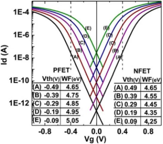
Fig. 1. Log(Id)–Vg characteristics for UTB SOI MOSFETs with various threshold voltages (Vth)/work functions (WF) at Vd = 0.4 V. The |Vth| of NFET and PFET in each case (A–E) are designed with the same absolute value.
(Vg = Vth @ Id = 3e–7 A).
channel thickness = 10 nm. The mobility ratio of NFET to PFET
is around 2.5. TCAD mixed-mode device/circuit simulations
[16] are employed to analyze the performance of UTB SOI
SRAM cells. Fig. 1 shows the log(Id)–Vg characteristics of five
cases analyzed in this study. Case (A) uses midgap work function
for N/PFET and shows higher V
th(
|V
th| = 0.49 V). Case (B),
(C), (D), and (E) employ dual work functions for N/PFETs and
show
|V
th| = 0.39, 0.29, 0.19, 0.09 V, respectively. For each case
in Fig. 1, the absolute value of threshold voltages for NFET and
PFET are the same. From case (A) to (E), the work function
moves successively to the bandedge, and hence successively
lower threshold voltage for the devices.
III. UTB SOI SRAM C
ELLS FORU
LTRALOWV
OLTAGEN
EARS
UBTHRESHOLDO
PERATIONA. Read Static Noise Margin
Fig. 2 shows the read static noise margin (RSNM) comparison
between higher V
th(case A) and lower V
th(case B, C, D,
and E) UTB SOI SRAM cells at V
dd= 0.4 V. The inset of
Fig. 2(a) shows the schematic of a 6T SRAM cell. The inset
of Fig. 2(b) illustrates the static voltage transfer characteristics
(VTC) during read/write operations. The RSNM is defined as the
minimum noise voltage present at each of the cell storage nodes
necessary to flip the state of the cell. V
read,0is the read disturb
voltage determined by the voltage divider effect between
pass-gate and pull-down transistors (NR). V
tripis the voltage needed
to flip the cell inverter. V
gainis defined as the voltage when the
slope of static VTC equals
−1. Increase in V
read,0, decrease in
V
trip, or decrease in V
gainwill degrade the RSNM. V
w rite,0is
determined by the voltage divider effect between pull-up PFET
and pass-gate transistors. Lower V
w rite,0will benefit the write
static noise margin (WSNM).
Fig. 2(a) shows that cases (A), (B), and (C) have comparable
RSNM. Although the threshold voltages of cases (A), (B), and
(C) are different, the threshold voltages of NFET and PFET
in each case are balanced. Devices in cases (A), (B), and (C)
Fig. 2. Read static noise margin comparison between (a) case A, B, and C, (b) case A, D, and E. The inset of Fig. 2(b) shows the definition of RSNM, WSNM, Vre a d , 0, Vt r ip, Vg a in, Vw rit e , 0.
with relatively higher threshold voltage are operating mostly in
the subthreshold region through the switching period at V
dd=
0.4 V. Fig. 2(b) shows that the V
read,0increases slightly in case
(D) compared with case (A). V
read,0occurs with the V
gsof NR
equals 0.4 V and the V
gsof pass-gate transistor equals (0.4
V-V
read,0). Case (D) with quarter bandgap work functions has
lower threshold voltage (
|V
th| = 0.19 V), the NR and pass-gate
transistor operate in the super-threshold region at V
gs= 0.4 V.
The current (strength) ratio of the NR to the pass-gate transistor
is thus lower in case (D) than in case (A), resulting in higher
Vread,0. Fig. 2(b) also shows the V
gainis lower in case (E) than
in case (A). V
gaincan be seen to occur around VL = 0.17 V,
where V
gsof NR equals 0.17 V and the V
gsof pull-up transistor
(PR) equals
−0.23 V. PFET in case (E) with near band-edge
work function (lower threshold voltage = 0.09 V) operates in
super-threshold region at V
gs=
−0.23 V. Hence, the current
(strength) ratio of the PR to the NR is lower in case (E) than in
case (A). Thus, V
gaindecreases in case (E), squeezing RSNM.
The V
tripis almost the same for all cases.
Fig. 3 shows the V
gain, V
trip, and V
read,0comparison at V
dd= 0.4 V. As the NFET moves into the super-threshold region,
V
read,0increases; as the PFET moves into super-threshold
re-gion, V
gaindecreases. Fig. 4 shows the RSNM comparison with
various V
dd. At V
dd= 0.4 V, transistors with V
th∼ 0.09 V (case
Fig. 3. Vg a in, Vt r ip, and Vre a d , 0comparison of UTB SOI 6T SRAM cells
using different threshold voltage designs.
Fig. 4. RSNM comparison between UTB SOI 6T UTB SRAM cells using different threshold voltage designs with Vdd = 0.2, 0.3, 0.4 V.
case (E) shows 35% decrease in RSNM as compared with case
(A). At V
dd= 0.2 V, the RSNM difference between cases (A)
and (E) is reduced because transistors operate mostly in the
sub-threshold region. Case (D) with
|V
th| = 0.19 V (quarter band
gap work functions) shows comparable RSNM to case (A) with
|V
th| = 0.49 V (single midgap work function).
B. Write Static Noise Margin
V
w rite,0(VL) occurs when the V
gsof pass-gate transistor
(AL) is equal to 0.4 V (VBLB = 0 V, V
R= 0 V) and the V
gsof
PL is equal to
−0.4 V. The inset of Fig. 5 shows the log(Id)–Vd
characteristics for N/PFET UTB SOI MOSFET with various
threshold votlages. With balanced N/PFET (
|V
th| the same for
N/PFET), NFET is stronger than PFET in the super-threshold
region as compared with that in the subthreshold region (see
Fig. 5 inset). This is because compared with (V
gs− V
th), the
contribution of mobility to drain current is more significant
in the super-threshold region than in the subthreshold region.
V
gs− V
thcontributes to current in the exponential term which
influences the subthreshold current more significantly than
mo-bility. The lower mobility in PFET leads to weaker PFET
(com-pared with NFET) in the super-threshold region. Fig. 7(b) shows
that case (E) with weaker PL has lower V
w rite,0and shows 84%
improvement in WSNM compared with case (A) at V
dd= 0.4 V.
Fig. 5. WSNM comparison with Vdd = 0.2, 0.3, 0.4 V and Vw rit e , 0
compar-ison for Vdd = 0.4 V. Inset shows the log(Id)–Vd characteristics for N /PFET UTB SOI MOSFETs with several threshold voltages.
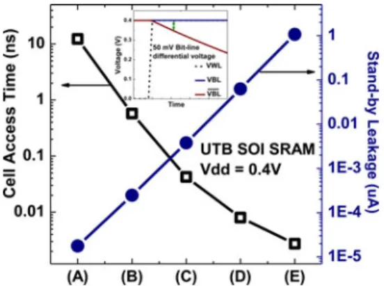
Fig. 6. “Cell” Read access time and stand-by leakage comparisons at Vdd = 0.4 V. Inset shows the definition of “cell” access time.
Fig. 7. Time-to-Write comparison at Vdd = 0.2, 0.3, 0.4 V. Inset shows the definition of time-to-write.
As V
dddecreases, the difference in WSNM from case (A) to case
(E) becomes smaller because transistors operate mostly in the
subthreshold region.
C. “Cell” Read Access Time
“Cell” read access time and time-to-write are analyzed by
connecting a column of 64 UTB SOI 6T SRAM cells (64 cells
age, thus trading off standby leakage with performance. Case
(D) with quarter band gap work function and lower (yet
ad-equate) threshold voltage has higher drain current and shows
around three orders of magnitude lower “cell” read access time
and higher standby leakage than case (A). Case (E), with
|V
th|
= 0.09 V (near bandedge work function), has lowest “cell” read
access time. However, it suffers severe RSNM degradation as
shown in Fig. 4.
D. Time-to-Write
For write operation, the “cell” write time is defined as the
time from the 50% activation of the word-line to the time when
the voltages of two cell storage nodes cross each other (see the
inset in Fig. 7). Fig. 7 shows the time-to-write comparison for
UTB SOI SRAM cells near the subthreshold region. UTB SOI
SRAM with lower V
thdevices (case D, |Vth| = 0.19 V) shows
much lower time-to-write than case (A).
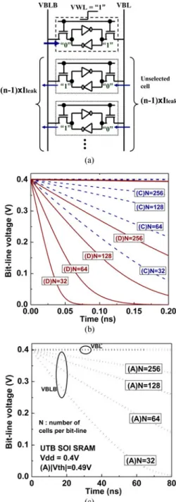
E. Cell Leakage
UTB SOI MOSFET, due to its better short-channel effects,
lower subthreshold swing, and reduced RDF, significantly
re-duces the leakage compared with Bulk CMOS devices. Fig. 8(a)
shows the worst case bit-line cell data pattern for read
opera-tion. All unselected cells (enclosed by dotted lines) have stored
logic value opposite to that of the selected cell (enclosed by
dashed line). The leakage through pass-gate transistors of the
unselected cells rivals the read current of the selected cell to
charge up the low-going bit line, while discharge the bit line
which is supposed to be held at “high.” Thus, the bit-line
differ-ential voltage is reduced, resulting in the degradation of sensing
margin and speed. Fig. 8(b) and (c) shows the bit-line voltage
versus sensing time with various number of cells per bit-line for
case (D) (solid line), (C) (dash line), and (A) (dot line) at V
dd= 0.4 V. For case (D) with
|V
th| = 0.19 V, the bit-line voltage
difference can be seen to develop significantly faster than case
(C) and case (A). Although case (D) has larger bit-line leakage
than case (A), case (D) can still support adequately large
num-ber of cells per bit-line (e.g., 256 cells per bit-line) due to its
larger read current and the well controlled short-channel effects
and superior leakage of UTB SOI MOSFETs. The real density
constraint comes from the overall leakage and power for the
intended subthreshold applications.
Fig. 8. (a) Worst case bit-line cell data pattern for Read operation. (b) Bit-line voltage versus sensing time with various number of cells per bit-line for case (D) (solid line), case (C) (dash line), and case (A) (dot line) at Vdd = 0.4 V. N is the number of cells per bit-line. (c) Bit-line voltage versus sensing time for case (A) (dot line) in expanded time scale at Vdd = 0.4 V.
IV. C
IRCUITT
ECHNIQUES FORS
TABILITY ANDL
EAKAGEI
MPROVEMENTSection III demonstrates that using the lower V
thdevices
(case D,
|V
th| = 0.19 V) significantly improves the WSNM
and offer higher performance while trading off leakage for the
subthreshold SRAM applications. This section evaluates the
ef-fectiveness of commonly used circuit techniques, such as
word-line voltage lowering [22], bit-word-line precharge voltage
lower-ing [17], and negative bit-line voltage [18]–[20], [23], [24], for
improving the stability, standby leakage, and write ability of
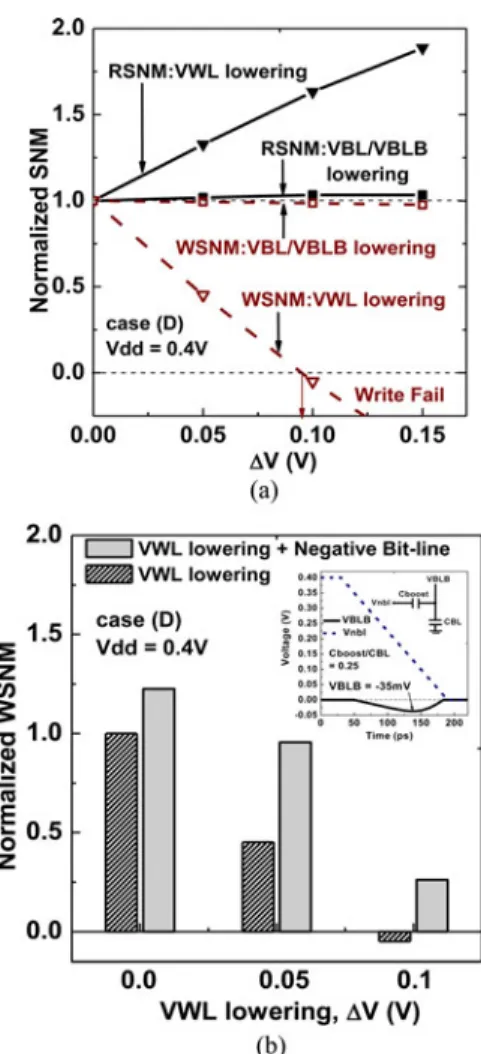
Fig. 9. (a) Impact of word-line voltage lowering (VWL = Vdd – ΔV) and bit-line precharge voltage lowering (VBL/VBLB = Vdd–ΔV) on the RSNM/WSNM, respectively. (b) Impact of the word-line voltage lowering on the normalized WSNM with and without using negative bit-line voltage tech-nique, respectively. Inset shows the negative bit-line voltage is−35mV.
the UTB SOI ultralow voltage SRAM cell with lower V
thde-vices (case D). Fig. 9(a) shows the impact of word-line voltage
lowering and bit-line precharge voltage lowering on the
nor-malized RSNM/WSNM, respectively. Lowering the word-line
voltage reduces the strength of pass-gate transistors, thus
improving RSNM and degrading WSNM. Lowering bit-line
precharge voltage reduces the read-disturb voltage (V
read, 0),
hence improving RSNM. On the other hand, during write
op-eration, the bit-line that is supposed to stay at “high” is held
at lower voltage level, thus degrading the push–pull write
ef-fect and WSNM. For the subthreshold SRAM operation,
low-ering word-line voltage shows larger improvement in RSNM
than lowering bit-line precharge voltage. RSNM improves by
33% as VWL is lowered by 50 mV (ΔV = 0.05 V).
How-ever, the word-line voltage lowering also significantly degrades
WSNM. The degraded WSNM can be mitigated using negative
bit-line (NBL) technique [18]–[20] where a capacitively
cou-pled transient negative pulse is introduced into the low-going
bit line to facilitate write operation. Fig. 9(b) illustrates that
using word-line voltage lowering (ΔV = 0.05 V) and negative
bit-line voltage (VBLB = –35 mV) show comparable WSNM
Fig. 10. Impact of bit-line precharge voltage lowering on the normalized standby leakage. Inset shows the impact of bit-line precharge voltage lowering on the normalized RSNM/WSNM.
as compared with the case without word-line voltage lowering
(ΔV = 0 V). In other words, using negative bit-line voltage in the
write operation can compensate for the WSNM degradation due
to word-line voltage lowering. Fig. 10 shows the impact of
bit-line precharge voltage lowering on the standby leakage. As the
bit-line precharge voltage is lowered by 50 mV (ΔV = 0.05 V),
the standby leakage is reduced by 20%. Therefore, using lower
V
thdevices (case D) with word-line voltage lowering, bit-line
precharge voltage lowering, and negative bit-line voltage can
enhance RSNM, reduce standby leakage, and improve WSNM
and write ability of UTB SOI SRAMs for ultralow voltage near
subthreshold opeartion.
V. V
ARIABILITY OFRSNM/WSNM C
OMPARISONFig. 11 shows the RSNM/WSNM characteristics for case (A)
and case (D) 6T UTB SOI SRAM cells considering
line-edge-roughness (LER) at V
dd= 0.4 V. For the lightly doped UTB
SOI MOSFETs we used in this study (gate length = 40 nm,
channel thickness = 10 nm), gate LER is the dominate
varia-tion source [25]. To assess the LER in UTB SOI MOSFETs,
the line edge patterns were derived using the Fourier
synthe-sis approach [21] with correlation length = 20 nm and rms
amplitude = 1.5 nm. Monte Carlo simulations with 150
sam-ples were performed for each case. The insets in Fig. 11(a)
and (b) are the log(Id)–Vg characteristics considering LER for
case (A) and case (D), respectively. As can be seen, case (D)
shows smaller drain current variation as its operation region
moves slightly into the super-threshold region. Thus, case (D)
shows smaller variation in RSNM and WSNM. Fig. 12 shows
the RSNM and WSNM variability comparison between case
(A) and case (D). For read operation, case (D) with smaller V
thshows 41% improvement in σRSNM and comparable mean of
RSNM as compared with case (A) [see Fig. 12(a)]. For Write
operation, case (D) shows 67% improvement in σWSNM and
84% improvement in the mean of WSNM as compared with
case (A) [seeFig. 12(b)].
Fig. 11. RSNM/WSNM characteristics consider line-edge-roughness for (a) case A (|Vth| = 0.49 V) and (b) case D (|Vth| = 0.19 V). Inset shows the log(Id)–Vg characteristics for case A and D considering LER. (Correlation length = 20 nm, Rms amplitude = 1.5 nm).
VI. C
ONCLUSIONWe have investigated the impact of threshold voltage design
on the stability, margin, performance, and variability of UTB
SOI 6T SRAM cells operating near the subthreshold region.
Our results indicated that UTB SOI 6T SRAM cell using lower
V
thdevices (
|V
th| = 0.19 V, V
dd= 0.4 V) showed comparable
RSNM, 84% improvement in WSNM, and significant
improve-ment in variability (σRSNM, σWSNM) as compared with that
using the higher V
thdevices (
|V
th| = 0.49 V, V
dd= 0.4 V).
For the UTB SOI 6T SRAM cells using lower V
thdevices,
the “cell” access time improved significantly with
correspond-ingly higher standby leakage. Lowering word-line voltage by
50 mV resulted in 33% improvement in RSNM while
degrad-ing WSNM simultaneously. Usdegrad-ing NBL voltage in the write
operation could compensate for the WSNM degradation due to
word-line voltage lowering. Lowering bit-line precharge
volt-age by 50 mV reduced the standby leakvolt-age by 20%. Our study
suggest that the lower V
thUTB SOI devices not only support
the high performance applications but also offer higher
perfor-mance and improve the stability/variability for ultralow voltage
near subthreshold SRAM applications.
Fig. 12. (a)RSNM variability (σRSNM considering LER) comparison be-tween case (A) and (D). (b) WSNM variability (σWSNM considering LER) comparison between case (A) and (D). Case (D) shows smaller variation due to its operation region slightly getting into the super-threshold region.
R
EFERENCES[1] J. Kim and K. Roy, “Double Gate-MOSFET subthreshold circuit for ul-tralow power applications,” IEEE Trans. Electron Devices, vol. 51, no. 9, pp. 1468–1474, Sep. 2004.
[2] B. H. Calhoun and A. P. Chandrakasan, “Static noise margin variation for sub-threshold SRAM in 65-nm CMOS,” IEEE J. Solid-State Circuits, vol. 41, no. 7, pp. 1673–1679, Jul. 2006.
[3] S. Monfray, M. P. Samson, D. Dutartre, T. Ernst, E. Rouchouze, D. Renaud, B. Guillaumot, D. Chanemougame, G. Rabille, S. Borel, J. P. Colonna, C. Arvet, N. Loubet, Y. Campidelli, J. M. Hartmann, L. Vandroux, D. Bensahel, A. Toffoli, F. Allain, A. Margin, L. Clement, A. Quiroga, S. Deleonibus, and T. Skotnicki, “Localized SOI technology: An innovative low cost self aligned process for ultrathin Si-film on thin BOX integration for low power applications,” in Proc. IEEE. Int. Electron
Devices Meet. Tech. Dig., 2007, pp. 693–696.
[4] T. Ohtou, N. Sugii, and T. Hiramoto, “Impact of parameter variations and random dopant fluctuations on short channel fully depleted SOI MOSFETs with extremely thin BOX,” IEEE Electron Device Lett., vol. 28, no. 8, pp. 740–742, Aug. 2007.
[5] Y. Morita, R. Tsuchiya, T. Ishigaki, N. Sugii, T. Iwamatsu, T. Ipposhi, H. Oda, Y. Inoue, K. Torii, and S. Kimura, “Smallest Vth variability achieved by intrinsic silicon on thin BOX (SOTB) CMOS with single metal gate,” in Proc. Symp. VLSI Tech. Dig., 2008, pp. 166–167. [6] X. P. Wang, C. Shen, M.-F. Li, H. Y. Yu, Y. Sun, Y. P. Feng, A. Lim,
H. W. Sik, A. Chin, Y. C. Yeo, P. Lo, and D. L. Kwong, “Dual metal gates with band-edge work functions on novel HfLaO high-k gate dielectric,” in Proc. Symp. VLSI Tech. Dig., 2006, pp. 9–10.
[7] V. Narayanan, V. K. Paruchuri, N. A. Bojarczuk, B. P. Linder, B. Doris, Y. H. Kim, S. Zafar, J. Stathis, S. Brown, J. Arnold, M. Copel, M. Steen,
gate n-MOSFETs using cap layers containing Group II A and III B ele-ments with gate-first processing for 45 nm and beyond,” in Proc. Symp.
VLSI Tech. Dig., 2006, pp. 178–179.
[8] H. N. Alshareef, H. R. Harris, H. C. Wen, C. S. Park, C. Huffman, K. Choi, H. F. Luan, P. Majhi, B. H. Lee, R. Jammy, D. J. Ichtenwalner, J. S. Jur, and A. I. Kingon, “Thermally stable N-metal gate MOSFETs using la-incorporated HfSiO dielectric,” in Proc. Symp. VLSI Tech. Dig., 2006, pp. 7–8.
[9] C. Fenouillet-Beranger, S. Denorme, B. Icard, F. Boeuf, J. Coignus, O. Faynot, L. Brevard, C. Buj, C. Soonekindt, J. Todeschini, J. C. Le-Denmat, N. Loubet, C. Gallon, P. Perreau, S. Manakli, B. Minghetti, L. Pain, V. Arnal, A. Vandooren, D. Aime, L. Tosti, C. Savardi, M. Broekaart, P. Gouraud, F. Leverd, V. Dejonghe, P. Brun, M. Guillermet, M. Aminpur, S. Barnola, F. Rouppert, F. Martin, T. Salvetat, S. Lhostis, C. Laviron, N. Auriac, T. Kormann, G. Chabanne, S. Gaillard, O. Belmont, E. Laffosse, D. Barge, A. Zauner, A. Tarnowka, K. Romanjec, H. Brut, A. Lagha, S. Bonnetier, F. Joly, N. Mayet, A. Cathignol, D. Galpin, D. Pop, R. Delsol, R. Pantel, F. Pionnier, G. Thomas, D. Bensahel, S. Deleonibus, T. Skotnicki, and H. Mingam, “Fully-depleted SOI technology using high-k and single-metal gate for 32 nm node LSTP applications featuring 0.179um2 6T-SRAM bitcell,” in Proc. IEEE. Int. Electron Devices Meet.
Tech. Dig., 2007, pp. 267–270.
[10] S. Kubicek, T. Schram, V. Paraschiv, R. Vos, M. Demand, C. Adelmann, T. Witters, L. Nyns, L.-A. Ragnarsson, H. Yu, A. Veloso, R. Singanamalla, T. Kauerauf, E. Rohr, S. Brus, C. Vrancken, V. S. Chang, R. Mitsuhashi, A. Akheyar, H.-J. Cho, J. C. Hooker, B. J. O’Sullivan, T. Chiarella, C. Kerner, A. Delabie, S. Van Elshocht, K. De Meyer, S. De Gendt, P. Absil, T. Hoffmann, and S. Biesemans, “Low VT CMOS using doped
Hf-based oxide, TaC-based metals and laser-only anneal,” in Proc. IEEE.
Int. Electron Devices Meet. Tech. Dig., 2007, pp. 49–52.
[11] M. Kadoshima, T. Matsuki, N. Mise, M. Sato, M. Hayashi, T. Aminaka, E. Kurosawa, M. Kitajima, S. Miyazaki, K. Shiraishi, T. Chikyo, K. Yamada, T. Aoyama, Y. Nara, and Y. Ohji, “Improved FET charac-teristics by laminate design optimization of metal gates —Guidelines for optimizing metal gate stack structure,” in Proc. Symp. VLSI Tech. Dig., 2008, pp. 48–49.
[12] J. Petry, G. Boccardi, R. Singanamalla, C. S. Liu, K. Xiong, P. Escanes, J.-L. Huguenin, J. Tseng, L. Van Nimwegen, F. Voogt, C. W. T. Bulle-Lieuwma, and M. Muller, “A VF B tunable single metal single dielectric
approach using As I/I into TiN/HfO2 for 32 nm node and beyond,” in
Proc. Int. Symp. VLSI-TSA, Apr. 2009, pp. 57–58.
[13] V. P.-H. Hu, Y.-S. Wu, M.-L. Fan, P. Su, and C.-T. Chuang, “Design and analysis of ultrathin body SOI based subthreshold SRAM,” in Proc. Int.
Symp. Low Power Electron. Design, 2009, pp. 9–14.
[14] V. P.-H. Hu, Y.-S. Wu, M.-L. Fan, P. Su, and C.-T. Chuang, “Static noise margin of ultrathin-body SOI subthreshold SRAM cells—An assessment based on analytical solutions of Poisson’s equation,” IEEE Trans. Electron
Devices, vol. 56, no. 9, pp. 2120–2127, Sep. 2009.
[15] V. P.-H. Hu, M.-L. Fan, P. Su, and C.-T. Chuang, “Impact of work function design on the stability and performance of ultrathin-body SOI subthreshold SRAM,” in Proc. Eur. Solid-State Device Res. Conf., 2009, pp. 145–148. [16] “ISE TCAD Rel. 10.0 Manual,” DESSIS, 2004.
[17] A. Bhavnagarwala, S. Kosonocky, C. Radens, K. Stawiasz, R. Mann, Q. Ye, and K. Chin, “Fluctuation limits and scaling opportunities for CMOS SRAM cells,” in Proc. Int. Electron Devices Meet. Tech. Dig., 2005, pp. 659–662.
[18] D. P. Wang, H. J. Liao, H. Yamauchi, Y. H. Chen, Y. L. Lin, S. H. Lin, D. C. Liu, H. C. Chang, and W. Hwang, “A 45 nm dual-port SRAM with write and read capability enhancement at low voltage,” in Proc. IEEE Int.
SOC Conf., 2007, pp. 211–214.
[19] S. Mukhopadhyay, R. Rao, J. J. Kim, and C. T. Chuang, “Capacitive cou-pling based transient negative bit-line voltage (Tran-NBL) scheme for improving write-ability of SRAM design in nanometer technologies,” in
Proc. IEEE Int. Symp. Circuits Syst., 2008, pp. 384–387.
[20] M. Yabuuchi, K. Nii, Y. Tsukamoto, S. Ohbayashi, Y. Nakase, and H. Shinohara, “A 45 nm 0.6 V cross-point 8 T SRAM with negative biased read/write assist,” in Proc. Symp. VLSI Circuit Dig., 2009, pp. 158–159. [21] A. Asenov, S. Kaya, and A. R. Brown, “Intrinsic parameter fluctuations in
decananometer MOSFETs introduced by gate line edge roughness,” IEEE
Trans. Electron Devices, vol. 50, no. 5, pp. 1254–1260, 2003.
[22] K. Nii, M. Yabuuchi, Y. Tsukamoto, S. Ohbayashi, S. Imaoka, H. Makino, Y. Yamagami, S. Ishikura, T. Terano, T. Oashi, K. Hashimoto, A. Sebe,
pp. 180–191, Jan. 2008.
[23] K. Nii, M. Yabuuchi, Y. Tsukamoto, S. Ohbayashi, Y. Oda, K. Usui, T. Kawamura, N. Tsuboi, T. Iwasaki, K. Hashimoto, H. Makino, and H. Shinohara, “A 45-nm single-port and dual-port SRAM family with robust read/write satbilizing circuitry under DVFS environment,” in Proc.
Symp. VLSI Circuit Dig., 2008, pp. 212–213.
[24] Y. Fujimura, O. Hirabayashi, T. Sasaki, A. Suzuki, A. Kawasumi, Y. Takeyama, K. Kushida, G. Fukano, A. Katayama, Y. Niki, and T. Yabe, “A configurable SRAM with constant-negative-level write buffer for low-voltage operation with 0.149um2Cell in 32 nm high-k metal gate CMOS,”
in Proc. IEEE Int. Solid-State Circuits Conf., 2010, pp. 348–350. [25] T. Ohtou, N. Sugii, and T. Hiramoto, “Impact of parameter variations and
random dopant fluctuations on short-channel fully depleted SOI MOS-FETs with extremely thin BOX,” IEEE Electron Device Lett., vol. 28, no. 8, pp. 740–742, Aug. 2007.
Vita Pi-Ho Hu (S’09–M’13) received the Ph.D. de-gree from the Department of Electronics Engineer-ing and Institute of Electronics, National Chiao Tung University, Hsinchu, Taiwan, in 2011.
She is currently an Assistant Researcher with Na-tional Chiao Tung University.
Ming-Long Fan (S’09) was born in Taichung, Tai-wan, in 1983. He received the B.S. degree from the Department of Electrical and Control Engineering, the M.S. degree from the Department of Electron-ics Engineering, National Chiao Tung University, Hsinchu, Taiwan, in 2006 and 2008, respectively, where he is currently working toward the Ph.D. de-gree in the Institute of Electronics.
His current research interests include de-sign and modeling of subthreshold SRAM in scaled/exploratory technologies.
Pin Su (S’98–M’02) received the B.S. and M.S. de-grees in electronics engineering from National Chiao Tung University, Hsinchu, Taiwan, and the Ph.D. de-gree from the Department of Electrical Engineering and Computer Sciences, University of California at Berkeley, Berkeley, USA.
From 1997 to 2003, he conducted his doctoral and postdoctoral research in Silicon-On-Insulator (SOI) devices at Berkeley. He was also one of the major contributors to the unified BSIMSOI model, the first industrial standard SOI MOSFET model for circuit design. Since August 2003, he has been with the Department of Electronics Engineering, National Chiao Tung University, where he is currently a Pro-fessor. His research interests include silicon-based nanoelectronics, modeling, and design for exploratory CMOS devices for ultra-low-power applications, and circuit-device interaction and cooptimization in nanoscale CMOS. He has authored or coauthored more than 160 research papers regarding his research interests in refereed journals and international conference proceedings.
Prof. Su serves in the technical committee of the IEEE International Electron Devices Meeting (IEDM).
a Manager of the Bipolar VLSI Design Group, working on low-power bipolar circuits, high-speed high-density bipolar SRAMs, multi-Gb/s fiber-optic data-link circuits, and scaling issues for bipolar/BiCMOS devices, and circuits. Since 1988, he has been managing the High Performance Circuit Group, investigating high-performance logic and memory circuits. Since 1993, his group has been primarily responsible for the circuit design of IBM’s high-performance CMOS microprocessors for enterprise servers, PowerPC workstations, and game/media processors. Since 1996, he has been leading the efforts in evaluating and ex-ploring scaled/emerging technologies, such as PD/SOI, UTB/SOI, strained-Si devices, hybrid orientation technology, and multigate/FinFET devices, for high-performance logic, and SRAM applications. Since 1998, he has been responsible for the research VLSI Technology circuit codesign strategy, and execution. His group has also been very active and visible in leakage/variation/degradation tol-erant circuit and SRAM design techniques. He has authored many invited papers in international journals such as International J. of High Speed Electronics, Pro-ceedings of IEEE, IEEE Circuits and Devices Magazine, and Microelectronics Journal. He holds 50 U.S. patents with another 20 pending. He has authored or coauthored more than 350 papers.
Short Course, ISQED, ICCAD, APMC, VLSI-DAT, ISCAS, MTDT, WSEAS, VLSI Design/CAD Symposium, and International Variability Characterization Workshop. He was the corecipient of the Best Paper Award at the 2000 IEEE International SOI Conference.