Ching-Fa Yeh,c Shyue-Shyh Linf and Water Lurb
aDepartmefltof Electronic Engineering, National Chiao Tung University, Hsinchu, Taiwan 'United Microelectronics Corporation, Hsinchu, Taiwan
ABSTRACT
To develop a low-stress dielectric thin film, a novel liquid-phase deposition (LPD) technique utilizing silica-saturat-ed hydrofluosilicic (H2SiF6) solution with only H20 addsilica-saturat-ed is propossilica-saturat-ed. Due to fluorine incorporation, the stress in as-deposited LPD oxide can he as low as 83.3 MPa (tensile). Addition of 1120 greatly affects the stresses in as-as-deposited LPD oxide: the less 1120 added, the lower the stress will be. The stress variations accompanying thermal cycling have also been clarified. Films deposited with a larger quantity of H20 added exhibited larger stress variations (hysteresis). After ex situ annealing at around 600°C, the total stress decreased to near 0 MPa.
To meet future high-density and high-performance
requirements for ultralarge scale integration (ULSI)
de-vices, multilevel interconnection has become more im-portant than ever. For multilevel interconnection,
low-temperature formation of fully planarized interlayer
dielectric film is a key technology. To realize this technol-ogy, a selective deposition method that is independent of the pattern aspect ratio is essential.1In addition to planarization, stress in interlayer dielec-tric films also has significant effects on the reliability of multilevel interconnections.2 Excessive stress in dielectrics makes films crack easily and/or delaminate,3 or induces voids in the interconnections.45 To develop a reliable inter-layer dielectric film for multilevel interconnection, inves-tigation into film stress is indispensable.
Recently, a newly developed liquid-phase deposition
(LPD) technique has been shown to be capable of selectiv-ity depositing silicon oxide films at room temperature.1'6
Excellent physicochemical and electrical properties of
LPD oxide have also been reported.7'8 In particular, it has been found that fluorine atoms can be incorporated natu-rally, into the LPD oxide during deposition.9 Therefore, the LPD method is potentially applicable to the formation
of interlayer dielectric films for multilevel
interconnec-tion. In a previous study,9 we reported that the quantity of 1130 added can greately affect the physicochemical prop-erties of LPD oxide. However to date, stress in LPD oxide
has not been investigated. In this paper, the effects of
added 1130 on stresses in LPD oxide are investigated in detail. Variations in stresses in LPD oxide during in situ and ex situ thermal cycling are also clarified.
Oxide
StressOxidestress (CT) has two components, intrinsic stress (o,,) and thermal stress (oth), i.e.
= gin + 0, [1]
The intrinsic stress component results mainly from
bonding between Si, 0, and OH, and can be either tensile
or compressive. The thermal stress component, on the other hand, is attributable to a difference in thermal
ex-pansion coefficients between films and substrates that can cause differential contraction during cooling from deposi-tion temperature to ambient temperature, and is given byu
= E1/U —v1)
5 d( —
ajdT
[2]where E1 is the Young modulus for the film, v1 is the
Poission ratio of the film, a1 and a, are the thermal
expan-sion coefficients of, respectively, the substrates and the
films, and 74 and Ta are, respectively, the deposition and stress-meausrement temperatures. In the case of Si03 film on Si substrates, E1/(1—v6) is equal to 8.5 >< 1011 dyn/cm2, and if a1 and a, do not change with temperature, then the
above equation can be simplified to
= [_..u_J
(crca,) (T Ta)
1—v1
Since a, (3.0 >< 10-6 °C1) is usually larger than af (0.55 X l0 ac_i) is for SiO2 films on Si substrates, and Td is usu-ally larger than Ta, the resulting stress become compres-sive at room temperature.
Experimental
Samplepreparation—Four inch p-type (100) 15 -_25
CI-cm silicon wafers were used as substrates in all
experi-ments. The wafers were cleaned using standard processes and the native oxide that formed during cleaning (HO + 11202 + 1120) was not removed. The initial radius of curva-ture of each wafer was measured by means of a
single-laser reflection technique employing a Tencor FLX-2320 thin-film stress-measurement instrument.
An aqueous solution consisitng of 75 g of 99.99% pure silica powder added to 1750 ml of 4 mol/liter hydrosilico-fluoric acid (H2SiF6) was prepared and saturated with sili-cic acid [Si(OH)4].9 To supersaturate the solution,
deion-ized water (1130) was later added as described below. The prepared wafers were immersed in solutions con-taining 250 —750ml of added 1120 per 1000 ml of saturat-ed solution to deposit 1700 A thick LPD oxide films. The deposition temperature of 25°C was carefully controlled by means of water bath and immersion times (shown in the table inset in Fig. 1) were varied according to the amount of 1130 added to control oxide thickness.
In preparation for stress measurements, film deposited
on the back sides of wafers was stripped away using a
buffered HF solution.
Stress measurements —Stresses in deposited oxides were calculated by determining changes in wafer radii of curva-ture after deposition according to the following equation11'12
where E, and v, are, respectively, the Young modulus and Poisson ratio of Si, t6 and t, are the thickness of the LPD oxide and Si substrate, respectively, and R1 and R2 are, respectively, the wafer radii of curvature before and after LPD oxide deposition.
To clarify the LPD oxide stress variations during in situ thermal cycling, periodic stress measurements were made as wafers with LPD oxide films were heated from 25 to 450°C in an N2 atmosphere at a ramped rate of 8.5°C/mm,
then cooled back down to 25°C at 1.6°C/mm. Separate
stress measurements were made after reheating the ther-mally cycled wafers to 450°C in N2 ambient for 30 mm to
check the final equilibrated stresses. And since during
actual processing the stresses built up by annealing may exert a significant impact on interconnections,13 2200 A thick LPD oxide films made with 375 and 750 ml of added 1120 per 1000 ml of saturated solution were heat-treated
ex situ at 400 1000°C in N2 ambient for 30 mm, with stress measurements being made immediately after each treatment.
[3] Finally, to determine fluorine concentrations in the top
layers of LPD oxides after all annealings, x-ray
photo-E,
(t
6(1-v,)
(1
1 1i?2 R3
[4]
electron spectroscopy (XPS) was performed at a single take-off angle using a Perkin-Elmer Model 1600 spec-trometer.
Resultsand Discussion
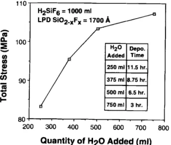
LPD oxide stress.—Figure 1 shows the dependence of stress on the quantity of added H,0 for 1700 A thick LPD oxides. All the stresses were found to be tensile and to pos-sess magnitudes ranging from 80 to 110 MPa. These values are much lower than the 200 -500MPa of CVD oxides.'4-16 In this figure, we can also see that the stress shows a strong dependence of the quantity of added 1120.
Since the deposition and measurement temperatures are nearly the same (room temperature), the total stress in
as-deposited LPD oxide must result mainly from intrinsic
stress. The intrinsic stress in LPD oxide may be caused by
bond strains originating from the dehydration reaction during deposition. When Si-0-Si bonding takes place
after dehydration, there must be a large puckering strain.'2
If sufficient energy is not applied to the oxide, bond
strains will remain and result in intrinsic stress. Since the
dehydration reaction causes shrinkage of the film, the
intrinsic stress must be tensile."
LPD oxide deposited with 250 ml of 1120 added shows a stress of 83.3 MPa, while films deposited with 375 and 500 ml of H20 added show stresses near 103.3 MPa.
However, the film deposited with 750 ml of 1120 added
only shows a slight increase in comparison with that
deposited with 500 ml of H20 added, leading to the con-clusion that the less 1120 added, the lower the stress was in the LPD oxide. The lower stress may be due to the effect of fluorine atoms incorporated in the film. We reported in our previous study that the less 1120 added to the solution, the more fluorine atoms were likely to be incoporated into the LPD oxide.'9 The stress could be reduced by increased fluorine incorporation in the oxide."'2 A possible
mecha-nism leading to the stress reduction is the interaction of fluorine atoms with strained Si-0 bonds, forming Si-F
and nonbridging bonds, which result in local strain relax-ations.23 Thus, the lower stresses in LPD oxides deposited
with less H20 added can be attributed to an increase in
fluorine atoms incorporated in the films.
The discussion above suggests that the stress in LPD
oxide should increase linearly with increasing quantities of added 1120 because fluorine atoms incorporated in the LPD oxide are decreasing linearly with increased quanti-ties of added 11,0." However, in Fig. 1, we see that there is only a slight increase in stress in samples deposited with 750 ml of 1120 added. The relatively minor difference in
(U
0.
U, U, (U1
a'
U) (Ua'
0
I-.Quantity of H20 Added (ml)
Fig. 1. Dependence of stress on the quantity of H20 added for
1700 A thick LPD oxides. The inset shows the deposition time used
to yield the oxide thickness for different quantitites of added H20.
stress may be due to many more OH-related bonds
con-tained in films prepared with 750 ml of H,0 added,
because tensile stress is reduced when OH-related bonds are present.24" Why more OH-related bonds are containedin films with larger quantities of added 1120 can be
ex-plained as follows: when H,0 is added to a saturated
H,SiF, solution, the silicic monomer Si(OH)4 is formed and then absorbed by the substrate surface. Acid-catalyticdehydration occurs between these silicic monomers, fol-lowed by Si-O-Si bond formation. The more 1120 added, the less likely the dehydration reaction is to be complete-ly finished in time, and the larger the number of residual OH bonds remaining in the film. However, since it is
diffi-cult to quantify OH-related bonds contained in LPD
oxides, we cannot directly prove these inferences at pre-sent; work on quantifying OH-related bonds in LPD oxide is still in progress.Stress variation during in situ thermal
cycling—Varia-tions in total stress during in situ thermal cycling for
1700 A thick LPD oxides prepared with 75, 500, 375, and 250 ml of H20 added are shown in Fig. 2a-d, respectively.
It should be noted that the p-axis scales in these figures
are not the same for all four samples. The samples all show
that total stress tends to become more tensile when the
annealing temperature is increased to 450°C. During the subsequent cooling cycling, the total stress become less tensile with decreasing temperature, but the final value of total stress in thermal annealing is larger than the initial value. That is, the total stress variation shows hysteresis over the course of thermal cycling. As mentioned above, total stress in thin film includes two components: thermal
stress and intrinsic stress. During thermal cycling, both
thermal stress and intrinsic stress may change with
tem-perature. According to Eq. 3, thermal stress has a linear
relationship with temperature, and becomes more tensile
as temperature increases, less tensile as temperature
decreases. If no intrinsic stress developed in the filmdur-ing thermal cycldur-ing, the variation in total stress should
follow the linear variation in thermal stress only, and show no hysteresis. However, the hysteresis shown in Fig. 2 sug-gests that some intrinsic stress developed in the LPD oxide during thermal cycling.
The development of intrinsic stress in LPD oxide during thermal cycling is due to changes in the oxide structure, especially the escape of OH-related bonds, and formation of additional Si-O-Si bonds. Si-O-Si bond formation can
give rise to a large number of bond strains. If the bond
strains are not relieved, they will result in intrinsic tensile stress in the film. With increasing temperature, an increase
in intrinsic tensile stress can develop in the oxide, and
consequently make the total stress more tensile. If a large intrinsic tensile stress is left in the film at the beginning of the subsequent cooling cycle, it will remain constant with decreasing cooling temperature. Thus, the combination of
thermal stress and intrinsic stress will make total stress during cooling larger than that during heating, allowing hysteresis to occur.
The hysteresis scale can be calculated from the differ-ence between the initially measured stress and the finally equilibrated stress. The dependence of hysteresis stress in 1700 A thick LPD oxides on the quantity of added 1120 was calculated, and is shown in Fig. 3. In this figure, we
can clearly see that the more H,0 added, the greater the hysteresis. That is, in LPD oxide deposited with more 1120, a larger intrinsic stress developed during thermal cycling. Since the hysteresis is attributable to residual OH-related bonds, the results shown in Fig. 3 are consistent with the observation that more OH-related bonds are contained in LPD oxides deposited with larger quantities of added H2O. Stress variation during ex situ thermal cycling—Total stress (UT) in LPD oxide annealed ex situ was also investi-gated. The dependence of T on annealing temperature is shown in Fig. 4. Samples deposited with 375 and 750 ml of H,O added were compared, and it was found that both exhibited similar characteristics. The maximum tensile
V 100 H2SiF6 = 1000 ml LPD SiO2..xF = 1700 A H20 Added 250ml 375 ml! 500 ml 750 ml Depo. Time 11.5 hr. 8.75 hr. 6.5 hr. 3hr. 200
300 400
500600 700
800stress was found in films annealed at 400°C, with aT begin-ning to decrease with increasing temperatures over 400°C. It then decreased to compressive stress after annealing at
600°C. When the film was annealed at 800°C, the T
increased again. However, after annealing at 1000°C, the a.. decreased toward more compressive stress. This clearly indicates that intrinsic stress developed in the LPD oxide
film during ex situ thermal cycling probably owing to
structural changes. To study these structural changes fur-ther during fur-thermal cycling, variations in intrinsic stress (at,,) with temperature were obtained by subtracting the calculated thermal stress (th) from o., as shown in Fig. 5. The characteristics of a1,, are similar to those of a. except for the difference in scale.
As mentioned above, the OH-related bonds contained in the film escape with annealing at 400°C. Annealing causes the LPD oxide to undergo densification via the formation of additional Si-O-Si bonds, which can give rise to bond strains: If the bond strains are not relieved, intrinsic stress in the film increases. Thus, intrinsic stress increased after annealing at 400°C. Further increasing annealing temper-ature to 600°C gave structural atoms in the film sufficient energy to move locally. This not only caused bond
restruc-turing, but also relieved the bond strains, and hence,
reduced intrinsic tensile stress.13 There seems to exist a threshold temperature beyond which the intrinsic tensile stress in LPD oxide decreases.
The fact that intrinsic stress becomes increasingly more tensile again at annealing temperatures over 600°C may be accounted for by the removal of fluorine atoms from the
film. Fluorine removal allows reconfiguration of bonds and diminishes the relaxation effect of strained bonds,
resulting in increased intrinsic stress. The fact that
fluo-€5 a.
S
0) U, 4) I-4) .7;; >1r
U, U) 4)Quantity of H20 Added (ml)
800Fig. 3. Dependenceof total stress hysteresis on the quantity of
added 1120 for 1700 A thick LPD oxides. The hysteresis was calcu-lated from the difference between initial stress measurements and final equilibrium stress measurements.
H20=750ml
t0=iiooA
..
.
.
a U0e•
a0t
a Heating • Cooling -Wv 300 200 100 H20=375ml = 1700 A.
a • .• •fl1Cn•. •.• a
a %P.'e UDo
dI °
Heating • Cooling €5a.
S
U) U,.
U) (5a-S
(0 U, Cl) 500 400 300 200 100 400 300 200 100 0 100 200 300 400Temperature (°C)
(a)
500 U '5a-S
U) f0 (5a.
S
(0 U, 4, 7-U) 0 100 200 300 400 500Temperature (°C)
(C)
1120 = 500 mltoxl700A
..
•
• .
S a• ••.••
.•I
•
•
Ca
C•
0 0 a 0ag
a Heating • Cooling 300 200 100 1120 = 250 ml = 1700 A•
t
•••. c;1e•• .•• •n'•• • a
•.
•
aoaa..
cixpqj
a Heating . Cooling 0 100 200 300 400 500Temperature (°C)
(b)
U 0 100 200 300 400 500Temperature (°C)
(d)
Fig. 2. Variations in total stress during in situ thermal cycling (25 — 450°C) for 1700 A thick LPD oxides deposited with (a) 750, (b) 500,
(c) 375, and (d) 250 ml of 1120 added to 1000 ml of saturated H2SiF6 solution.
Fig. 4.Effects of ex situ thermal annealingtemperatureontotal stressfor 2200 A thick LPDoxides.Two sampleswith different
quantities of H20 added are shownforcomparison.
tine disappears from LPD oxide after annealing at 800°C
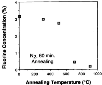
has been confirmed by XPS spectra investigation. As
shown in Fig. 6, fluorine concentrations in LPD oxides are greatly reduced after annealing over 700°C. As for anneal-ing at 1000°C, the effect of strained bond relief diminishes stress further, and results in decreased stress.
The variations in total stress during in situ thermal
cycling for LPD oxides with and without ex situ thermal annealing at 600°C were measured. As shown in Fig. 7, LPD oxide annealed at 600°C showed almost not
hystere-sis during in situ thermal cycling, but unannealed LPD
oxide showed slight hysteresis. This can also be attributed to the buildup and release of intrinsic stress in the films. In films annealed at 600°C, few OH-related bonds exist, and the intrinsic stress is relieved. In this case, even when the film was subjected to in situ thermal cycling, no fur-ther densification and increase in strained bond occurred, thus the intrinsic stress remained constant during thermal cycling. That is, only thermal stress variations occurred and very little stress hysteresis was observed. A few OH-related bonds were still contained in the as-deposited LPD oxide, and consequently, hysteresis occurred during in situ thermal cycling.
0
0 200 400 600 800 1000
Annealing Temperature (°C)
Fig. 6. Changes in fluorine concentration in[PD oxides annealed
at different temperatures.
Conclusions
Theeffects of quantities of added 1120 on stress in LPD oxides have been investigated. As-deposited LPD oxide film exhibited tensile stress as low as 83.3 MPa because of
low-temperature deposition and fluorine incorporation.
We also found that the less 1120 was added, the lower the stress was. This can be attributed to the greater number of fluorine atoms incorporated in the film.
A hysteresis stress phenomenon was observed when the LPD oxide film was subjected to in situ thermal cycling. Films deposited with larger quantity of H20 added exhib-ited greater hysteresis because they contained more OH-related bonds. Thus, LPD oxide deposited with less added 1120 will be more suitable for use as interlayer dielectrics in multilevel interconnections. In the case of ex situ ther-mal annealing, the intrinsic stress increased owing to the escape of OH (at 400°C) and the removal of F (at >600°C), while it decreased owing to bond strain relaxation (at
600°C and> 800°C). After annealing at around 600°C, the total stress is decreased to near 0 MPa.
Acknowledgment
This
study was supported by the National Science
Council, Republic of China, under Contract No. NSC85-Fig. 5. Effectsofex situ thermalannealingtemperatureon intrin-sic stress for 2200Athick LPDoxides.Two samples withdifferent quantities of added H20 areshownforcomparison.
0 100 200 300 400 500
Temperature (°C)
Fig. 7. Variations in total stressduring in situ thermal cycling (25 - 450°C) for [PD oxides with and without thermal annealing at 600°C in N2 for 30 mm.
0
a-0
0) 0)0
I-I.I
LPD S1O2..xFx = 2200 A - IOU 0 200 El 0 N2, 60 mm. Annealing0
400 600 800 1000Annealing Temperature (°C)
El 0) a-C') C') Cl) C,0
C L. C 400 300 200 100 0) a-C') U) 0) H2SIF6 = 1000 ml LPD SiO2.xF = 2200 A os 600°C, N2, 30 mm. Annealing a £ As-deposited a aa a
a Heating a a a a a Cooling a aA A a Aaaaa aa a
00 Maa aa aa
aAa 0aaaa'
•:"'
0 0 0 0 heating.
Cooling LPD Sb2 xF = 2200 A 0 200 400 600 800 1000Annealing Temperature (°C)
2215-E-009-057. A portion of the work was supported by the United Microelectronics Corporation (UMC).
Manuscript submitted Oct 27, 1995; revised manuscript received April 3, 1996.
National Chiao Tung University assisted in meeting the publication costs of this article.
REFERENCES
1. T. Homma, T. Katoh, Y. Yamada, and Y. Murao, This Journal, 140,2410(1993).
2. 5. Wolf, Silicon Processing for VLSI Era, Vol. 2, p. 195, Lattice Press, Sunset Beach, CA (1990).
3. ID. Temple, A. Reisman, G. G. Fountain, M. Walters, and S. V. Hattangady, This Journal, 140, 564 (1993). 4. T. D. Sullivan, Appl. Phys. Lett., 55, 2399 (1989). 5. K. Hinode, I. Asano, T. Ishiba, and Y. Homma, J. Vac.
Sci. Technol., B8, 495 (1990).
6. C. F Yeh and C. L. Chen, Semicond. Sci. Technol., 9, 1250 (1994).
7. C. F Yeh, '2. Z. Yang, and T. J. Chen, IEEE Trans. Electron Devices, ED-42, 307 (1995).
8. C. F Yeh, S. S. Lin, and T. Y. Hong, IEEE Electron Device Lett., EDL-16, 316 (1995).
9. C. F Yeh, C. L. Chen, and G. H. Lin, This Journal, 141, 3177 (1994).
10. K. Ramkumar and A. N. Saxena, ibid., 139, 1437 (1992). 11. B. Bhushan, S. P. Muratka, and J. Gerlach, J. Vac. Sci.
Technol., B8, 1068 (1990).
12. L. M. Mack, A. Reisman, and P. K. Bhattacharya, This Journal, 136, 3433 (1989).
13. K. Ramkumar, S. K. Ghosh, and A. N. Saxena, ibid., 140, 2669 (1993).
14. G. Smolinsky and T. P. H. F. Wendling, ibid., 132, 950 (1985).
15. M. Jarsoz, L. Kocsanyi, and J. Giber, Applications of Surface Science, 1982-1983, p. 122 North Holland, Amsterdam (1983).
16. C. Blaauw, J. Appl. Phys., 54, 5064 (1983).
17. W. A. Pliskin and R. A. Gdula, in Handbook on
Semiconductors, Vol. 3, T. S. Moss, Editor, p. 648, North-Holland Publishing Co., Amsterdam (1980).18. M. Nakamura, R. Kanazawa, and K. Sakal, This Journal, 133, 1167 (1986).
19. C. F. Yeh and C. L. Chen, ibid., 142, 3579 (1995). 20. D. Kouvatsos, J. G. Huang, and R. J. Jaccodine, ibid.,
138, 1752 (1991).
21. K. P Macwilliams, L. F Halle, and'2. C. Zietlow, IEEE Electron Device Lett., EDL-11, 3 (1990).
22. E. F Dasilva, Y. Nishioka, and'2. P Ma, IEEE Trans., Nucl. Sci., NS-34, 1190 (1987).
23. Y. Nishioka, K. Ohyu, Y. Ohji, N. Natuaki, K. Mukai, and T. P. Ma, IEEE Electron Device Lett., EDL-10,
141 (1989).
24. 5. Robles, E. Yieh, and B. C. Nguyen, This Journal, 142, 580 (1995).
25. H. Sunami, Y. Itoh, and K. Sato, J. Appl. Phys., 41,
5115 (1970).
Impurities in Chemical Bath Deposited CdS Films for
Cu(In,Ga)5e2 Solar Cells and Their Stability
A. Kylner,*0 J. Undgren,b and L StoltaaDepanment of Technology, Electronics, Solar Cells and bDepanment of Inorganic Chemistry, Uppsala University, S-751 21, Uppsala, Sweden
ABSTRACT
The highest efficiencies for Cu(In,Ga)Se2-based thin film solar cells have been achieved with CdS films prepared by a solution growth method known as the chemical bath deposition (CBD) technique. The impurity content in such cadmi-um sulfide films has been examined. By means of secondary ion mass spectroscopy, Fourier transform infrared spec-troscopy, Rutherford backscattering spectrometry, and x-ray photoelectron specspec-troscopy, we conclude that CBD grown CdS films contain —11 atom percent (a/o) 0, --.5 a/o N as well as C and H. Unlike previously published results, cadmium carbonate (CdCO3) and water (H20) are found to be the main oxygen-containing compounds. No clear evidence of cad-mium hydroxide [Cd(OH)2] and/or oxide (CdO) is found. Carbon-nitrogen bonds originating from any pseudohalogenic ions [e.g., cyanamide (NCN2), thiocyanate (SCN), cyanate (OCN), cyanide (CN)] are identified as the main nitrogen impurity. To investigate the stability of the impurities, the films were subjected to air annealing (200 to 350°C) as well as storage (1.5 month) in three different environments: desiccator, humidity of 79%, and at 100°C. Air annealing results in a decrease of the water content, which disappears at 350°C. On exposure to humidity, the water content increases some-what. The CN bonds are very sensitive to all treatments, but do not totally decompose, not even at 3 50°C. In contrast, CdCO3 is much more stable.
Introduction
CdSis a superior photosensitive semiconductor. It has found extensive applications in the field of optoelectronics (e.g., solar cells, semiconductor lasers, photocells, photo-conductive gas sensors, and infrared detectors). Thin films
of this semiconducting material can be deposited by a
variety of techniques, such as vacuum evaporation, sput-tering, spray pyrolysis, chemical vapor deposition (CVD), and electrodeposition. A relatively less common method is a chemical solution growth technique known as chemical bath deposition (CBD).
In the CBD technique, the film deposition is carried out
in an alkaline aqueous solution (pH >
10) containingthiourea [SC(NH2)2] and a cadmium complex [e.g., Cd(NH3)]. When ammonia is used as the complexing
agent, the overall reaction is assumed to bet
Cd(NH +
SC(NH2)2+2OW*Electrochemical Society Student Members.
-° CdS+H2NCN+4NE3+2H20 [1]
As an aqueous solution method, it presents many advan-tages: inexpensive, noncomplex equipment, low tempera-ture (<100°C) and large-area deposition. All these
proper-ties are well suited for the manufacture of photovoltaic devices.
For CdTe/CdS and Cu(In,,de2/CdS/ZnO thin film
solar cells, the chemical bath deposition shows anotherexcellent property. The highest efficiencies for both these cell structures57 have been achieved with CdS films pre-pared by this deposition technique.
The reason why CBD grown CdS gives a better photo-voltaic performance as compared to, e.g., evaporated CdS remains unclear. It has been suggested that a pinhole-free conformal coverage, low temperature deposition, or chem-ical treatment of the surface during the CBD process are of importance, but clear evidence has not been submitted.
There exists, however, another possibility: impurities