Electroluminescence at Si Bandgap Energy from
MetahOxide-Semiconductor Tunneling Diodes
Ching-Fuh Lin*, Miin-Jang Chen*, Ming-Hung Lee, and Cheewee Liu
Department ofElectrical Engineering, National Taiwan University, Taipei 106, Taiwan
Email: [email protected]
*
also
with Graduate Institute ofElectro-Optical Engineering
Abstract
We report room-temperature electroluninescence at Si bandgap energy from Metal-Oxide-Semiconductor (MOS) tunneling diodes. The Ultrathin gate oxide with thickness 1 3 urn was grown by rapid thennal oxidation (RTO) to allow significant current to tunnel through. The measured EL efficiency of the MOS tunneling diodes increases with the injection current and
could be in the order of iO, which exceeds the limitation imposed byindirect bandgap nature of Si. We also study the
temperature dependence ofthe electroluminescence and photoluminescence. The electroluminescence is much less dependent on temperature than photoluminescence from Si. The applied external field that results in the accumulation of majority carriers at Si/Si02 interface in the case of electroluminescence could be the reason for such difference. The involved physics such as optical phonon, interface roughness, localized carriers, and exciton radiative recombination are used to explain the electroluminescence from silicon MOS tunneling diodes.
Keywards —
Silicon,MOS, electroluminescence.1. Introduction
Silicon is the most important semiconductor material for electronics industry, but has limited applications in area ofoptics and optoelectromcs due to its indirect bandgap characteristics that make it hardly emit light. In order to convert silicon to a light-emitting materkil, many efforts had been tried before, including porous silicon, nanocrystalline Si, Si/Ge alloy, and
Erbium doping of Si, and so on '. However,this luminescence originates from the defect-related mechanisms and the fabrication processes are complicated. In this paper, we report efficient electroluninescence (EL) at Si bandgap from metal!
Si02!Si Metal-Oxide-Semiconductor tunneling diodes .Thecharacteristics of the light-emitting MOS tunneling diodes on silicon are
1 . Thestructure ofMOS tunneling diode is the same as that used in Ultra-Large-Scale-Integration (ULSI) circuits,
2. Using tunneling current through the ultrathin oxide (15 35A)to provide carriers for radiative recombination,
3 . Theemission wavelength is near silicon bandgap ,and
4. The fabrication processes are fully compatible with the present ULSI technology.
As a result, the light-emitting MOS tunneling diodes show promise to achieve the practical on-chip light source for optical interconnection and silicon-based optoelectromcs integrated circuits (OEIC).
The temperature dependence of electro- and photoluminescence (PL) was also investigated to study the luminescent properties of the silicon MOS tunneling diodes. The EL was found to be less dependent on temperature than PL from Si. The reason is attributed to the accumulation ofmajority carriers at Si! Si02 interface due to the applied external field in the EL case.
A physical process involving phonon assistance and exciton radiative recombination is used to fit the measured
electroluminescence spectra. The excellent match ofthe calculated spectrum to the measured data ofEL spectra shows that the exciton radiative recombination and the participation of optical phonon take place in the room-temperature EL from the silicon MOS tunneling diodes.
Silicon-basedand Hybrid Optoelectronics Ill, David J. Robbins, John A. Trezza, Ghassan E. Jabbour,
C G) C) G) 0)
2. Device Fabrication
When the devices are scaled down in the state-ofthe-art ULSI chips, ultra-thin gate oxides are needed to reduce short channel effects. However, current tunneling through the ultra-thin gate oxide inevitably increases when the thickness of the gate oxide shrinks with each generation ofIC fabrication technology. Therefore, the devices based on the tunneling current are fabricated and developed. In order to grow the high quality ultra-thin gate oxide, the rapid thermal oxidation (RTO) is commonly used to
meet this requirement .
In
this work, the MOS tunneling diode has the Ultrathin gate oxide to make significant current tunnel through. The ultrathin gate oxide was grown by rapid thermal oxidation (RTO) on n-type (100) Si wafer at 900 -1000°C .Theresistivity ofSi substrate are 11O U -cm. The gas flows are 500 sccm nitrogen and 500 sccm oxygen at a reduced pressure. The thickness
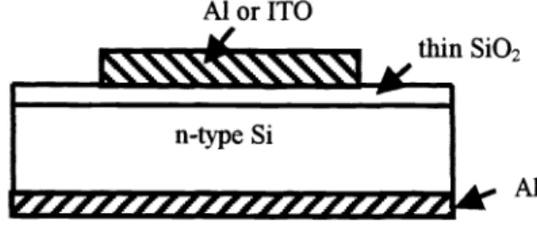
of oxide is measured by ellipsometry and confirmed by high-frequency capacitance-voltage measurements. The oxide thickness is in the range of 15 35A.Aluminum or transparent indium tin oxide (ITO) was deposited as the gate electrode using the usual evaporator. The gate electrodes with various circular areas are defined by photolithography. The thickness of Si substrate is about 500 tm and aluminum was deposited on the backside as another electrode of the MOS diode. The device structures are schematically shown in Fig. 1.
Al or ITO
thin Si02
Fig.l schematic diagram ofthe MOS tunneling diode
2. I-V Characteristics, Electroluminescence Spectra and Quantum Efficiency
Fig. 2 shows the typical I-V characteristics of the MOS tunneling diodes on n-type silicon and Fig.3 is the schematic band diagram. The I-V curve shows the rectifying characteristics. When positive voltage is applied at the metal gate, the diode operates in the accumulation region. The positive gate voltage will inject holes from metal to silicon and attract electrons at the Si/SiO2 interface to form an accumulation layer. The tunneling holes then recombine with the localized electrons in the accumulation layer to generate radiative emission, as schematically shown in Fig.3. The electrons accumulating at the Si/Si02
1 1
I
interface also tunnel through thethin oxide from the silicon to metal. The electron tunneling current is much larger than the hole tunneling current due to the larger tunneling barrier for hole. Even though the electron tunneling current acts as the leakage current for radiative recombination, EL was still observed. Note that there is a kink at about 0.8 V, which implies two different current tunneling mechanisms .
At
small positive gate voltage, the current was primarily contributed the electrons in conduction band tunneling from the silicon to metal gate through interface states. As the voltage increases above 0.8 V, the holes tunneling from the metal to silicon contribute to the current. When the gate is biased at negative voltage, an inversion layer of the holes is formed at Si/Si02 interface. As long as the holes in the inversion layer are generated, they tunnel away to the metal gate and the inversion layer is always kept at the onset of the inversion region, instead of the stronger inversion. The reverse-biased current is limited by the generation rate of the holes through the SiISiO2 interface state and so is much smaller than the forward biased current.When significant current tunnels through the thin oxide, EL is clearly observed through an IR-viewer even with a very low injection current density, <1A/cm2. The diode is operated at room temperature under continuous wave operation without cooling. Since the luminescence was almost blocked by the thick Al gate electrode, only the emission from the gate electrode edge can be measured. Fig.4 shows the emission spectra at various injection current of A1/30A oxide/n-Si with a gate electrode area of 8x i0 cm2. These spectra were measured using an InGaAs detector placed at the exit of the monochromator. The emission wavelength is near the silicon bandgap energy.
metal
Si02
nSi
Fig.3 Schematic band diagram of MOS tunneling diode operated in the accumulation region.
1000 1100 1200 1300
wavelength (nm)
Fig.4The electroluminescence spectra from Al/30A oxide/n-Si MOS tunneling diode
Because the EL is almost blocked by the metal gate, we measure the optical power from the backside ofthe MOS diodes to estimate the quantum efficiency. Before the measurement, the Al metal gate at the back Si side was first lapped off. The backside Si surface was then polished mechanically and chemically. Afterward Al was redeposited, but not directly under the MOS area, as shown in Fig.5. Hence the emifted power was not blocked by Al metal. Fig.6 shows the measured spectrum from the back Si side and from the metal gate side. It demonstrates that the EL from the back Si side is narrower than that measured from the metal gate side because the short-wavelength part is absorbed by the Si substrate, which is about 500 pm thick. Therefore, the measured optical power is attenuated by the absorption of the Si substrate. The measured L-I characteristics from the back Si side of the A!/30A oxide/n-Si MOS tunneling diode were shown in Fig,7. A superlinear increase of the output power with the injection current is shown. The efficiency increases with the injection current and the measured slope efficiency is 8 x 10 at injection current 70 mA. Note that the injection current density (-4A/cm2) in this measurement is still
Si
IM
Fig.5 The schematic diagram for measuremen of the optical power0
0
0
0
0150 Proc. SPIE Vol. 4293
Fig.6 The measured spectra from metal gate side and back Si side
oxide
Al
Mechanically and chemicallypolished surface'\J\f".
detection 0.8 c'i >., Cl) C a).
0.2wavelength (nm)
L-l characteristicsz
0.5 0.4 0.1 0.0 0 10 20 30 40 50 60 70 current (mA)Fig.7 The measured L-I curves from the back Si side ofthe AIJ3OA oxide/n-Si MOS tunneling diodes
very low. The typical slope efficiency is estimated to be in the order of iO for the room-temperature EL from MOS tunneling diodes on silicon. Better EL efficiency is expected with improved process condition and device structures, such as the current
confinement and waveguide structures.
3. Temperature Effects on Electroluminescence and Photoluminescence
To further study the luniinesent properties of the MOS tunneling diodes, the temperature dependence of electro- and
photoluminescence was investigated 6, The EL spectra of the Al/30A oxide/n-Si MOS diode from 300K down to 98K are shown in Fig.8. The gate voltage and injection current density are fixed at 3V and -O.4 A/cm2. Fig.9 shows the PL spectra from Si crystal under Argon laser excitation at different temperatures. Careful comparison between Fig.8 and Fig.9 reveals that the EL spectra are similar to PL ones. It is well known that the transverse optical (TO) phonon with energy 57.8meV
is
required for momentum conservation in PL. resemblance between the electro- and photoluminescence spectra confirms the TO phonon participation of the TO phonon in the EL from MOS tunneling diodes on silicon.
Fig.8 The electroluminescence spectra from A1/30A oxide/n-Si MOS tunneling diod at various temperature ('3
>
(I) C a)1050 1100 1150 1200
wavelength (nm)Fig.9 The photoluminescence spectra from Si crystal at various temperature
The EL was also discovered to be less dependent on temperature than the PL from Si. Fig. 10 shows the temperature
dependence of electro- and photoluminescence intensity. The experiment demonstrates that the EL intensity of MOS Proc.SPIE Vol. 4293 151
1050 1100 1150 1200
wavelength (nm) Photoluminescence 10 K 50 K 100 K 150 K 200 K 250 K 300 K 1:tunneling diodes exhibits weak temperature dependence, as compared to PL. The reason is attributed to carrier confmement in the accumulation layer, which is related to the gate voltage and is almost independent of the temperature. On the other hand, the carrier confined in a small region is also captured by less impurity states, and therefore results in a reduced temperature dependence. C', U) a) C -D a) a) C temperature, T(K)
Fig.1O Temperature dependence ofelectroluminescence and phtotluminescence (o, x: experimental results; solid line: theoretical prediction.)
4. Radiative Recombination through Exciton
We develop a physical model to describe the EL from the MOS tunneling on silicon. In order to fit the measured EL spectra, we found that the effect of exciton needs to be taken into account. Before recombination, an electron and a hole are first bounded together under Coulomb attraction to form an exciton, and then recombine to emit a photon and a phonon. We
derived the spectral shape of luminescence from Si in terms of the phonon-assisted and exciton radiative recombination as
follows:
s(h
(2
JJd3Kd3q (2 L(Eg _-+
2K2
-E -hw) e
-1h)•where n is the quantum number ofdiscrete exciton states; Kand k are the center-of-mass and the relative wavevetor of exciton;
q
isthe wavevector of phonon; ke and kh are the wavevectors of the electron and hole composing the exciton, respectively; M and p are the total mass and the reduced mass ofthe electron-hole pair; Eg 1S the temperature-dependent bandgap energy of Si; EB 5 the exciton binding energy; E is the energy of phonon participating the radiative transition; F is the quasi-chemical potential of the exciton; kB is the Boltzmann constant and T is the lattice temperature. The first term in the expression is the contribution from discrete exciton states. This term sums over all quantum numbers n. The second term corresponds to the. . . .
ii2
i2
..
iomzedcontinuum exciton states. q and are the probability of findmg the electron and hole at the same space
0 100 200 300 400 1
(2) (2)
$JJi3kd3Kd3q.Jo2L(Eg
2,u 2M 1 1h2k2 h2K2
+—--—--
+—.--— + —Ere
flh,'
kKqt
E
g
-F
22M
JCBT exp() -1
1 . Eg exp(h2k2 h2K2
+—+
2,u 2M)-1
kBT (1)point. Because of the requirement of symmetric wavelunction in the spatial coordinate ()çb (o2 and q(o2 0 ),only
the
singlet spin state is taken into account in the expression. The Lorentzian linewidth broadening function L is used to account for the effect of carrier scattering. The delta function in the integral represents the conservation of momentum. Because the phonon used to compensate the mismatch of momentum lies near the Brilloum zone edge, it is a good approximation to assume that the phonon energy E is independent of its wavevector q. The temperature dependence of bandgap energy Eg 1S given in Ref. 10. The widely accepted value of the exciton binding energy P28 14.7 meV is used for the calculation. The emission of TO phonon with E =57.8 meV is known as the dominate mechanism for momentum conservation for radiative recombination. 8 the derivation of (1), we use the Bose-Einstein statistics obeyed by exciton. Assuming that the quasi-chemical potential F of exciton is below the indirect bandgap over many kT, the Bose-Einstein function is reduced tothe Boltzmann distribution. There are only two fitting parameters, the lattice temperature T and the intra-band carrier
scattering time 'z- in the Lorentzian function L, necessary to fit our theoretical lineshape (1) and the measured spectra from the MOS silicon tunneling diodes.
The EL spectra of the ITO/30A oxide/n-Si tunneling diode are shown in Fig. 1 1. The dashed lines are calculated spectra using (1). Because the measurement is performed at room temperature and the injection current density is low, T 300K,
3 10K and =
60fs in the Lorentizian broadening function are used. The value of r is in good agreement with the intraband carrier scattering time in Si. The long-wavelength tails in the Fig. 11 is due to the participation of two-phonon process in the radiative recombination. The PL spectrum of the same device at low temperature is shown in Fig. 12. There are three main peaks corresponding to two-phonon, TO, and TA phonon-assisted recombination processes. 8Thetwo-phonon process involves the emission of a momentum-conserving TO phonon and a zone center (01) phonon. 8 Whenthe temperature increases to room temperature, the signal of two-phonon process in the PL spectrum gradually mixes with the main TO peak1.2x1O
80x105
U)
C
. 4.OxlO5
Fig. 11 Room-temperature electroluminescenc spectra from 1TO/30A Si02/n-Si tunnelin diode as well as the theoretical fitting.
Fig.12 Low-temperature photoluminescence spectru from ITO/30A Si02/n-Si tunneling diode
Proc. SPIEVol. 4293 153
8.0x10⁶ c'i
?
60x106 U) C a) C 1 .6x1O wavelength (nm)and forms the low-energy tail similar to Fig. 1 1 .Theemission spectrum of two-phonon process is obtain using (1) with E =57.8+64.5 meV (TO+0F)• 8 The ratio ofthe magnitude between the two-phonon and TO peaks is 0.07, which is the same as the relative magnitude of the two signals in the PL spectrum at 26K. The excellent fitting of the theoretical spectrum to the measured data in Fig. 1 1 indicates that the exciton radiative recombination and the participation of optical phonon could take place in the room-temperature EL from the MOS silicon tunneling diodes.
5. Discussions and Summary
Possible reasons for the occurrence ofEL from the MOS silicon tunneling diodes at room temperature are discussed as follows. Because of the indirect bandgap nature of Si, some mechanisms are required for momentum conservation in the radiative recombination. In addition to the participation ofphonons, the carrier scattering by Si/Si02 interface roughness is shown to be important to provide some momentum to compensate the momentum-mismatch between the electrons and holes in the k-space. I I Therefore, more phonons with momentum complementary to the interface roughness scattering are involved in the radiative recombination. The localized majority carriers in the accumulation region will also result in the spread of momentum in the k-space and provide a similar function to that ofthe interface roughness. The spreading of wavefunction in the k-space due to the interface roughness and localized carriers could enhance EL for Si.
It has been proposed that the effect of quantum confmement will assist the formation of excitons and enhance the probability of radiative transitions. 12 The dimension of the quantum confinement system is typically in the order of the Bohr
radius of exciton. The roughness at Si/Si02 boundary could provide the weak two-dimensional quantum confinement along the plane of interface. The carriers are also confined in the accumulation layer due to the applied electrical field. The interface roughness and electrical field then result in a three-dimensional quantum confmement for excitons. Therefore, in addition to the extra momentum contributed by the carrier scauering due to the interface roughness, the roughness could improve the formation of exciton for enhanced luminescence.
In summary, room-temperature EL from MOS tunneling diode on silicon was reported. The high-quality ultra-thin SiO2 layer was grown by the rapid thermal oxidation to allow significant tunneling current taking place. The emission wavelength corresponds to silicon bandgap energy and the slope efficiency couldbe in the order of iO. The temperature dependence of electro- and photoluminescence was also studied. The less temperature dependence ofthe electroluminescence is attributed to the carrier confmement in the accumulation layer. The resemblance between the electro- and photoluminescence spectra reveals the participation of the TO phonon in the EL. The EL for MOS silicon tunneling diodes is analyzed in terms of phonon-assisted and exciton radiative recombination. There is excellent match between the theoretical spectra and measured data. Some mechanisms, such as the carriers scattering by the Si/Si02 interface roughness, and the spread of momentum in k-space due to the localized majority carriers in the accumulation layer, are used to explain the high-efficient radiative recombination in MOS silicon tunneling diodes.
References
1. David J. Lockwood, Light Emission in Silicon From Physics to Devices, Academic Press, 1998.
2. Ching-Fuh Lin, C. W. Liu, Miin-Jang Chen M. H. Lee, and I. C. Lin, "Electroluminescence at Si Bandgap Energy Based on Metal-Oxide-Silicon Structures," J. Appi. Phys., 97, pp8793-8795, 2000.
3. C. W. Liu, M. H. Lee, Miin-Jang Chen, I. C. Lin, and Ching-Fuh Lin, "Room-Temperature electroluminescence from electron-hole plasmas in the metal oxide silicon tunneling diodes," Appl. Phys. Lett., 76, pp.1516-1518, 2000.
4. C.Y. Chang and S. M. Sze, ULSI technology, New York : McGraw-Hill, 1996. 5. A.Ghetti,et. al., mt. Electron Device Meeting, pp 731, 1999.
6. C. W. Liu, M-J Chen. I. C. Lin, M. H. Lee, and C-F Lin. "Temperature dependence of the electron-hole-plasma electroluminescence from the metal-oxide-silicon tunneling diodes,' Appi. Phys, Lett. 77, pp.1111-1113, 2000.
7. Ching-Fuh Lin, Miin-Jang Chen. Eih-Zhe Liang, WT Liu, and C.W. Liu, "Reduced Temperature Dependence ofLuminescence from Silicon due to Field-Induced Carrier Confmement," to be published in Appi. Phys. Left., 2001
8. P. J. Dean, J. R. Haynes, and W. F. Flood, Phys. Rev. 161, 71 1 (1967).
9. R. A. Smith, Semiconductor, 2'' ed, Cambridge University Press, New York, 1978.
10. V. Alex, S. Finkbeiner, "Temperature dependence of the indirect energy gap in crystalline silicon," J. Weber, J. Appi. Phys. 79, pp.6943-6946, 1996.
11. C. W. Liu, M. H. Lee, Miin-Jang Chen, and Ching-Fuh Lin, "Roughness-enhanced electroluminescence from metal-oxide-silicon tunneling diodes," IEEE Electron Device Lett. 21, pp,6Ol-6O3, 2000.
12. P. F. Trwoga, A. J. Kenyon, and C. W. Pitt, "Modeling the Contribution of Quantum Confmement to Luminescence from Silicon Nanoclusters," J. Appl. Phys. 83, pp.3789-3794, 1998.