Room temperature vibrational photoluminescence and field emission
of nanoscaled tris-
„
8-hydroxyquinoline
…
aluminum crystalline film
Jiann-Jong Chiu and Way-Seen Wanga)
Department of Electrical Engineering, National Taiwan University, Taipei, Taiwan 106, R.O.C.
Chi-Chung Kei, Chun-Pey Cho, and Tsong P. Perngb)
Department of Materials Science and Engineering, National Tsing Hua University, Hsinchu, Taiwan 300, R.O.C.
Pei-Kuen Wei and Sheng-Yu Chiu
Institute of Applied Science and Engineering Research, Academia Sinica, Taipei, Taiwan 115, R.O.C. 共Received 11 August 2003; accepted 1 October 2003兲
The nanoscaled tris-共8-hydroxyquinoline兲 aluminum (AlQ3) crystalline film was synthesized by vapor condensation. It was stacked with nanometer-sized rods, approximately 100 nm wide and 1
m long, and had a surface roughness of about 100 nm. The vibronic progression with several separated peaks was observed in the photoluminescence spectrum at room temperature. It is attributed to the crystallinity of AlQ3 and the coupling of vibrations of the individual ligands to the
fluorescence transition. The emission current was also observed with a turn-on field of 12.0 V/m, and a current density of about 0.8 mA/cm2 at 22 V/m. Therefore, the AlQ3 crystalline film
provides a choice for field emission. © 2003 American Institute of Physics.
关DOI: 10.1063/1.1629798兴
Recently, a lot of attention has been paid to conducting polymers and small-molecule organic semiconductors due to many unique properties such as flexibility, high photocon-ductivity, and nonlinear optical effects that may offer appli-cations in optoelectronic devices.1Since high efficiency and good performance of tris-共8-hydroxyquinoline兲 aluminum (AlQ3) based organic light emitting diodes 共OLEDs兲 was reported by Tang and VanSlyke,2AlQ3has been widely used
in the electron transport layer of OLEDs. Many studies have then been focused on the thermal, electrical, and optical properties of AlQ3 to improve the characteristics of the
devices.3 Compared with other aromatic compounds,4 AlQ3 has a relatively high melting point共419 °C兲 and glass transi-tion temperature 共177 °C兲 that contribute to the formation of amorphous AlQ3 film. The film yields a single-peaked and
broadened photoluminescence 共PL兲 spectrum under certain applied voltage or exposure to an incident laser. However, some reports revealed that crystalline AlQ3 films could be
prepared by thermal evaporation on heated substrates,5 and some special nanostructures could also be synthesized by depositing on liquid nitrogen-cooled substrates.6,7 Further-more, it was reported that the crystalline film had a different fluorescence quantum yield and charge mobility compared with those of the amorphous film, which was ascribed to the polymer alignment.8 In this work, the room temperature vi-brational PL spectrum and field emission of nanoscaled AlQ3 crystalline film are presented.
Nanoscaled AlQ3crystalline film was synthesized by
va-por condensation in Ar at 1.33⫻10⫺3 Pa.6,7The AlQ3
pow-der was placed in a graphite boat. The silicon wafer or in-dium tin oxide 共ITO兲 coated glass substrate was attached under a liquid nitrogen cold trap, which was kept at 10 cm
above the graphite boat. The AlQ3powder was sublimed at a
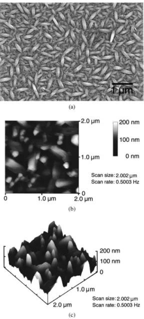
boat temperature of 400 °C, which was regulated by a power supply and a K-type thermocouple. The microstructure was observed by means of field emission gun scanning electron microscopy 共FEGSEM兲, as shown in Fig. 1共a兲. The AlQ3 film is stacked by nanometer-sized rods, which are about 100 nm wide and 0.5–1 m long. The surface morphology was also examined by atomic force microscopy 共AFM兲, as dis-played in Fig. 1共b兲. The roughness of the surface is about 100 nm, as shown in Fig. 1共c兲.
A polarization-modulation near-field scanning optical microscopy 共PM–NSOM兲8,9 was employed to verify the crystallinity of the nanorods. As the combination of conven-tional polarization microscopy and near-field scanning opti-cal microscope provides the image of crystalline domains with a resolution less than 100 nm,10 it is feasible to inves-tigate the nanocrystalline domains of the AlQ3 film. In this work, the incident laser has a wavelength of 400 nm, close to the absorption band of the AlQ3. The incident light was
modulated to form a rotated linearly polarized light. In a crystalline domain, the absorption varies with the direction of linear polarization. Therefore, a dichroic ratio 共R兲 and a phase signal 共兲 can be measured through the polarization-modulation technique. The dichroic ratio共R兲 is defined as8
R⫽I储⫺I⬜
I储⫹I⬜, 共1兲
where I储and I⬜are the transmission light intensities that are parallel and perpendicular to the principal crystalline axis, respectively. The phase signal is the orientation angle where the direction of linearly polarized light coincides with the principal crystalline axis.8The dichroic ratio is related to the degree of crystallinity and the phase image is related to the
a兲Electronic mail: [email protected] b兲Electronic mail: [email protected]
APPLIED PHYSICS LETTERS VOLUME 83, NUMBER 22 1 DECEMBER 2003
4607
alignment direction of the domain. The dichroic and phase images of the AlQ3 crystalline film are shown in Fig. 2.
According to the dichroic image, Fig. 2共a兲, the crystallized regions are clearly found in the bright area. The dichroic ratio has a maximum value of about 0.37. The phase image with a value varying from⫺90° to ⫹90° is displayed in Fig. 2共b兲. Compared to the dichroic image, the phase image re-veals the directions of crystalline domains. The angle is the same in a single domain and is different for each domain. The crystalline film of AlQ3 has also been reported
previously,5 although both films were grown by different mechanisms. Moulin et al.5 fabricated the AlQ3 crystalline
film on an oriented polytetrafluoroethylene substrate at tem-peratures in the range of 50–100 °C. In this work, the crys-talline film was grown on an ITO substrate at⫺196 °C.
To check if the AlQ3 molecules are decomposed during
evaporation, the chemical bondings of the AlQ3 crystalline
film and original powder were examined by Fourier-transform infrared spectrum. Except for the peaks due to CO2 and H2O, all the other absorption peaks between 400
and 2000 cm⫺1 are in good agreement with the reported
results.11The absorption peaks of the crystalline film are the same as those of the AlQ3 powder, indicating that the bond-ing of the molecule is preserved even after evaporation at 400 °C.
The PL spectra of AlQ3 amorphous and crystalline films deposited on silicon substrate were obtained by exciting with a He–Cd laser of a wavelength 325 nm and power 50 mW. The amorphous film of a thickness 1200Å was deposited at 1.33⫻10⫺3 Pa with a disposition rate of 3–5 Å/s controlled by a quartz monitor. It yields a strong and smooth green visible light luminescence ranging from 4500 to 7000 Å with the maximum intensity at about 5380 Å, as shown in Fig. 3共a兲. On the contrary, vibronic evolution of PL spectrum was observed from the AlQ3 crystalline film, as shown in Fig.
3共b兲. In ordered organic molecular solids, the vibronic pro-gression with several separated peaks have been shown pre-viously, but only in the spectrum of AlQ3crystalline sample
measured at 4.2 K.12Here the vibronic progression in the PL spectrum of AlQ3 crystalline film is measured at room
tem-perature. It is reported that the splitting of the peaks is attrib-FIG. 1. Microstructures of the AlQ3 crystalline film:共a兲 FEGSEM image,
共b兲 AFM image, and 共c兲 roughness of surface.
FIG. 2. PM–NSOM images of the AlQ3crystalline film:共a兲 dichroic ratio
image and共b兲 phase image.
FIG. 3. PL spectra of the AlQ3films:共a兲 amorphous and 共b兲 crystalline.
uted to the coupling of vibrations of the individual ligands to the fluorescence transition.13After fitting the vibrational PL spectrum, the locations of individual peaks are positioned at 474, 488, 506, 528, 550, 578, 610, and 646 nm as shown in Fig. 4. The average spacing of these peaks is about 800 cm⫺1, which is larger than 655–700 cm⫺1 reported elsewhere.13
Field emission of polycrystalline diamond film has been observed for many years.14 Recently, AlQ3 nanowires have
been fabricated and shown to exhibit field emission.7 The AlQ3 polycrystalline film reported here is an organic
semi-conductor that shows field emission with a relatively low turn on voltage. The field emission properties were measured with a 50 m gap between the anode and the cathode at a base pressure of 1.0⫻10⫺5Pa. A spherical-shaped platinum probe with an estimated area of 1.6⫻10⫺3 cm2 was used as the anode. The AlQ3 polycrystalline film was deposited on
an ITO coated glass substrate and acted as the cathode. The field emission instrumentation has a sphere-to-plate geom-etry rather than plane-to-plane, because the platinum probe provides precise motion and manipulation inside the high vacuum environment. Therefore, the field emission proper-ties in any region of the film can be measured. The field emission characteristics are presented by the curve of current density J versus applied field E, as shown in Fig. 5共a兲. The turn-on field is 12.0 V/m when the current density reaches 0.01 mA/cm2. The field emission yields a current density of about 0.8 mA/cm2at 22 V/m. The Fowler–Nordheim plot of ln(J/E2) vs 1/E, shown in the inset of Fig. 5共a兲, yields a straight line demonstrating the field emission phenomenon.15 The stability test of the AlQ3 polycrystalline film was
per-formed with an initial current density of about 0.35 mA/cm2 and an applied field of 20 V/m for more than 2000 s, as illustrated in Fig. 5共b兲. The field emission current varied when different region of the film was measured by the plati-num probe. It revealed that the field emission current was strongly dependent on the surface roughness of the film. Ac-cording to the AFM image shown in Fig. 1共c兲, the polycrys-talline film is stacked with nanometer-sized rods and the roughness of the surface depth is about 100 nm. It demon-strates that the electrons may emit from the bumps of the AlQ3 film at high voltages. The effect of surface roughness
on electron emission from polycrystalline diamond films has
been reported,14but the same mechanism for a small molecu-lar organic semiconductor is demonstrated here.
This work was supported by the National Science Coun-cil of ROC under Contract No. NSC-91-2215-E-002-024 and Ministry of Education of ROC under Contract No. A-91-E-FA04-1-4. The authors are grateful to Teng-Fang Kuo and Hong-Jen Lai of Materials Research Laboratory of the Indus-trial Technology Research Institute, Taiwan, ROC, for their help in the measurement of field emission.
1Y. Cao, I. D. Parker, G. Yu, C. Zhang, and A. J. Heeger, Nature共London兲 397, 414共1999兲.
2
C. W. Tang and S. A. VanSlyke, Appl. Phys. Lett. 51, 913共1987兲.
3M. D. Halls and H. B. Schlegel, Chem. Mater. 13, 2632共2001兲. 4K. Naito and A. Miura, J. Phys. Chem. 97, 6240共1993兲.
5J. F. Moulin, M. Brinkmann, A. Thierry, and J. C. Wittmann, Adv. Mater. 共Weinheim, Ger.兲 14, 436 共2002兲.
6J. J. Chiu, W. S. Wang, C. C. Kei, and T. P. Perng, Appl. Phys. Lett. 83,
347共2003兲.
7J. J. Chiu, C. C. Kei, T. P. Perng, and W. S. Wang, Adv. Mater.共Weinheim,
Ger.兲 15, 1361 共2003兲.
8
P. K. Wei and W. S. Fann, J. Microsc. 202, 148共2001兲.
9P. K. Wei, S. Y. Chiu, and W. L. Chang, Rev. Sci. Instrum. 73, 2624 共2002兲.
10E. Betzig and J. K. Trautman, Science 257, 189共1992兲. 11
M. D. Halls and R. Aroca, Can. J. Chem. 76, 1730共1998兲.
12M. Brinkmann, G. Gadret, M. Muccini, C. Taliani, N. Masciocchi, and A.
Sironi, J. Am. Chem. Soc. 122, 5147共2000兲.
13G. P. Kushto, Y. Iizumi, J. Kido, and Z. H. Kafafi, J. Phys. Chem. A 104,
3670共2000兲.
14
N. Koenigsfeld, R. Kalish, A. Cimmino, D. Hoxley, S. Prawer, and I. Yamada, Appl. Phys. Lett. 79, 1288共2001兲.
15V. V. Zhirnov, C. L. Rinne, G. J. Wojak, R. C. Sanwald, and J. J. Hren, J.
Vac. Sci. Technol. B 19, 87共2001兲.
FIG. 4. Vibronic progression of PL spectrum and its curve-fitting.
FIG. 5.共a兲 Field emission of the AlQ3polycrystalline film. The inset shows
the Fowler–Nordheim plot.共b兲 Field emission stability of the AlQ3
poly-crystalline film tested at 20 V/m for more than 2000 s.
4609