Fabrication of sub-100-nm metal-oxide-semiconductor field-effect transistors with
asymmetrical source/drain using I-line double patterning technique
Horng-Chih Lin, Tzu-I Tsai, Tien-Sheng Chao, Min-Feng Jian, and Tiao-Yuan Huang
Citation: Journal of Vacuum Science & Technology B 29, 021007 (2011); doi: 10.1116/1.3551527
View online: http://dx.doi.org/10.1116/1.3551527
View Table of Contents: http://scitation.aip.org/content/avs/journal/jvstb/29/2?ver=pdfcov Published by the AVS: Science & Technology of Materials, Interfaces, and Processing
Articles you may be interested in
Capped carbon hard mask and trimming process: A low-cost and efficient route to nanoscale devices J. Vac. Sci. Technol. B 31, 021603 (2013); 10.1116/1.4789349
Residual-type mask defect printability for extreme ultraviolet lithography J. Vac. Sci. Technol. B 30, 06F501 (2012); 10.1116/1.4756934
Fabrication of complementary metal-oxide-semiconductor integrated nanomechanical devices by ion beam patterning
J. Vac. Sci. Technol. B 27, 2691 (2009); 10.1116/1.3253550
Fabrication of 22 nm half-pitch silicon lines by single-exposure self-aligned spatial-frequency doubling J. Vac. Sci. Technol. B 25, 2224 (2007); 10.1116/1.2801889
Fabrication of 12 nm electrically variable shallow junction metal–oxide–semiconductor field effect transistors on silicon on insulator substrates
Ta Hsueh Road, Hsinchu, Taiwan 300, Republic of China
共Received 24 August 2010; accepted 9 January 2011; published 31 January 2011兲
The authors present a simple double patterning technique with I-line stepper to define nanoscale structures and have successfully fabricated n-channel metal-oxide-semiconductor field-effect transistors 共MOSFETs兲 with sub-100-nm gate length. With this approach, polycrystalline silicon 共poly-Si兲 gate with linewidth down to 80 nm could be formed with good control, which far exceeds the resolution limit of conventional I-line lithography. Moreover, ineffectiveness of end point detection in the second poly-Si gate definition is also addressed. For reliable process control in the second etching step, appropriate mask design is found to be essential. Finally, sub-100-nm MOSFETs with or without halo implemented symmetrically or asymmetrically are fabricated and characterized. © 2011 American Vacuum Society. 关DOI: 10.1116/1.3551527兴
I. INTRODUCTION
Lithography has been playing a pivotal role in semicon-ductor manufacturing since the advent of integrated circuit 共IC兲. Actually the successful evolution of IC technology strongly relies on the advancement of lithography tools and associated processes. To this date, immersion ArF-193 tools have been employed for 32 nm node manufacturing.1 How-ever, this is achieved at the expense of the skyrocketing equipment and process cost. The advanced tools suitable for high-volume manufacturing are usually out of reach in university-based laboratories. As a result most of the experi-mental studies on nanoscale devices carrying out in univer-sities rely on alternative techniques such as photoresist共PR兲 ashing,2,3 e-beam writing,4 and imprinting5 or using bottom-up approach 共e.g., metal-catalytic growth6兲 to form the nanoscale structures.
I-line steppers have been employed for a long time for both manufacturing and research purposes, and the associ-ated lithographic process is very mature and reliable. How-ever, for conventional I-line process the generated PR pattern width is typically 0.3 m or wider. Although nanoscale di-mensions can be achieved by combining with the PR ashing technique,2,3it requires a highly stable asher to ensure good reproducibility and uniformity of critical dimension共CD兲 of the printed patterns. Besides, rounding of the top PR can be another concern for subsequent etching step.3 On the other hand, immersion ArF-193 and deep ultraviolet共DUV兲 lithog-raphy are capable of generating nanoscale patterns. However,
the immersion ArF-193 and DUV tools are outrageously ex-pensive. Accounting for the tool and maintenance cost, most of studies carried out in universities thus opt for e-beam li-thography to generate nanopatterns. Nonetheless, the scheme suffers from a very low throughput as compared with photo-lithography methods.
In this work, we propose a simple method which com-bines both I-line lithographic process and double patterning 共DP兲 technique to address the above issues. As compared with the e-beam direct writing method, I-line process excels in throughput but is much worse in resolution capability which is limited by the optical diffraction phenomenon. On the other hand, DP technique which typically requires twice lithographic and/or etch steps has been proposed to increase the density of devices7,8and has also been demonstrated with the capability of breaking the resolution limit of an optical system.9,10 As a matter of fact, it has been considered as a viable approach for sub-32-nm nodes by integrating with the immersion ArF-193 process.11 Even with the I-line process, generation of structures with nanoscale dimensions is ex-pected if the DP technique is incorporated. In this work we explore such feasibility by successfully fabricating sub-100-nm n-channel metal-oxide-semiconductor field-effect transistors 共n-MOSFETs兲. Additional merit associated with the process demonstrated in this work is the implementation of asymmetrical source/drain共S/D兲 which could increase the flexibility in device design. Such capability is lacking with the aforementioned e-beam and PR ashing techniques. None-theless, an issue encountered in polycrystalline silicon 共poly-Si兲 gate etch step of the present approach is also presented
and discussed. The characteristics of fabricated devices with symmetrical or asymmetrical S/D are analyzed and dis-cussed.
II. DOUBLE PATTERNING METHOD
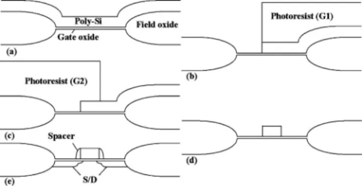
Figure1illustrates the major process steps in the fabrica-tion of n-MOSFETs with the DP technique. For all litho-graphic steps carried out in this work, we used an I-line stepper共Canon FPA-3000i5+兲 to generate PR patterns. First, local oxidation of Si共LOCOS兲 was used for device isolation. Then, after p-well and threshold-voltage共Vth兲 adjustment im-plantations, thermal gate oxide of 3 nm was grown in a N2O ambient, followed by the deposition of a 150 nm in situ phosphorous-doped poly-Si, as shown in Fig. 1共a兲. Subse-quently, DP technique was executed to pattern the poly-Si gate. This procedure employed two masks denoted as G1 and G2 to define the gate electrode, as shown in Fig.2. The two lithographic processes of G1 and G2 were aligned with the preexisting zero-layer alignment mark formed on the wafer. Mask G1 was first applied to generate PR patterns covering portion of the poly-Si, as shown in Fig. 1共b兲, followed by a reactive ion etch共RIE兲 step to remove the uncovered poly-Si. The second lithographic step with mask G2 was then
employed to generate PR patterns which covered portion of the poly-Si layer remaining on the surface of the substrate 关Fig. 1共c兲兴, followed by a RIE step to complete the final poly-Si structure. As can be seen in Fig.2, the most critical portion in the design is the overlapped region of the two gate patterns in the active area which determines the channel length共Lovp兲 of the fabricated device. After the gate
pattern-ing 关Fig.1共d兲兴, the remaining process steps follow the con-ventional flow, namely, source/drain extension implant, side-wall spacer formation, and deep S/D implant关Fig.1共e兲兴.
III. END POINT DETECTION ISSUE
During device fabrication, a major issue related to the ineffectiveness of end point detection 共EPD兲 in the second poly-Si etch step was found. Figure3shows the evolution of optical emission signal intensity during the second poly-Si etch on a test wafer. Normally the end point should be de-tected at around 20 s after the turning on of plasma, but this did not happen and the signal remained stable. Moreover, the signal intensity appeared to be much weaker than that re-corded during the first poly-Si etch. Since the signal intensity is related to the etch by-products,12 this is believed to be related to the layout design of mask G1. In the original ver-sion of G1 mask, over 90% of the blanket poly-Si area is not covered by the PR and is etched off in the first poly-Si etch step, so the end point共defined as the moment when the in-tensity drops to 90% of the peak inin-tensity兲 can be easily detected in the main etch stage of the first etch step. How-ever, with the scanty poly-Si left during the second etch, only a very weak optical signal is detectable, causing the failure of EPD.
Owing to the ultrathin gate oxide, EPD failure may cause the breakthrough of the gate oxide and result in device fail-ure. Figure4illustrates the cross-sectional scanning electron microscopy共SEM兲 image of a MOSFET showing a recess in the Si substrate at the right side of the gate, an indication of the damage induced in the second etching process. When this happens, the devices exhibit very leaky characteristics and are no longer suitable for practical application.
The above issue could be resolved by modifying the lay-out design of the mask G1. This was done by adding dummy
FIG. 1. Major process steps for fabricating n-MOSFETs with the DP method.共a兲 Formation of gate oxide and poly-Si on Si wafer with LOCOS isolation. 共b兲 Generation of first PR pattern 共G1兲, followed by the first poly-Si etching.共c兲 Generation of second PR pattern 共G2兲 after removing the first PR.共d兲 Completion of the poly-Si gate after second poly-Si etching and subsequent PR removal.共e兲 Formation of S/D structure.
FIG. 2. 共Color online兲 Layouts of the first 共G1兲 and second 共G2兲 gate pat-terns for defining the gate pattern on the active region. Gate length共L兲 of the final gate is determined by the overlap region of the two gate patterns.
FIG. 3. Typical optical emissive signal recorded during the main etching stage of the second gate etching with the original mask design. No end point was detected.
Lin et al.: Fabrication of sub-100-nm metal-oxide-semiconductor field-effect transistors
021007-2 021007-2
patterns to the layout of the mask G1 to boost the remaining area of the poly-Si film after the first etching step. These dummy patterns removed in the second etching step could contribute more etch by-products and increase the optical signal for effective EPD. The feasibility of the modified mask design is evidenced by the EPD results recorded during the first and second poly-Si gate etchings shown in Figs.5共a兲 and 5共b兲, respectively. In the two etching steps EPD could both be successfully carried out. To further highlight the
ef-fectiveness of the new layout design, the in-line SEM pic-tures of the poly-Si line after the second etch with original and modified layout are shown in Figs.6共a兲and6共b兲, respec-tively. An obvious etch-induced damage region, correspond-ing to the Si recess region shown in Fig.4, is observed at the right side of the gate in Fig. 6共a兲. In Fig. 6共b兲, with the modified layout, such damage could be completely elimi-nated.
IV. CRITICAL DIMENSION CHECK
In-line SEM was employed to measure the linewidth of patterned poly-Si gates. The results are shown in Fig. 7. Here, the horizontal axis is the nominal designed value de-noted as Lovpand the vertical axis is the actual value after the
gate formation process mentioned in Sec. II, denoted as Lpoly. FIG. 4. 共Color online兲 Cross-sectional SEM view of a MOSFET showing an
etch-induced recess at the right side of the gate. Top illustration is used to help visualize the structure. The recess was formed during the G2 etching stage due to the failure of EPD.
FIG. 5. Optical emissive signal recorded during the main etching stage of the 共a兲 first and 共b兲 second gate etchings with the modified mask design. Suc-cessful EPD is achieved in the two etch steps.
FIG. 6. In-line SEM views of gate patterns on active region etched with共a兲 original and共b兲 modified mask designs. The etch recess phenomenon can be resolved with the modified mask design.
As can be seen in this figure, the dimensions of the printed polygates are close to those of the mask patterns. Figure 8
shows the cumulative plots of the measured poly-Si gates with nominal lengths of 80, 300, and 400 nm, patterned with the DP technique. Also shown in the figure are the results of poly-Si gates with nominal length of 350 nm patterned with conventional I-line technique. In the figure each curve repre-sents measured data obtained from 35 test samples distrib-uted across the test wafer. The results clearly demonstrate the capability of this approach not only to shrink the gate length beyond the resolution limit of single patterning technique 共⬎300 nm兲 but also to achieve a better dimension control as compared with conventional I-line process. Even with a much smaller gate dimension, the distribution in the mea-sured gate width of the DP-patterned lines is obviously tighter than that of the conventional I-line method. Since the feature sizes of G1 and G2 patterns are much larger than the resolution limit of the I-line stepper, the CD variation is strongly dependent on the alignment accuracy of the expo-sure tool. According to the specifications of the employed stepper provided by the vendor, the overlay accuracy共3兲 is about 45 nm. This value is close to the deviation of the measured data共51 nm兲 with the DP technique shown in Figs.
7and8. In other words, the overlay accuracy of the exposure tool sets the limit for the CD control of the present approach. This may result in a noticeable variation in device
character-istics as its dimensions are small. Fortunately, such concern can be relieved with a modification in process steps to tailor the device structure. An example is the implementation of asymmetrical S/D, which is characterized and discussed in Sec. V.
V. DEVICE CHARACTERISTICS
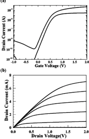
Figures9共a兲and9共b兲show the transfer and output char-acteristics of a MOSFET with L = 100 nm fabricated with the process flow illustrated in Figs.1共a兲–1共e兲. In this case the shallow S/D extensions were formed by implanting As+共10
keV, 1⫻1015 cm−2兲. After forming a 100 nm
tetraethoxysi-lane oxide sidewall spacer, deep S/D junctions were formed by implanting As+ 共20 keV, 5⫻1015 cm−2兲 and then
an-nealed at 1000 °C for 10 s. Good device performance with drain induced barrier lowering 共DIBL兲 of 119 mV/V and subthreshold swing of 80 mV/dec is obtained. These results are comparable to those presented in previous work on de-vices fabricated with DUV共193 nm兲 lithography.13We have also characterized the devices with L = 80 nm and typical transfer characteristics are shown in Fig.10. Figure 11 is a SEM picture showing the cross-sectional image of the de-vice. Obviously, as compared with the results shown in Fig.
9, the device shows significant short-channel effect in terms of high subthreshold leakage and large DIBL. To address this
FIG. 7. Measured poly-Si gate length共Lpoly兲 is shown as a function of nomi-nal gate length共Lovp兲.
FIG. 8. 共Color online兲 Cumulative plots of poly-Si gates patterned with DP method with nominal lengths of 80, 300, and 400 nm and with conventional single patterning with nominal length of 350 nm. Each curve represents the results measured from 35 test structures.
FIG. 9. 共a兲 Transfer characteristics measured at VD= 0.05 and 1.5 V and共b兲 output characteristics of a control device with gate length of 100 nm and width of 10 m measured at VGS− Vt= 0 – 2 V and step= 0.4 V.
Lin et al.: Fabrication of sub-100-nm metal-oxide-semiconductor field-effect transistors
021007-4 021007-4
issue, we have further implemented the halo scheme14in the device fabrication and the results are presented later.
Historically MOSFET fabrication usually adopts sym-metrical S/D structure because of its simplicity and relatively lower cost as compared with the asymmetrical counterparts. In principle, an asymmetrical S/D, having different source and drain doing profiles in terms of doping concentration, junction depth, and even doping type, can offer more free-doms for device performance optimization,15–17 but its for-mation may need additional lithographical and implantation steps in conventional single patterning scheme. In contrast, the DP method lends itself nicely to the implementation of an asymmetrical S/D. For example, we can perform the implan-tation of source- and drain-side extensions individually and specifically after the first 关Fig. 1共b兲兴 and second 关Fig. 1共c兲兴
etch steps of poly-Si gate, respectively, so a greater flexibil-ity in extensions’ profile design can be obtained. Moreover, implementation of one-side halo doping15for controlling the short-channel effects is also feasible with the DP approach. In this regard, we have fabricated and characterized three types of devices. The process flow of these devices is basi-cally the same as that described previously for the devices
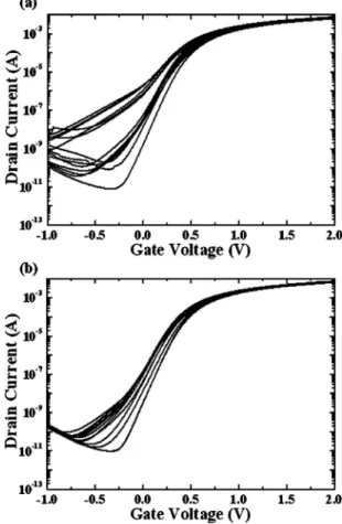
shown in Figs. 9共a兲, 9共b兲, and 10, except the addition of several steps for forming the halo doping wherever neces-sary. One of the three types of devices denoted as “control” has no halo implemented. The devices characterized in Figs.
9共a兲,9共b兲, and10belong to this category. The second type, denoted as “S/D halo,” has halo doping embedded symmetri-cally in both source and drain. The last type denoted as “S halo” has halo doping embedded only in the source side. The former two types are symmetrical, while the last one is asymmetrical in structure. Halo implants were done with BF2+ 共5⫻1012 cm−2/50 keV/45° tilt angle兲. For the
S/D-FIG. 10. Transfer characteristics of a control device with gate length of 80 nm and width of 10 m measured at VD= 0.05 and 1.5 V. As compared with the device characteristics shown in Fig.9共a兲, a much higher subthreshold leakage is observed in the device.
FIG. 11. Cross-sectional SEM image of an 80 nm poly-Si gate formed on active region.
FIG. 12. 共Color online兲 Output characteristics of control, S/D-halo, and S-halo n-MOSFETs with L = 80 nm measured at VGS− Vt= 0 – 2 V and step= 0.4 V.
FIG. 13. Transfer characteristics of共a兲 S/D-halo and 共b兲 S-halo n-MOSFETs with L = 80 nm measured at VD= 0.05 and 1.5 V.
halo split, the halo doping was performed after the extension implant关Fig.1共d兲兴. For the S-halo one, it was done after the first gate etch关Fig.1共b兲兴. Figure12shows and compares the output characteristics of the three types of devices. To evalu-ate the variation in device characteristics, each device shown in the figure represents the results from 15 test devices with nominally identical dimensions and mean performance among its group. As can be seen in the figure, the implemen-tation of the halo doping tends to decrease the current drive. This is reasonable since halo introduces extra substrate dop-ing in the channel and thus the carrier mobility is degraded. Nonetheless, the effectiveness of halo in alleviating the short-channel effects is evidenced by the transfer character-istics shown in Figs.13共a兲and13共b兲for S/D halo and S halo, respectively. In the figures, obviously, the two-sided halo is more effective than the one-sided halo. However, the degra-dation in on current with the introduction of halo is relaxed with the S halo, as shown in Fig.12.
Another important merit of halo is the tightened variation of device characteristics. This can be understood with the transfer characteristics of control and S/D-halo devices shown in Figs.14共a兲and14共b兲, respectively. In Fig.15 de-vices of each type were measured at drain bias 共VD兲
= 1.5 V. Clearly the S/D halo can help to reduce device variation. Similar measurements were also performed on S-halo devices, and the results are shown in Figs.15共a兲and
15共b兲 for forward and reverse modes of operation, respec-tively. Here, forward mode means the normal operation con-dition, while reverse mode is with the drain grounded and the source applied with 1.5 V. The results clearly show that the reverse mode exhibits a tighter distribution of the current-voltage curves, confirming the ability of drain-side halo in preventing the penetration of electric field from the nearby junction into the channel.
Finally, it should be noted that the feature of easily incor-porating asymmetrical S/D with the present DP scheme makes this approach also suitable for fabricating tunneling field-effect transistors 共TFETs兲 which demand source and drain of different doping types in order to form the gated
p-i-n structure.18,19 This can be done by performing the source doping after the first gate etch 关Fig. 1共b兲兴 and the
drain doping with opposite type after the second gate etch. In other words, TFET is an inherently asymmetrical device and usually needs more mask counts than conventional MOSFETs20 to fabricate; it is thus well suited for the DP scheme reported in this work as far as nanoscale gate length is concerned.
VI. CONCLUSIONS
In this work we have successfully demonstrated the gen-eration of sub-100-nm patterns using DP technique with an
FIG. 14. Transfer characteristics of 共a兲 15 control and 共b兲 15 S/D-halo n-MOSFETs with L = 80 nm measured at VD= 1.5 V.
FIG. 15. Transfer characteristics of 15 S-halo n-MOSFETs with L = 80 nm measured at VD= 1.5 V for共a兲 forward mode and 共b兲 reverse mode. Forward mode is measured with the source grounded and the drain is applied with 1.5 V, while reverse mode is with the role of S/D switched.
Lin et al.: Fabrication of sub-100-nm metal-oxide-semiconductor field-effect transistors
021007-6 021007-6
ineffectiveness of EPD in the second gate etching step. This issue was resolved by adding dummy patterns in the layout design of the first gate mask. Another concern is the limit set by the overlay accuracy of the exposure tool. For more pre-cise CD control, tools with improved overlay accuracy are needed. To examine the feasibility of the I-line DP process, 80 nm n-MOSFETs with symmetrical and asymmetrical Ss/Ds were fabricated and characterized. The results clearly indicate the usefulness of the proposed I-line DP technique for nanoscale device fabrication and the effectiveness of the asymmetric S/D for improving the device characteristics. The extra mask thus provides not only greatly enhanced ca-pability in shrinking the device dimensions but also more flexibility in device fabrication.
ACKNOWLEDGMENTS
The authors would like to thank the staff at Nano Facility Center of the NCTU and National Nano Device Laboratories 共NDL兲 for their assistance in device fabrication. This work was supported in part by the National Science Council under Contract No. NSC 98-2221-E-009-160.
1P. Packan et al., Tech. Dig. - Int. Electron Devices Meet. 2009, 659. 2J. Chung, M. Jeng, J. E. Moon, A. T. Wu, T. Y. Chan, P. K. Ko, and C.
8K. M. Monahan, Proceedings of IEEE International Symposium on Semi-conductor Manufacturing共IEEE, New York, 2006兲, p. 126.
9P. Rigolli, C. Turco, U. Iessi, G. Capetti, P. Canestrari, and A. Fradilli, J. Vac. Sci. Technol. B 25, 2461共2007兲.
10K. Ronse, P. Jansen, R. Gronheid, E. Hendrickx, M. Maenhoudt, V. Wiaux, A.-M. Goethals, R. Jonckheere, and G. Vandenberghe, IEEE Trans. Circuits Syst., I: Regul. Pap. 56, 1884共2009兲.
11V. S. Basker et al., Dig. Tech. Pap. - Symp. VLSI Technol., 19共2010兲. 12C. Y. Chang and S. Sze, ULSI Technology 共McGraw-Hill, New York,
1996兲, p. 362.
13H. S. Kim, S. Y. Ong, M. Sarkar, Y. W. Teh, S. M. Pandey, F. Benistant, E. Quek, M. Bhat, and S. Chu, Proceedings of European Solid State Device Research Conference (ESSDERC)共IEEE, New York, 2002兲, p. 319.
14Y. Taur and E. J. Nowak, Tech. Dig. - Int. Electron Devices Meet. 1997, 215.
15T. N. Buti, S. Ogura, N. Rovedo, and K. Tobimatsu, IEEE Trans. Electron Devices 38, 1757共1991兲.
16K.-Y. Huang, P.-C. Wang, M.-C. Hung, Y.-S. Jean, T.-H. Yeh, and Y.-H. Lin, Proceedings of IEEE Radio Frequency Integrated Circuits Sympo-sium共IEEE, New York, 2008兲, p. 263.
17K. Narasimhulu, D. K. Sharma, and V. R. Rao, IEEE Trans. Electron Devices 50, 2481共2003兲.
18O. M. Nayfeh, C. N. Chleirigh, J. Hennessy, L. Gomez, J. L. Hoyt, and D. A. Antoniadis, IEEE Electron Device Lett. 29, 1074共2008兲.
19W. Y. Choi, B.-G. Park, J. D. Lee, and T.-J. King Liu, IEEE Electron Device Lett. 28, 743共2007兲.
20T. Nirschl et al., Proceedings of International Conference on Microelec-tronic Test Structures共IEEE, New York, 2005兲, p. 43.