Effect of compressive stress on nickel-induced lateral crystallization of amorphous
silicon thin
films
S.Y. Huang, H.L. Lin, C.G. Chao, T.F. Liu
⁎
Department of Materials Science and Engineering, National Chiao Tung University, Taiwan, ROC
a b s t r a c t
a r t i c l e i n f o
Article history:
Received 11 February 2010
Received in revised form 10 November 2011 Accepted 17 November 2011
Available online 25 November 2011 Keywords:
Metal-induced lateral crystallization Nickel
Amorphous silicon Polycrystalline silicon Glass substrate
Secondary ion mass spectroscopy Raman spectroscopy
The present study describes a method enabling the metal-induced lateral crystallization (MILC) of amorphous silicon (a-Si) films. Glass substrates coated with a-Si films were contacted with ground nickel sheets under compressive stresses ranging from 3.7 to 265.8 MPa at 550 °C for 1 h. Subsequently, the nickel sheet and stress were removed and the specimens were annealed at 550 °C for 1 to 4 h. The experimental results indicate that the extent of MILC decreased when the preliminary compressive stress was increased, while all specimens exhibited the same rate of lateral crystallization during annealing. The present study indicates that, by applying an appropriate compressive stress (~ 4 MPa), an effective method to reduce the residual Ni content in polycrystalline silicon (poly-Si) can be obtained.
© 2011 Published by Elsevier B.V.
1. Introduction
Polycrystalline silicon (poly-Si) thinfilm transistors (TFTs) show better electrical performance than amorphous silicon (a-Si) TFTs. Two of the most popular methods currently used to fabricate poly-Si TFTs are solid phase crystallization (SPC) and excimer laser annealing. Although the SPC method is having the advantage of low cost, it is, however, hampered by the needs of an elevated temperature above 600 °C and long processing time [1–3]. Consequently, excimer laser annealing is currently the preferred method for the fabrication of low-temperature poly-Si TFTs. The excimer laser annealing, nonetheless, is not cost-effective, albeit that large high quality crystallites have been obtained by this method. Recently, an alternative method termed as metal-induced lateral crystallization (MILC) of a-Si has attracted much attention, because it can yield high quality poly-Si crystallites at temperatures much lower than 600 °C. Among various metals, nickel-induced lateral crystallization (NiLC) TFTs have been the focus of attention, owing to the superior device properties demonstrated in NiLC TFTs as compared to those prepared using other metals[4,5]. However, a problem with NiLC TFTs is that large amount of residual Ni has been found to induce unexpectedly larger leakage currents than those measured in conventional MILC TFTs[6]. Three methods have been proposed to solve the problem. Thefirst method is the get-tering technique practiced by the Sharp Company to reduce the
amount of residual Ni in poly-Si and, hence, the leakage current[7]. In the second method, a poly-Si wafer is bonded to a base plate and subjected to MILC. The base plate effectively captures the residual Ni, giving rise to a significant reduction of Ni in the poly-Si[8,9]. The third method is called the metal imprint technology[10]. In that, a chip array coated with a metal layer is pressed onto the a-Si to promote nucleation in subsequent solid-phase crystallization. However, all of these methods involve rather complex manufacturing processes and are inevitably with relatively higher operation cost. Therefore, the development of alternative methods capable of reducing the amount of residual Ni effectively with low operation cost is of vital importance. In the present study, we demonstrate that, by directly contacting a Ni sheet with the a-Sifilm and applying an appropriate compressive stress, not only the phenomenon of NiLC is evidently observed but also the amount of the residual Ni in poly-Si can be effectively reduced. The present method, thus, may have potential significance in the display industry.
2. Experimental details
For obtaining high thermal conductivity[11], a 200-nm-thick SiNx
film was deposited on a Corning 1737 °F glass substrate as the buffer layer. Subsequently, a 200-nm-thick a-Sifilm was deposited on the buffer layer, and the sample was then cut into test specimens with a typical size of 10× 10 mm. The test specimens were cleaned with the standard RCA cleaning process. Pure (99.99%) nickel sheets with a size of 12 × 12 × 1 mm were ground by using #80, #400, and #2000 abrasive papers, respectively. A custom made device used to apply compressive
⁎ Corresponding author.
E-mail address:tfl[email protected](T.F. Liu).
0040-6090/$– see front matter © 2011 Published by Elsevier B.V. doi:10.1016/j.tsf.2011.11.041
Contents lists available atSciVerse ScienceDirect
Thin Solid Films
stress on the specimens is schematically shown inFig. 1. The device consists of two stainless steel discs with three screw holes, two graphite spacers facing each other for clamping the specimen, and molybdenum rods and nuts. The test specimens were brought into contact with the abrasion-treated nickel sheets of varying roughness and were clamped in the above mentioned device for applying compressive stress. The compressive load applied on the specimens was adjusted to within the range between 1 and 2 MPa (10–20 kgw/cm2), with a
spring-loaded screw located at the end of the specimen holder. Then, the entire assembly with the pressurized specimen was placed in a furnace with an Ar atmosphere at 550 °C for 1 h. This process is referred to as“the seeding step.” After the seeding step, the test specimens were removed from the holder for examining their microstructure. In the annealing step, the specimens were sealed in vacuum tubes and annealed at 550 °C for 1 to 4 h. Atomic force microscopy (AFM, Digital Instruments, Model no.LFM-2) was operated in contact mode using scan window sizes of 100 × 100μm with resonance frequency of 13 kHz and n+
silicon tip; field-emission scanning electron microscopy (FE-SEM, JOEL-6500 F) was operated in 15 keV, 40μA; energy-dispersive spec-trometry (EDS, Oxford Link ISIS200) was operated in 15 keV, 40μA; Raman spectrometry (Jobin Yvon HR-800) used Ar+ laser source
(λ=514.5 nm). These instruments were carried out to investigate the microstructure of the specimens. The time-of-flight secondary ion mass spectrometry (ToF-SIMS) used for this study is a CAMECA IMS 4f spectrometer. Depth profiles were measured using an 8 keV O2+sputter
beam with a 57° incidence to the sample surface giving a 100 nA target current over a 250 × 250μm area.
3. Results and discussion 3.1. Seeding step
AFM analyses indicated that after being ground by the #80, #400, and #2000 abrasive papers, the nickel sheets had a surface average roughness of 527 nm, 125 nm, and 37 nm, respectively. A typical 2-D AFM image is shown inFig. 2and through thisfigure the roughness of Ni sheet could be obtained by AFM analysis. The average roughness (Ra) value was also defined as the mean value of the surface relative
to the center plane using
Ra¼ 1 LxLy XLy 0 XLy 0 f xð; yÞ j jdxdy
where f(x, y) is the surface relative to the center plane and Lxand Lyare
the dimensions of the surface.
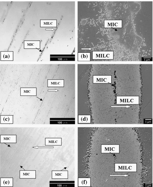
Fig. 3(a), (c), and (e) shows the optical micrographs of the surface morphology of the specimens after the seeding step. It is evident from the micrographs that the crystallized area comprises two distinct regions, namely, the black areas and the gray areas surrounding the black areas. During the seeding step, the specimens and Ni sheets were brought into contact with each other. Thus, actual contacts were expected to occur at the small peaks randomly distributed on the surface of the abrasion-treated Ni sheets. Under the seeding conditions (550 °C), Ni may interact with the a-Si at the contacting points to form silicide (NiSix). Subsequently, crystallization of Si occurred via the
epitaxial growth of Si crystal on the {111} faces of the octahedral NiSi2
precipitates because of an extremely small lattice mismatch (0.4%) [12]. The black spots seen inFig. 3(a), (c), and (e), presumably are the areas directly in contact with Ni, whereby the metal-induced crystalli-zation (MIC) is taking place. In order to further confirm the above con-jectures, the thickness of the NiSixcompound (black area) and the Ni
content in the NiSixcompound for specimens treated under various
compressive loadings were analyzed by AFM and EDS, respectively. The results are summarized as shown inTable 1. It is evident from Table 1that the nickel content is as high as 76.2 at.% in the marked MIC areas for specimen treated with the highest compressive stress (specimen A), suggesting that the NiSixcompound may include Ni2Si,
NiSi, and NiSi2.
The crystalline seeds resulting from MIC then grew laterally into the regions of a-Si that were not originally in contact with Ni and formed large crystallized areas; this process is referred to as MILC. It is noted that while the size of the MIC areas (black areas) increased with increasing compressive stress, the opposite tendency was observed for the MILC areas (gray areas). We note here that although the nominal applied stress varies only in the range of 1–2 MPa, the actual compressive stress, however, has to take the real contact area into account. The contact peak area was measured using the image analysis software, Image Pro. For example, the contact area calculated by the software for the surface shown inFig. 3(a) was approximately 0.75% of the total area. At an applied stress of 2 MPa, the average compressive stress was estimated to be approximately 266 MPa. The re-sults for the six specimens examined in the present study are also listed inTable 1. The table indicates that both the thickness of the NiSix
com-pound and the Ni content increased with increasing compressive stress. After the AFM analyses, the test specimens were treated by a Secco etchant in order to reveal the features of the MILC areas in more detail. Fig. 3(b), (d), and (f) shows the SEM micrographs taken from the spec-imens ofFig. 3(a), (c), and (e), respectively. In these Figures, it is seen that the specimen subjected to the highest compressive stress shows the least degree of MILC, while for specimens subjected to lower com-pressive stresses (such as E and F) obvious MILC is observed. According to Shewman's report[12], the stress can significantly affect the diffusion coefficient of materials. Thus, in the present Ni-induced lateral
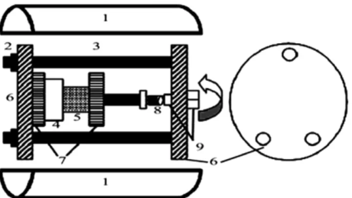
Fig.1. Schematic of the custom-made device used for applying compressive stress on spec-imens. The numbered segments in thefigure respectively represent furnace (1), Mo nut (2), Mo rod (3), Ni sheet (4), specimen (5), stainless steel disc (6), graphite spacer (7), spring (8), and screw (9).
crystallization event, the process is believed to occur sequentially with the following three steps:
2Niþ Si→Ni2Si…… ð1Þ
Ni2Siþ Si→2NiSi…: ð2Þ
NiSiþ Si→NiSi2…… ð3Þ
Hayzelden argued that reaction(3)is a diffusion control process [13]. Furthermore, it was reported by Cheng et al.[14]that increasing compressive stress tends to decrease the vacancy density in materials, resulting in a reduced diffusion coefficient. Therefore, it is plausible to suggest that the low degree of MILC observed in specimen A (266 MPa) and specimen B (133 MPa) might be due primarily to the relatively higher compressive stresses applied. On the other hand, when the applied compressive stress is less than 38 MPa, noticeable MILC can be obtained, as displayed in specimens C, D, E, and F.
3.2. Annealing step
According to the relationship between the length of the MILC and annealing time during the annealing step, the estimated rate of MILC was approximately 3.3μm/h for all specimens. This result is consistent with the previously published data[15]. It is clear that although the compressive stress can affect the formation of NiSi2 and may even
retard the initiation of MILC, the growth rate of the MILC is, however, al-most the same no matter how much NiSi2existing under free stress at
550 °C. This is further indicative that without the effect of applied stress the growth of the MILC crystallites is mainly controlled by diffusion.
Fig. 3. Optical micrographs and corresponding SEM images of specimens A, E, and F after the seeding step (a)–(b) specimen A (266 MPa), (c)–(d) specimen E (8 MPa), and (e)–(f) specimen F (4 MPa).
Table 1
Thickness of NiSixcompound and Ni content for specimens after the seeding step.
Specimen (compressive stress; MPa) Thickness of NiSix compound (nm) Ni content (at.%) A (265.8) 185.9 76.2 B (132.9) 92.4 37.0 C (38.2) 30.6 13.7 D (19.1) 19.3 11.5 E (7.4) 12.2 3.2 F (3.7) 8.7 0.3
3.3. Raman spectrum analysis
The Raman spectrum analyses were carried out to identify crystalli-zation of the silicon thinfilm and to decide the amount of crystallization quantitatively. The characteristic peak of the silicon Raman spectrum is situated between 480 and 500 cm−1 for amorphous silicon and between 510 and 520 cm−1for silicon nano-crystallites. The character-istic Raman peak of crystalline silicon at 517.11 cm−1 is clearly observed in this study. The estimated size of the crystalline silicon is about 50 nm, which is consistent with the diameter of the needle-like grains displayed inFig. 3. The quantity of the crystallized silicon that resulted from both MIC and MILC processes can be estimated by the integrated area under the peak.Fig. 4(a) and (b) illustrates the Raman spectra of specimens A (266 MPa) and F (4 MPa) with various anneal-ing times. The blank curve represents that the raw specimen which did not make contact with Ni sheet. A0 and F0 curves represent the results of the specimens that were only treated by the seeding step. A1, A2, A4 and F1, F2, F4 curves represent the results for the specimens that have been further subjected the annealing step for 1, 2, and 4 h, respectively. Both blank curves inFig. 4(a) and (b) show that no crystal-line silicon was formed at 550 °C if the specimens did not make contact with the Ni sheet. Both A0 and F0 curves reveal that the silicon crystal-lization had occurred after the seeding step. InFig. 4(a) and (b), it is found that the area under the peak of curve A0 is much smaller than that of the curve F0. This result is consistent with the observations in Fig. 3, where the suppressed MIC event has been attributed to the decreased vacancy density induced by the large applied compressive stress. In addition, the peak intensity of crystalline silicon increased with increasing annealing time in the annealing step, indicating that the MILC proceeds continuously with prolonged annealing time.
3.4. SIMS analysis
FromTable 1, it is clear that after the seeding step, the EDS results indicate that the nickel content in the MIC regions of the test specimens increases with the increasing compressive stress. Therefore, it would be interesting to check how the annealing step affects the nickel content in the newly formed poly-Si crystallites. We chose specimen F, which had the lowest nickel content, to detect the residual nickel content by using the ToF-SIMS analysis. The result is shown inFig. 5. It is seen in this Fig-ure that the SIMS intensity drops rapidly from the surface and remains a largely constant plateau within ~40–120 nm beneath the surface. Since the initial NiSixseeding layer was only about 9 nm-thick for this case
(Table 1), the current result, thus, implies that during MILC process the residual nickel content inside the crystallized poly-Si can be signif-icantly lower than 0.3 at.% which is the initial content of the MIC region determined EDS. In any case, although there are still many issues, such as the detailed mechanism of MILC, remaining to be clarified, the present study has, nevertheless, demonstrated that by applying an appropriate compressive stress it is possible to obtain effective MILC at relatively lower temperatures with minimal amount of residual nickel content in the crystallized poly-Si.
4. Conclusions
In summary, we have studied the effect of compressive stress on nickel-induced lateral crystallization of amorphous silicon thinfilm. After the seeding step (by direct mechanical contact under pressure and high temperature), both the thickness of NiSixcompound (MIC
area) and Ni content were found to increase with the increasing com-pressive stress. However, the applied comcom-pressive stress appeared to have an opposite effect on inducing MILC. The appearance of the charac-teristic Raman peak at 517.11 cm−1evidently indicated the formation of crystalline silicon during the seeding step. During the annealing step for MILC, a constant growth rate of 3.3μm/h was observed for all specimens investigated in this study. The present study demonstrates that by applying an appropriate compressive stress it is possible to ob-tain effective MILC at relatively lower temperatures with minimal amount of residual nickel content in the crystallized poly-Si.
Acknowledgment
The authors acknowledge thefinancial support provided by Wintek Corporation for this research. The research was supported in part by National Science Council of Taiwan.
Fig. 4. Raman spectra of crystalline Si (a) specimen A (266 MPa) and (b) specimen F (4 MPa) annealed at 550 °C for various times. A0 and F0 curves represent the specimens only treated by the seeding step. A1, A2, A4 and F1, F2, F4 curves represent the specimens that have been further subjected the annealing step for 1, 2, and 4 h, respectively.
References
[1] A. Nakamura, F. Emoto, E. Fujii, A. Yamamoto, Y. Uemoto, K. Senda, G. Kano, J. Appl. Phys. 66 (1989) 4248.
[2] A. Nakamura, F. Emoto, E. Fujii, Y. Uemoto, A. Yamamoto, K. Senda, G. Kano, Jpn. J. Appl. Phys. 27 (1988) 2408.
[3] J.H. Kim, J.Y. Lee, K.S. Nam, J. Appl. Phys. 77 (1995) 95. [4] S.W. Lee, S.K. Joo, IEEE Electron. Device Lett. 17 (1996) 160.
[5] C.J. Lee, J.B. Lee, Y.C. Chung, D.K. Choi, Jpn. J. Appl. Phys. 39 (2000) 6191. [6] T.H. Ihn, et al., SID Dig., May, 1997, p. 188.
[7] T. Mizuki, J.S. Matsuda, Y. Nakamura, J. Takagi, T. Yoshida, IEEE Trans. Electron Dev. 51 (2004) 204.
[8] C.M. Hu, Y.S. Wu, C.C. Lin, IEEE Electron. Dev. Lett. 28 (11) (2007) 1000.
[9] P.C. Liu, C.Y. Hou, Y.S. Wu, Thin Solid Films 478 (2005) 280.
[10] K. Makihira, M. Yoshii, T. Asano, Electronics and Communications in Japan, 2003 86 (No. 5) (2003) 45 Part 2.
[11] J.H. Park, S.M. Han, S.G. Park, M.K. Han, M.Y. Shin, Phys. Scr. T126 (2006) 85. [12] P. Shewman, Diffusion in Solids (Minerals, Metals & Materials Society), Pennsylvania.
2nd ED, 1989, p. 85.
[13] C. Hayzelden, J.L. Batstone, J. Appl. Phys. 73 (12) (1993) 8279.
[14] L.W. Cheng, H.M. Lo, S.L. Cheng, L.J. Chen, C.J. Tsai, Mater. Sci. Eng., A 409 (2005) 217.
[15] C.F. Cheng, T.C. Leung, M.C. Poon, C.W. Kok, M. Chan, Electron Dev. 51 (12) (2004) 2205.