This content has been downloaded from IOPscience. Please scroll down to see the full text.
Download details:
IP Address: 140.113.38.11
This content was downloaded on 26/04/2014 at 09:46
Please note that terms and conditions apply.
InGaN self-assembled quantum dots grown by metal–organic chemical vapour deposition with
growth interruption
View the table of contents for this issue, or go to the journal homepage for more
2006 Nanotechnology 17 1713
(http://iopscience.iop.org/0957-4484/17/6/028)
Nanotechnology 17 (2006) 1713–1716 doi:10.1088/0957-4484/17/6/028
InGaN self-assembled quantum dots
grown by metal–organic chemical vapour
deposition with growth interruption
H H Yao, T C Lu, G S Huang, C Y Chen, W D Liang, H C Kuo and
S C Wang
1Department of Photonics and Institute of Electro-Optical Engineering, National Chiao Tung University, Ta Hsueh Road, Hsinchu 30050, Taiwan, Republic of China
E-mail:[email protected]
Received 24 October 2005, in final form 25 January 2006
Published 27 February 2006
Online at
stacks.iop.org/Nano/17/1713
Abstract
Self-assembled InGaN quantum dots (QDs) were grown by metal–organic
chemical vapour deposition with growth interruption at low V/III ratio and
low growth temperature on sapphire substrates. The effects of the
interruption time on the morphological and optical properties of InGaN QDs
were studied. The results show that the growth interruption can modify the
dimension and distribution of InGaN QDs, and cause the QD emission
wavelength to blue shift with increasing interruption time. A density of
InGaN QDs of about 4
.5 × 10
10cm
−2with an average lateral size of 11.5 nm
and an average height of 1.6 nm can be obtained by using a growth
interruption time of 60 s.
(Some figures in this article are in colour only in the electronic version)
1. Introduction
Wide bandgap gallium nitride (GaN) and other group III nitride based semiconductors have been successfully employed to realize short wavelength light emitting diodes and laser diodes (LDs) [1–3]. Additionally, due to quantum confinement effects, fabrication and studies of GaN based nanostructures have recently attracted a great deal of interest for potential applications in electronic and optoelectronic devices. The quantum confined nanostructures and quantum dot (QD) structures are low dimension confinement structures and have many unique physical characteristics. For example, the application of QD structure in LDs has been known to lead to lower threshold currents due to the enhancement of excitonic effects in the quantum dots [4]. For GaN based materials, a report suggested that III nitride QD structures can reduce the effect of defect density on the device performance [5]. There are various techniques reported for the growth of InGaN QDs structures by metal–organic chemical vapour deposition (MOCVD). These include the use of antisurfactant to change the surface free energy of epilayers [6], control of
1 Author to whom any correspondence should be addressed.
the growth thickness and temperature [7] as well as using the growth interruption technique [8–11]. Among these, the growth interruption approach facilitates elastic relaxation resulting in the formation of 3D island structure [8] because the adatoms can relax to energetically favourable positions and approach thermodynamic equilibrium during the growth interruption [9]. However, effects of different interruption times on the growth of InGaN QDs have not been reported. In this paper, we report the growth of self-assembled InGaN QDs by MOCVD at low V/III ratio and low growth temperature on sapphire substrates and the results of the investigation of the effect of the interruption time on the morphological and optical properties of the InGaN QDs grown.
2. Experiment
All samples were grown using a low pressure vertical-type MOCVD system (EMCORE D75). A 30 nm GaN nucleation layer was grown first at 500◦C on a (0001)-oriented sapphire substrate and this was followed by a GaN buffer layer grown at 1110◦C under H2 ambient gas. During the growth of the
H H Yao et al (b) Height (nm) Distance(nm) Distance(nm) (a) (c) Height (nm) 0.0 0.2 0.4 0.6 0.8 1.0 1.2 1.4 1.6 0.0 0.2 0.4 0.6 0.8 1.0 0 200 400 600 800 1000 0 15 30 45 60 75 90
Figure 1. (a) A typical AFM 1µm × 1 µm image of sample B with tint= 30 s, (b) a section analysis along the dashed line in (a), (c) the
shape profile of a single InGaN QD structure.
0 10 20 30 40 50 0 20 40 60 80 100 0 20 40 60 80 100 120 0 50 100 150 200 0 5 10 15 20 25 30 35 40 45 50 0 20 40 60 80 100 120 0 10 20 30 40 50 60 Sample A Sample B Sample C (a) (c) (d) (f) Counts Counts (b) (e)
Lateral Size (nm) Height (nm)
0 1 2 3 4 5 6
Figure 2. Histograms of the dot lateral size and height distribution. (a), (b), (c) are the lateral size distributions for samples A, B and C,
respectively. (d), (e), (f) are the height distributions for samples A, B and C, respectively.
68.4µmol min−1and NH3was used as a group V source with
a flow rate of 3 l min−1, corresponding to a V/III ratio of about
2000. The surface morphology of the GaN buffer layer is very flat with an average deviation Ra = 0.14 nm measured by
an external atomic forced microscopy (AFM) system since a previous report had shown that the flat template surface was important for fabricating self-assembled InGaN QDs without using antisurfactant [7]. After the GaN buffer layer was grown, the growth temperature was reduced to 660◦C to grow an InGaN layer and the growth time of all samples was fixed at 30 s. Unlike in the standard InGaN quantum well growth, the growth temperature was reduced and the growth time was increased to facilitate the InGaN quantum dot growth [7]. During the growth of InGaN, the flow rates of TMG and trimethylindium were 4.92 and 4.80µmol min−1, respectively, and the flow rate of NH3 was 2 l min−1, corresponding to a
low V/III ratio of about 8300 in comparison to the normal V/III ratio of 30 000 in the InGaN quantum well growth. During the growth of the InGaN film, N2 was used as the
ambient gas with a flow rate of 5 l min−1. After the InGaN growth was completed, a growth interruption was introduced for these samples with different interruption times (tint) of 30,
60 and 120 s for samples A, B and C, respectively. The surface morphologies of these samples were examined by AFM and the AFM data were analysed by a scanning probe image processor (SPIP) to gather the geometric statistics of InGaN QDs. The optical characteristics of these samples were investigated with photoluminescence (PL) using a commercial microscope system.
3. Results and discussion
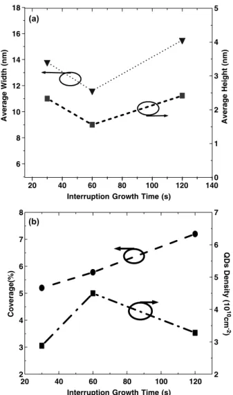
The topographic images of three InGaN QDs samples were measured by AFM and all images showed small island morphology. Figure1(a) is a typical AFM scanned result over an area of a 1 µm square of sample B with the interruption time of 60 s. A section analysis along the dashed line in figure 1(a) is shown in figure 1(b), and the dense QD distribution can be observed. Figure 1(c) clearly shows the shape profile of a single InGaN QD structure with the lateral size and height of about 30 and 0.8 nm, respectively. In addition, the surface roughness average deviation decreases from Ra = 0.26 to Ra =0.21 nm on increasingtintfrom 30
to 120 s. This indicates that the growth interruption at 660◦C could influence the surface morphologies. In order to gather geometric statistics for InGaN QDs, SPIP was used to analyse the AFM data for InGaN QDs structures. The lateral size and height histograms associated with each sample are shown in figure 2. The standard deviations of QD height is 1.19, 0.78 and 0.91 nm for samples A, B and C, respectively. The results indicate that growth interruption may be beneficial for producing uniform distribution of InGaN QD size. Figure3(a) shows the averaged height and lateral size of the samples with various interruption times. The mean sizes (lateral size, height) of samples A, B and C are (14 nm, 2.4 nm), (11.5 nm, 1.6 nm), (15 nm, 2.5 nm), respectively. The InGaN QDs reduced first then increased their dimensions as the interruption time increased. Figure3(b) shows the dependences of the QD coverage, which describes how much QD area is occupied on the surface above the wetting layer, and the QD density on the interruption time. The QD coverage increases from 5.2% to 7.2% on increasing tint from 30 to 120 s. On the
other hand, the QD densities are 2.88×10¹⁰, 4.50×10¹⁰
and 3.28×1010cm−2for samples A, B and C, respectively.
Average Height (nm)
Average Width (nm)
Interruption Growth Time (s) 6 8 10 12 14 16 18 20 40 60 80 100 120
Interruption Growth Time (s)
20 40 60 80 100 120 140 0 1 2 3 4 5 QDs Density (10 10 cm -2 ) Coverage(%) 2 3 4 5 6 7 2 3 4 5 6 8 7 (a) (b)
Figure 3. (a) Average lateral size and height dependence on the
interruption time and (b) dependence of the density and the coverage of InGaN QDs on the interruption time.
Sample B withtint=60 s has the largest QD density. The QD
coverage always increases as the interruption time increases implying that the sample surface could have an adatom surface diffusion effect during the process of growth interruption [12]. During the growth interruption period 30 s < tint < 60 s,
the increase in dot density could be caused by the adatom diffusion from wetting layers to generate new dot structures, while the decrease in average dot size could be due to the adatom desorption from ‘old’ dot structures. For the growth interruption period 60 s< tint<120 s, the dot density decrease
and average size increase could be mainly due to the adatom surface diffusion between the InGaN QDs, which leads to the enlargement of the larger islands by combination of smaller ones due to the Ostwald ripening [13].
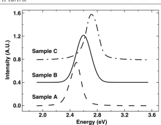
Figure4shows the PL spectra of InGaN QDs for various interruption times from 30 to 120 s at room temperature (RT). A He–Cd laser was used as the excitation source in the PL measurement. The PL emission peaks are 2.49, 2.60 and 2.72 eV, and PL linewidths are 170, 210 and 180 meV for samples A, B and C, respectively. The RT PL of the InGaN QDs samples shows a blue-shift trend as the interruption time
H H Yao et al Sample C Sample B Sample A Intensity (A.U.) 2.0 2.4 2.8 3.2 3.6 Energy (eV) 0.0 0.4 0.8 1.2 1.6
Figure 4. Photoluminescence spectra of samples A, B and C at room
temperature under the excitation power of 20 mW.
increases from 30 to 120 s. However, the average heights of the InGaN QDs samples are 2.4, 1.6 and 2.5 nm for samples A, B and C, respectively, as shown in figure 3(a), indicating that the sizes of the InGaN QDs are not always decreased with increasing interruption time; the blue shift of the PL emission peak may be caused by the reduction of the In composition in the InGaN QDs during the growth interruption. A similar effect was also reported for the InGaAs QDs [14]. The decrease of the In composition in the InGaN QDs suggests that the desorption rate of In atoms could be larger than that of Ga atoms at 660◦C. In addition, the PL linewidth exhibited by sample B was obviously larger than that for samples A and C. Since QD size reduction would increase the fluctuation of the effective size distribution leading to an increase of the PL inhomogeneous broadening [15], the relatively small QD size of sample B should be responsible for the large PL linewidth despite the dispersion of QD dimensions.
4. Conclusion
Self-assembled InGaN QDs structures were grown on sapphire substrates by MOCVD with growth interruption. The flat GaN layer on the sapphire substrate with an average deviationRa=
0.14 nm of roughness over an area of a 1µm square was used as the template for growing InGaN QDs at a low V/III ratio (∼8300), low growth temperature (660◦C) conditions and with various interruption times. The InGaN QDs grown at tint= 60 s
have a density of about 4.5×1010cm−2with an average lateral
size of 11.5 nm, and an average height of 1.6 nm was obtained. The interruption time effects on the morphological and optical properties of the InGaN QDs suggest that the desorption effect during the growth interruption could decrease the dimensions of the InGaN QDs structure; the surface diffusion effect during the growth interruption could increase the QD coverage on the surface above the wetting layer, and extend the emission wavelength to the short wavelength region with increase of the interruption time. By appropriately adjusting the interruption time, uniformly distributed InGaN QDs with small dimensions can be obtained and should usable for applications in GaN based light emitting devices.
Acknowledgments
This work was supported in part by the National Science Council of the Republic of China (ROC) in Taiwan under contract Nos NSC 93-2120-M-009-006 and NSC 93-2115-E009-068.
References
[1] Nakamura S, Senoh M, Iwasa N and Nagahama S 1995 Japan.
J. Appl. Phys.34 L797
[2] Nakamura S, Mokia T and Senoh M 1994 Appl. Phys. Lett.
64 1687
[3] Yu C C, Chu C F, Tsai J Y, Huang H W, Hsueh T H, Lin C F and Wang S C 2002 Japan. J. Appl. Phys.41 L910
[4] Uenoyama T 1995 Phys. Rev. B51 10228
[5] Li J, Ye Z and Nasser N M 2003 Physica E16 244
[6] Hirayama H, Tanaka S, Ramvall P and Aoyagi Y 1998 Appl.
Phys. Lett.72 1736
[7] Tachibana K, Someya T and Arakawa Y 1999 Appl. Phys. Lett.
74 383
[8] Damilano B, Grandjean N, Semond F, Massies J and Leroux M 1999 Appl. Phys. Lett.75 962
[9] Meixner M, Kunert R and Scholl E 2003 Phys. Rev. B
67 195301
[10] Oliver R A, Briggs G A D, Kappers M J, Humphreys C J, Yasin S, Rice J H, Smith J D and Taylor R A 2003 Appl.
Phys. Lett.83 755
[11] Ji L-W, Su Y-K, Chang S-J, Wu L-W, Fang T-H, Xue Q-K, Lai W-C and Chiou Y-Z 2003 Mater. Lett.57 4218
[12] Min B D, Kim Y, Kim E K, Min S-K and Park M J 1998 Phys.
Rev. B57 11879
[13] Convertino A, Cerri L, Leo G and Viticoli S 2004 J. Cryst.
Growth261 458
[14] Leon R, Yong K, Jagadish C, Gal M, Zou J and Cockayne D J H 1996 Appl. Phys. Lett.69 1888
[15] Peter R, Philippe R, Shintaro N, Yoshinobu A and Satoru T 2000 J. Appl. Phys.87 3883