This content has been downloaded from IOPscience. Please scroll down to see the full text.
Download details:
IP Address: 140.113.38.11
This content was downloaded on 26/04/2014 at 09:47
Please note that terms and conditions apply.
Electrical properties of resistance switching V-doped SrZrO3 films on textured LaNiO3 bottom
electrodes
View the table of contents for this issue, or go to the journal homepage for more 2006 J. Phys. D: Appl. Phys. 39 1156
(http://iopscience.iop.org/0022-3727/39/6/022)
INSTITUTE OFPHYSICSPUBLISHING JOURNAL OFPHYSICSD: APPLIEDPHYSICS
J. Phys. D: Appl. Phys. 39 (2006) 1156–1160 doi:10.1088/0022-3727/39/6/022
Electrical properties of resistance
switching V-doped SrZrO
3
films on
textured LaNiO
3
bottom electrodes
Chih-Yi Liu
1, Arthur Wang
2, Wen-Yueh Jang
2and
Tseung-Yuen Tseng
1,31Department of Electronics Engineering and Institute of Electronics, National Chiao-Tung
University, Hsinchu 300, Taiwan, Republic of China
2Winbond Electronics Corporation, Hsinchu 300, Taiwan, Republic of China
3Department of Materials and Mineral Resources Engineering, National Taipei University of
Technology, Taipei 106, Taiwan, Republic of China E-mail:[email protected]
Received 18 November 2005, in final form 16 January 2006 Published 3 March 2006
Online atstacks.iop.org/JPhysD/39/1156
Abstract
Sputter-deposited V-doped SrZrO3(SZO) films were deposited on textured
LaNiO3(LNO) bottom electrodes to investigate the resistance switching
properties and reliabilities. The microstructures of the SZO and LNO films were characterized by x-ray diffraction. The resistance of the Al/V-doped SZO/LNO sandwich structures can be reversibly switched by operating with dc bias voltages or voltage pulses. The device with [100] orientated SZO film had better resistance switching properties and the resistance ratio was more than 1000. The effect of thermal treatment on resistance switching properties was investigated and different behaviour of the two leakage-states was found. Finally, the reliability of the device was also investigated. The device with the properties of reversible resistance switching and non-destructive readout is suitable for nonvolatile memory application.
1. Introduction
Nonvolatile memory (NVM) has recently become an important part of the semiconductor industry due to the popularity of portable equipment. The requirements for a high performance NVM are that it should have the properties of reversible switching, non-destructive readout, low operation voltage, long retention time, high endurance, high operation speed, low power consumption, small size and low cost [1]. Many new devices have been proposed for NVM applications [1–5]. Resistive random access memory (RRAM) is one of the promising candidates for the next generation NVM. The RRAM has the superior properties of reversible switching, long retention time, multilevel switching, simple structure and small size [6]. Recently, perovskite oxide films have attracted much interest in the investigation of the resistive memory effect [7–10]. The resistance of RRAM can be switched between high and low values by operating with dc bias voltages or voltage pulses. In this paper, the sputtering
deposition technique was employed to form the metal/V-doped SrZrO3(SZO)-based insulator/metal (MIM) sandwich
structure. LaNiO3(LNO) films with the advantages of low
cost and low process temperature were fabricated as bottom electrodes to study the effect of the textured bottom electrodes on the resistance switching properties. The effect of thermal treatment on the resistance switching properties of the SZO film was also investigated. Finally, the reliability of the SZO-based RRAM was studied.
2. Experimental
The 4 inch boron-doped (100) silicon wafers were cleaned by the standard Radio Corporation of America (RCA) cleaning process. After cleaning, a 200 nm thick SiO2 layer was
thermally grown on silicon substrates by a furnace to isolate the leakage current from the silicon substrate. Then a 60 nm thick LNO conducting film was grown at 300◦C on a SiO2/Si
Electrical properties of resistance switching V-doped SrZrO3films
2 theta (degree)
20 30 40 50 60Intensity
(arb.
u
n
it
)
0 200 400 600 800 LN O( 20 0) S Z O( 20 0) L N O( 110 ) LN O( 20 0) S Z O( 10 0) LNO/SiO2/Si SZO/LNO/SiO2/Si (a)2 theta (degree)
20 30 40 50 60In
te
ns
it
y
(ar
b.
un
it
)
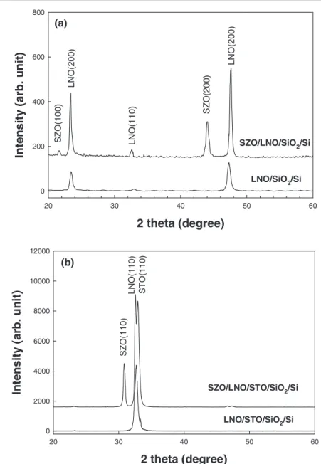
0 2000 4000 6000 8000 10000 12000 LNO/STO/SiO2/Si SZO/LNO/STO/SiO2/Si SZ O (1 1 0 ) LNO( 110) S T O(11 0) (b)Figure 1. XRD patterns of (a) LNO/SiO2/Si and SZO/LNO/SiO2/Si structure, (b) LNO/STO/SiO2/Si and SZO/LNO/STO/SiO2/Si structure.
second approach, a 50 nm thick SrTiO3 (STO) buffer layer
was deposited at 550◦C on a SiO2/Si substrate and then a
60 nm LNO film was deposited at 300◦C to form a [110] orientated bottom electrode. After that the 90 nm thick 0.2% V-doped SZO films were deposited on the above two different textured electrodes at 450◦C with the same deposition time as the insulator layers. All LNO, STO and SZO thin films were prepared by radio-frequency (rf) magnetron sputtering. Finally, a 300 nm thick Al top electrode was deposited by a thermal evaporator to form the MIM sandwich structures for electrical measurement. The area of top electrodes patterned by a metal mask was 4.9× 10⁻⁴cm2. The crystallized orientation was examined by x-ray diffraction (XRD, Rigaku x-ray diffractometer). On the basis of the XRD data, the average grain size was determined using Scherrer’s formula. An Agilent 4155C semiconductor parameter analyser was used to record the current–voltage (I –V ) characteristics and the Agilent 81110A pulse generator was used to generate voltage pulses to change the resistance of the MIM device.
3. Results and discussion
Figure1depicts the XRD patterns of the two different textured LNO bottom electrodes and the SZO films on these electrodes. The 300◦C deposited LNO film on the SiO2/Si substrate had
[100] preferred orientation, as shown in figure1(a). Obviously, a highly orientated LNO film can be successfully grown at such a low process temperature. Figure 1(a) also depicts that the [100] orientated SZO film was deposited on this LNO/SiO2/Si substrate. However, it is difficult to deposit
a [110] orientated LNO film directly on a SiO2/Si substrate
by the sputtering deposition technique. As a second bottom electrode, a [110] orientated STO film was grown on the SiO2/Si substrate at 550◦C as a template layer and then
a LNO film was deposited on the STO/SiO2/Si substrate
at 300◦C. As a result, the [110] orientated LNO bottom electrode was successfully obtained (figure 1(b)). Finally, the [110] orientated SZO film was successfully grown on the LNO/STO/SiO2/Si substrate (figure 1(b)). Figure 2 shows
C-Y Liu et al Bias Voltage (V) -20 -15 -10 -5 0 5 10 15 20 Le a k a g e C ur re nt Densit y (A/c m 2 ) 10-6 10-5 10-4 10-3 10-2 10-1 100 101 [100] orientated device [110] orientated device Bias Voltage (V) -20 -15 -10 -5 0 5 10 15 20 Rat io 100 101 102 103 high leakage-state low leakage-state
Figure 2. Plots of leakage current density versus bias voltage of the [100] orientated device and the [110] orientated device. The inset is the plot of resistance ratio versus bias voltage of the [100] orientated device.
the plots of leakage current density versus bias voltage of the V-doped SZO-based MIM devices with [100] and [110] orientated SZO films, respectively. Before starting any resistance switching, the I –V characteristics of the [100] orientated device have the lowest leakage current density, that is, the original state (shown in figure4). While the applied voltage in the negative direction was large enough to start the first resistance switching, the I –V characteristics were rapidly changed to follow the curve of the high leakage-state. After that, while the applied voltage in the positive direction was large enough, the I –V characteristics were rapidly changed to follow the curve of the low leakage-state. The sequence can be repeated as described in figure2; the I –V characteristics were switched between high state and low leakage-state and were never switched back to the original leakage-state. The leakage-states can be maintained without power supply, which can be used as memory applications. The resistance ratio of these two leakage-states decreases with the increasing bias voltage in both directions (inset of figure 2), which is due to the different conduction mechanisms of the two leakage-states [11]. The resistance ratio is more than 3 orders of magnitude under low bias voltage and about 100 at 5 V. As can be seen in figure2, the switching voltages are 8 V in the positive direction and−13 V in the negative direction, respectively. The switching voltage should relate to the crystallinity of the SZO film. Furthermore, the asymmetric switching voltages may be due to the asymmetric interfaces of the SZO film with the top and bottom electrodes. The resistance switching for the [110] orientated device is similar to that for the [100] orientated device, but it has a smaller resistance ratio. Besides, the I –V characteristics of the [110] orientated device were less stable in comparison with those of the [100] orientated device. Therefore, the [100] orientated device is more suitable than the [110] orientated device for resistance switching applications. Before the occurrence of any resistance switching, the leakage current density of the [100] orientated device was less than that of the [110] orientated device. From the XRD of figure1 and Scherrer’s formula, one can know that the average grain sizes of the [110] orientated SZO film are larger than those of
the [100] orientated SZO film. Although the [110] orientated SZO film had better crystallinity than the [100] orientated SZO film, the [100] orientated device had better resistance switching property. Therefore, the resistance switching properties should be mainly influenced by film orientation. Figure3shows the relation of leakage current density versus time for the [100] orientated device with and without the thermal treatment read 5 times at 1.2 V as varied with different voltage pulses. The thermal treatment was performed by a rapid thermal annealing (RTA) system at 650◦C in O2 ambient for 1 min. After a
+20 V, 500 µs pulse was applied on the top electrode of the [100] orientated device, the leakage current density of the high leakage-state was changed to that of the low leakage-state. After a−20 V, 500 µs pulse was applied, the leakage current density of the low leakage-state was changed to that of the high state. The resistance ratio of the two leakage-states is more than 3 orders of magnitude. The write–read– erase–read sequence can be repeated and the leakage-state would not be altered by read bias voltages. Therefore, a device with the properties of reversible switching by voltage pulses and non-destructive readout is indeed demonstrated. The device with thermal treatment had similar resistance switching behaviour, but the resistance ratio decreased. Compared with the leakage current density of the device without thermal treatment, the leakage current density of the high state remains almost the same whereas that of the low leakage-state increases. However, its static I –V characteristics are almost the same with those of the [100] orientated device without thermal treatment except that the leakage current densities of high and low leakage-states increase a little. Such a phenomenon would be due to the different conduction mechanisms of the two leakage-states. It was reported in our previous study [11] that the leakage current density of the high leakage-state obeyed Ohmic mechanisms and that of the low leakage-state followed the Frenkel–Poole emission. For pulse operation, the leakage current densities are sensitive to pulse width [1]. The charges and traps of the SZO film would be rearranged after a pulse operation, which leads to the variation
Electrical properties of resistance switching V-doped SrZrO3films Time (sec) 0 10 20 30 40 50 Leaka ge Cu rren t Dens it y (A/cm 2 ) 10-6 10-5 10-4 10-3 10-2 10-1 100 as-deposited after RTA 650oC Vp= 20 V Wp= 500µµµµsec low leakage-state high leakage-state positive voltage negative voltage
Figure 3. The influence of thermal treatment on the resistance switching property of the [100] orientated devices.
Stress Time (sec)
0 5000 10000 15000 20000 Leakage C u rrent De n s ity @ 5V (A/cm 2 ) 10-11 10-10 10-9 10-8 10-7 10-6 10-5 10-4 10-3 10-2 10-1 high leakage-state low leakage-state original-state
Figure 4. Plots of leakage current density versus stress time for different leakage-states.
in the leakage current density of the low leakage-state. The resistance ratio of the device with thermal treatment becomes about two orders of magnitude, which is attributed to an increase in the leakage current density of the low-leakage state. Figure4shows the plot of the leakage current density stressed at 5 V versus stress time, indicating that leakage current densities of all leakage-states would not be varied by a constant voltage stress. The larger current density of the original-state occurs at the beginning, then decreases to reach the equilibrium current density after a short period of time, which is a relaxation behaviour. The leakage current density of the leakage-states stressed under negative bias voltage was also not varied (not shown). For the resistance switching, the positive bias voltage tends to change the leakage-states to a low leakage-state while the negative bias voltage tends to change the states to a high state. The leakage-states are not changed to another leakage-state by a dc bias stressing voltage less than the switching voltage, which means
the device has a non-destructive readout property and stores the information for a long time. Furthermore, the device was not degraded after stressing for a long time, indicating that the device had good electrical properties. Figure5shows the retention behaviour of the [100] orientated device. Although the retention behaviour of the RRAM is not well-known at high temperature, thermal acceleration testing was still used to avoid tedious measurement. For the device with a low leakage-state, after being heated at 150◦C for 1.5 h its I –V characteristics obviously decreased. However, the device with a high leakage-state after the same thermal treatment remained almost the same. After being heated at 200◦C for 1.5 h, the I –V characteristics of the device with the low leakage-state decreased to close to that of the original leakage-state. After being heated at 200◦C for 1.5 h, the I –V characteristics of the device with the high leakage-state decreased. At higher heating temperature such as 250◦C, the I –V characteristics of both states reverted to those of the original state. After all 1159
C-Y Liu et al Bias Voltage (V) 0 1 2 3 4 5 L e akag e C urre n t D e n s it y (A/ cm 2 ) 10-12 10-11 10-10 10-9 10-8 10-7 10-6 10-5 10-4 10-3 10-2 10-1 100 high leakage-state low leakage-state original-state
low leakage-state after 150o
C 1.5 h high leakage-state after 200oC 1.5 h
Figure 5. Retention behaviour of the [100] orientated device for different leakage-states.
the leakage-states had reverted back to the original state, the device could still be operated as described in figure2. The retention time of the high leakage-state is about 1.5 h at 250◦C and that of the low leakage-state is about 1.5 h at 150◦C. The above phenomena mean that the original-state is the most stable leakage-state and the L-state is the most unstable leakage-state. From the previous investigation [11], the switching time from the high leakage-state to the low leakage-state is much longer than that from the low leakage-state to the high leakage-state. The difference in the switching time implies different stability of the two leakage-states, which is consistent with the retention behaviour.
4. Conclusions
In conclusion, the SZO-based MIM structures were fabricated by a sputter deposition technique to investigate the resistance switching properties. The [100] orientated device had better resistance switching properties than the [110] orientated device. The reversible resistance switching can be successfully operated with dc bias voltages or voltage pulses. The device was stressed by a constant voltage to demonstrate the non-destructive readout and good electrical properties. The retention behaviour of the high leakage-state and the low leakage-state was different, implying different switching mechanisms.
Acknowledgments
The authors thank the National Science Council of R.O.C. under Project No NSC 93-2215-E009-048 and the Winbond Electronics Corporation Taiwan, for their financial support.
References
[1] Zhuang W W et al 2002 IEDM Technical Digest (IEEE) p 193 [2] Lai S 2003 IEDM Technical Digest (IEEE) p 255
[3] Tseng T Y 2001 Extended Abstracts of 1st Int. Meeting on
Ferroelectric Random Access Memories (Gotemba, Japan)
p 62
[4] Baek I G et al 2003 IEDM Technical Digest (IEEE) p 831 [5] Wang Y K, Huang C H, Tseng T Y and Lin P 2004 J.
Electrochem. Soc. 151 F87
[6] Sezi R, Walter A, Engl R, Maltenberger A, Schumann J, Kund M and Dehm C 2003 IEDM Technical Digest (IEEE) p 259
[7] Beck A, Bednorz J G, Gerber Ch, Rossel C and Widmer D 2000 Appl. Phys. Lett. 77 139
[8] Rossel C, Meijer G I, Bremaud D and Widmer D 2001 J. Appl.
Phys. 90 2892
[9] Aoyama K, Waku K, Asanuma A, Uesu Y and Katsufuji T 2004 Appl. Phys. Lett. 85 1208
[10] Baikalov A, Wang Y Q, Shen B, Lornz B, Tsui S, Sun Y Y, Xue Y Y and Chu C W 2003 Appl. Phys. Lett. 83 957 [11] Liu C Y, Wu P H, Wang A, Jang W Y, Young J C, Chiu K Y
![Figure 2. Plots of leakage current density versus bias voltage of the [100] orientated device and the [110] orientated device](https://thumb-ap.123doks.com/thumbv2/9libinfo/7606887.129670/4.892.206.804.121.422/figure-plots-leakage-current-density-voltage-orientated-orientated.webp)

![Figure 5. Retention behaviour of the [100] orientated device for different leakage-states.](https://thumb-ap.123doks.com/thumbv2/9libinfo/7606887.129670/6.892.231.661.128.433/figure-retention-behaviour-orientated-device-different-leakage-states.webp)
