行政院國家科學委員會專題研究計畫 成果報告
電化學法合成奈米結構氧化鎳複合電極及其在電致色變與
電化學電容特性之研究
研究成果報告(精簡版)
計 畫 類 別 : 個別型 計 畫 編 號 : NSC 96-2221-E-151-027- 執 行 期 間 : 96 年 08 月 01 日至 97 年 07 月 31 日 執 行 單 位 : 國立高雄應用科技大學化學工程與材料工程系 計 畫 主 持 人 : 吳茂松 計畫參與人員: 碩士班研究生-兼任助理人員:楊忠憲 碩士班研究生-兼任助理人員:黃佑安 處 理 方 式 : 本計畫可公開查詢中 華 民 國 97 年 09 月 08 日
行政院國家科學委員會補助專題研究計畫
▓ 成 果 報 告
□期中進度報告
電化學法合成奈米結構氧化鎳複合電極及其在電致色變與電化學電
容特性之研究
計畫類別:■ 個別型計畫
□ 整合型計畫
計畫編號:NSC 96-2221-E-151-027-
執行期間:96 年 08 月 01 日至 97 年 07 月 31 日
計畫主持人:吳茂松
共同主持人:
計畫參與人員:楊忠憲、黃佑安
成果報告類型(依經費核定清單規定繳交):■精簡報告
□完整報告
本成果報告包括以下應繳交之附件:
□赴國外出差或研習心得報告一份
□赴大陸地區出差或研習心得報告一份
□出席國際學術會議心得報告及發表之論文各一份
□國際合作研究計畫國外研究報告書一份
處理方式:除產學合作研究計畫、提升產業技術及人才培育研究計畫、
列管計畫及下列情形者外,得立即公開查詢
□涉及專利或其他智慧財產權,□一年□二年後可公開查詢
執行單位:國立高雄應用科技大學化學工程與材料工程系
中
華
民
國
97 年
09
月
08 日
附件一1
電化學法合成奈米結構氧化鎳複合電極及其在電致色變與電化學電
容特性之研究
Electrochromic and electrochemical capacitive properties of nanostructured nickel oxide composite electrode synthesized by electrochemical deposition
計畫編號:NSC 96-2221-E-151-027 執行期限:96年08月01日 至 97年07月31日
主持人:吳茂松 國立高雄應用科技大學化學工程與材料工程系
1.Abstract
Nanostructured nickel oxide film is synthesized directly onto a transparent and conducting indium tin oxide coated glass substrate by electrochemically anodic deposition from an aqueous solution. The deposited nickel oxide film has an intercrossing nanoflake and highly porous morphology. X-ray diffraction peaks of the film resemble closely to the cubic NiO structure. The deposited film oxidized/reduced electrochemically at 0.36V and 0.25V versus a saturated Ag/AgCl electrode respectively, which corresponds to the reversible changes in coloration and bleaching. The difference in optical response (transmittance), T, at wavelength 550nm between the colored state and bleached state can reach as high as 80%.
Keywords: nickel oxide, electrochromic, porous electrode, nanostructured materials, and electrodeposition.
2. Introduction
Electrochromic materials have attracted attention in recent years because they show reversible optical changes upon intercalation/de-intercalation of the ions or protons, in which the transfer is controlled by an outer voltage source. When the unique optical property of the electrochromic materials is combined with a transparent conducting glass such as an indium tin oxide
(ITO), the electrochromic component may be applied onto architecture windows, known as the smart windows. Generally electrochromic materials are categorized into organic and inorganic, in which the inorganic transition metal oxides such as WO3,1-6 NiO,5-8 MnO2,9,10 and MoO311 are the most widely studied. Within the transition metal oxides, nickel hydroxides and nickel oxides receive scholars’attentions for they are anodic colour formation (the color changes from transparent to brownish-black); and when they are paired up with WO3of cathodic colour formation, the resultant electrochromic component is called the complementary electrode.12,13 There exist many synthesizing methods for nickel oxides, such as sputter,14-18 sol-gel,19,20spin coating,21 vacuum evaporation,22 and anodic deposition.23,24 Among these synthetic methods, electrochemical deposition technique has one advantage over the others: weight and thickness of the nickel oxide film may be easily controlled by controlling the current, bath composition, and bath temperature. However, electrode composed of nanoparticle is difficult to fabricate by the traditional slurry coating method, because nanoparticles have poor dispersibility in slurry (composed of solvent, nanoparticles, polymer binder, and conducting agent, etc.). Thus, it is more advantageous to have the electrode fabricated by the direct electrochemical
deposition of nanostructured nickel oxide onto the substrates at room temperature without any template and/or catalyst. In this study, electrochemically anodic deposition is conducted to synthesize nano-scaled electrochromic nickel oxide on ITO coated glass substrate, and to investigate its morphology, structure, electrochemical and optical properties.
3. Experimental
In the anodic deposition for nickel oxide, electrolyte was a mixture of 0.13M NiSO46H2O, 0.13M Na2SO4, and 0.1M NaOAc; in which NaOAc was the buffer solution, so to keep the electrolyte pH between 6.5 and 7.5 during the entire deposition process.25 The nickel oxy-hydroxide film is deposited by oxidation of Ni2+ to Ni3+ and precipitates on the electrode surface, the overall reaction can be schematically represented as25 2 e OH 3 e 2 Ni(OH) NiO(OH) Ni Ni
ITO coated glass substrate was the working electrode, platinum was the counter electrode, and saturated calomel electrode (SCE) was the reference electrode. The transparent conducting glass ITO was cut into pieces of 14 cm2
, soaked in acetone and ultrasonic vibrated for 20 minutes to wash away any contaminants off the surface. De-ionized water was then used to rinse the ITO in ultrasonic vibration for another 15 minutes. To control the reaction area, every ITO sample was taped to leave an exposed surface area of 11 cm2
. A pre-process was applied to ensure the uniformity and adhesion of the deposited nickel oxide: conduct a 2 mA cm-2 current through each ITO sample in 1M NaOH for 30 seconds for anodic oxidation. During deposition, a constant current of 0.25mA cm-2 was applied for 1 hour. The
resultant nickel oxide film was rinsed with de-ionized water, and annealed for 1 hour at 300oC.
Structure of the nickel oxide film was determined by a glance angle X-ray
diffractometer (GAXRD, Rigaku
D/MAX2500), range 20~80°, scan rate 3° per minute. The surface morphology was observed by a high-resolution scanning electron microscope (Hitachi, S-4700I), operating voltage 15kV. For electrochemical studies, cyclic voltammetry (CV, Keithley 2420) was used in a system of 1M KOH electrolyte, platinum being the counter electrode, and Ag/AgCl being the reference electrode. The scan rate was 10 mV s-1 from -0.2V to 0.6V. Optical studies were carried out with an ultraviolet-visible spectrometer (UV-VIS, Perkin elmer lambda 35), in which the above mentioned system was incorporated to study the in situ spectral response.
4. Results and discussion
Figure 1a is the surface morphology of the electrochemically anodic deposited nickel oxide film after annealing at 300oC. The film is porous and of nano-scaled, the interconnecting network is made up of flaky nickel oxides of thickness 15~20 nm. Cross-section of the film (Fig. 1b) shows that the film is approximately 180 nm thick and porous. A highly porous structure provides a large specific surface area for electrolyte access, therefore, nanostructured nickel oxide film with interconnected nanoflakes may improve electrochromic behavior. Nanostructured nickel oxides are important in electrochromics because they have high surface area, fast redox reactions, and shortened diffusion path in solid phase; electrochromic behavior is, therefore, enhanced by the material’s nanostructure.
3
Figure 2 shows the crystalline structure of the deposited nickel oxide film after annealing at 300oC using a GAXDR. In addition to the peaks for ITO, three more diffraction peaks locate at 37.3° (111), 62.9° (220), and 75.4o (311) are cubic nickel oxide with lattice parameters of a = 4.1771 Å and the space group Fm3m (225) (nickel oxide, JCPDS 47-1049). The mean grain size of the deposited nickel oxide has been calculated using Scherrer’s equation with diffraction peak at 2=37.3o: D=0.9/(cos), where is the X-ray wavelength, is the full width at half maximum (FWHM), and is the Bragg angle. The calculated grain size is about 2.8 nm.
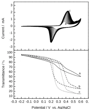
Cyclic voltammogram of the deposited nickel oxide film in 1M KOH aqueous electrolyte is shown in Fig. 3a (scan rate 10 mV s-1). For the first few cycles, oxidation/reduction current peaks fall at 0.36V and 0.25V respectively. As the cycle increases, the current peaks start to move outwards. The peak amplitudes, representing the current values, also increase as cycle increases, then finally stabilize. Fig. 3b, the optical transmittance of the deposited nickel oxide film at wavelength 550 nm, shows that the transmittance changes as the CV cycle increases. At 5th cycle, coloration transmittance (Tc) by oxidation decreases to about 50%; at the 20th cycle, only 25% is left; and when cycle reaches 40 where the transmittance finally stabilizes, Tc decreases to approximately 14%. Of all the CV scan, the deposited nickel oxide film has a constant transmittance in bleached state (Tb), the variation is less than 94%. The difference in transmittance between the colored state and bleached state (T% = Tb-Tc) is approximately 80%. The difference in
transmittance for the sputter,14 pulsed laser deposition (PLD),26 chemical precipitation,27 and sol-gel19 were reported as 40, 48, 53.9, and 38 %, respectively. The intercrossing nanoflake (network) configuration provides much more paths for electron conduction, and the flake-like structure shortens proton diffusion paths within the bulk of solid nickel oxide. In addition, the porous structure benefits electrolyte penetration and provides larger surface area for charge-transfer reactions. Therefore, the optical and electrochemical results of the deposited nickel oxide film are improved.
Figure 4 shows the optical response for the deposited nickel oxide film at colored and bleached states at difference wavelength (300 ~900 nm). Curves a, b, and c are all at bleached states; curve a shows the nickel oxide film right after annealing, curve b shows the nickel oxide film being continuously oxidized with a constant voltage of -0.2V, curve c shows the nickel oxide film being oxidized at -0.2V for 60 seconds then rest for 5 seconds. The three curves are almost identical. When comparing curve b and c, the drop in curve c after voltage shut-off is slight yet pronounced. As the voltage is kept constant (curve b), the transmittance at bleached state at 550 nm reaches as high as 95%; but as the voltage is shut-off for 5 seconds (curve c), the transmittance value drops to 90% or below.
In the coloration state (curves d and e), curve d shows the nickel oxide film being oxidized at 0.5V for 60 seconds then rest for 5 seconds, curve e shows the nickel oxide film being continuously oxidized with a constant voltage of 0.5V. When the two curves are compared, the transmittance does not drop after voltage shut-off (curve d); the
transmittance at bleached state at 550 nm has little variation of 15%.
5. Conclusion
In summary, the nickel oxide film synthesized by electrochemically anodic deposition has cubic NiO crystalline structure after heat annealing at 300oC. The film morphology shows porous and nano-scaled interconnecting network, and the film must be activated electrochemically to achieve the best electrochromic properties. The difference in transmittance (T%) between the colored state and bleached state may reach as high as 80%.
References
1. S. H. Lee, H. M. Cheong, J. G. Zhang, A. Mascarenhas, D. K. Benson, and S. K. Deb, Appl. Phys. Lett. 74, 242 (1999). 2. S. H. Lee, H. M. Cheong, C. E. Tracy, A.
Mascarenhas, J. R. Pitts, G. Jorgensen, and S. K. Deb, Appl. Phys. Lett. 76, 3908 (2000).
3. E. A. Meulenkamp, J. Electrochem. Soc. 144, 1664 (1997).
4. A. Guerfi, R. W. Paunter, and L. H. Dao, J. Electrochem. Soc. 142, 3457 (1995). 5. E. Avendano, L. Berggren, G. A.
Niklasson, C. G. Granqvist, and A. Azens, Thin Solid Films 496, 30 (2006). 6. G. A. Niklasson and C. G. Granqvist, J.
Mater. Chem. 17, 127 (2007).
7. M. Chigane and M. Ishikawa, J. Electrochem. Soc. 141, 3439 (1994). 8. M. Chigane, M. Ishikawa, and H. Inoue,
Solar Energy Mater. Sol. Cells 64, 65 (2000).
9. M. C. Bernard, A. H. Goff, and B. V. Thi, J. Electrochem. Soc. 140, 3065 (1993). 10. M. Chiganez and M. Ishikawa, J.
Electrochem. Soc. 147, 2246 (2000). 11. K. Hinokuma, A. Kishimoto, and T.
Kudo, J. Electrochem. Soc. 141, 879 (1994).
12. S. Passerini, B. Scrosati, A. Gorenstein, A. M. Andersson, and C. G. Granqvist, J. Electrochem. Soc. 136, 3394 (1989). 13. S. Passerini, A. Gorenstein, and B.
Scrosati, J. Electrochem. Soc. 137, 3297 (1990).
14. F. F. Ferreira, M. H. Tabacniks, M. C. A. Fantini, I. C. Faria, and A. Gorenstein, Solid State Ionics 86-88, 971 (1996). 15. E. Avendano, A. Azens, J. Isidorsson, R.
Karmhag, G. A. Niklasson, and C. G. Granqvist, Solid State Ionics 165, 169 (2003).
16. Y. Abe, S. H. Lee, E. O. Zayim, C. E. Tracy, J. R. Pitts, and S. K. Deba, Electrochem. Solid-State Lett. 9, G17 (2006).
17. Y. Abe, S. H. Lee, C. E. Tracy, J. R. Pitts, and S. K. Deba, Electrochem. Solid-State Lett. 9, J31 (2006).
18. C. R. Magan, D. R. Acosta , A. I. Martinez, and J. M. Ortega, Solar Energy 80, 161 (2006).
19. P. K. Sharma, M. C. A. Fantini, and A. Gorenstein, Solid State Ionics 113-115, 457 (1998).
20. R. C. Korosec, P. Bukovec, B. Pihlar, A. S. Vuk, B. Orel, and G. Drazic, Solid State Ionics 165, 191 (2003).
21. Y. Sato, M. Ando, and K. Murai, Solid State Ionics 113-115, 443 (1998).
22. J. Velevska and M. Ristova, Solar Energy Mater. Sol. Cells 73, 131 (2002). 23. S. A. Mahmoud, S. A. Aly, M.
Abdel-Rahman, and K. Abdel-Hady, Physica B 293, 125 (2000).
24. K. Nakaoka, J. Ueyama, and K. Ogura, J. Electroanal. Chem. 571, 93 (2004). 25. D. Tench and L. F. Warren, J.
Electrochem. Soc. 130, 871 (1983). 26. I. Bouessay, A. Rougier, P. Poizot, J.
Moscovici, A. Michalowicz, and J. M. Tarascon, Electrochimica Acta 50, 3737 (2005).
27. W. F. Chen, S. Y. Wu , and Y. F. Ferng, Materials Letters 60, 790 (2006).
5
Figures
Fig.1 (a) Surface morphology and (b) cross-section of the electrochemically anodic deposited nickel oxide film after annealing at 300
o C. 20 30 40 50 60 70 80 (311) In te n s it y / a .u . 2/ degree (111) (220)
Fig. 2 XRD pattern of the deposited nickel oxide film. -0.3 -0.2 -0.1 0.0 0.1 0.2 0.3 0.4 0.5 0.6 0.7 10 20 30 40 50 60 70 80 90 100 c b T ra n s m it ta n c e / Potential / V vs. Ag/AgCl a -3 -2 -1 0 1 2 3 c a C u rr e n t / m A
Fig. 3 Cyclic voltammogram of the deposited
nickel oxide film in 1M KOH aqueous electrolyte.
300 400 500 600 700 800 900 0 10 20 30 40 50 60 70 80 90 100 110 colored film a b c d e T ra n s m it ta n c e / Wavelength / nm bleached film
Fig. 4 Optical response for the deposited nickel oxide film at colored and bleached states at difference wavelength (300 ~900 nm). 附註說明:本計畫原申請為三年期,但核定通 過為一年期,因此成果報告內容為執行期間內 所產出之成果。