國 立 交 通 大 學
電信工程學系
碩士論文
超寬頻通訊脈波產生器之設計
The Design of Pulse Generator for Impulse Radio
Ultra-Wideband Communication
研 究
生:林文筆 (Wun-Bi Lin)
指導教授:陳富強 博士 (Dr. Fu-Chiarng Chen)
超寬頻通訊脈波產生器之設計
The Design of Pulse Generator for Impulse Radio
Ultra-Wideband Communication
研 究 生 : 林文筆 Student : Wun-Bi Lin
指導教授
: 陳富強 博士 Advisor : Dr. Fu-Chiarng Chen
國 立 交 通 大 學
電 信 工 程 學 系 碩 士 班
碩 士 論 文
A Thesis
Submitted to Department of Communication Engineering
College of Electrical and Computer Engineering
National Chiao Tung University
in partial Fulfillment of the Requirements
for the Degree of
Master of Science
In
Communication Engineering
September 2007
Hsinchu, Taiwan, Republic of China
超寬頻通訊脈波產生器之設計
研究生:林文筆 指導教授:陳富強 博士
國立交通大學 電信工程學系碩士班
摘要
本論文為應用於超寬頻脈衝通訊系統之脈波產生器的設計,主要以兩種不同 的技巧來實現出脈波高度可調的單輪脈波,一個使用集總元件製作在 PCB 板 上,另一個則利用台積電的CMOS 0.18μm 製程來實作晶片,其可調性和製作也 都不同。 目前脈波產生器的研究中,以脈波的高度可調性、對稱性和低漣波為最重 要,再者由於晶片中的製程變異或是需應用於不同的情況,因此目前的脈波產生 器研究皆以此目標邁進。本論文提出兩個脈波高度可調的脈波產生器,主要觀念 在於利用 RLC 二階暫態來產生脈波,並利用過阻尼響應來降低脈波尾端的漣波, 從模擬與量測中可驗證此特性。The Design of Pulse Generator for Ultra-Wideband
Communication
Student: Wun-Bi Lin Advisor: Dr. Fu-Chiarng Chen
Department of Communication Engineering
National Chiao Tung University
Abstract
In this thesis, we propose two novel pulse generators for Impulse Radio Ultra-Wideband (IR-UWB) system. The adjustable pulse generators are realized by using two different skills. The first pulse generator is fabricated on PCB utilizing lump elements. On the other hand, the second pulse generator is simulated with TSMC 0.18μm CMOS technology.
The adjustable amplitude range, symmetry and low ringing of the monocycle pulse are important to judge the performance of the pulse generator. Furthermore, the pulse generator should avoid the process variation and be suitable for different requirements. In this thesis, we propose two pulse generators whose pulse amplitude is adjustable. These pulse generators use the second-order transient circuit at over-damping mode to generate the adjustable monocycle pulse with good symmetry and low ringing in the simulation and measurement.
Acknowledgements
誌 謝
本論文能夠順利完成,首先要誠摯的感謝指導教授 陳富強老師,在研 究的過程中提供寶貴的意見和方向,教導我所需的研究態度與解決問題的 能力。老師平時待人寬厚、親切與學生互動良好,不僅在學業上更在做人 處事上時常給予我不一樣的建議。再來也要感謝這兩年內,電信所授課老 師們,有他們也才能夠讓我有更加充實的基本理論,也才能夠順利的把研 究與論文完成。 兩年裡的日子,實驗室裡共同的生活點滴,學術上的討論、言不及義 的閒扯、趕作業的革命情感…,感謝眾位學長、同學、學弟的共同砥礪, 你們的陪伴讓兩年的研究生活變得絢麗多彩。特別感謝小瀧學長在研究上 的許多指導與意見,帶領我實作及操作儀器並協助我完成第一顆下線的流 程。還要感謝我的研究夥伴明憲、正文與博全,在課業上的互相討論及生 活上彼此勉勵;感謝阿南、朋哥、小瀧、小猴子、wells 學長們不厭其煩 的指出我研究中的缺失,且總能在我迷惘時為我解惑,感謝優秀的學弟 們,士元、瑞廷、小高、小潘、力元等為實驗室盡一份心力,相信你們的 加入會使這個實驗室更加的茁壯,你們的研究也能更進一步。還要謝謝在 這段時間與我ㄧ起擁有美好回憶的朋友們。 最後感謝我的父母親,辛苦拉拔我長大,一路栽培我讀到碩士班,你 們的支持與關心是我向前的動力;也要謝謝我的姊姊與妹妹,妳們的關懷 與照顧,讓我時時感到親情的溫暖。家永遠是我心靈的寄託與避風港,僅 以小小的成果獻給我的家人。CONTENTS
ABSTRACT (CHINESE)...III
ABSTRACT (ENGLISH)...IV
ACKNOWLEDGEMENTS...V
CONTENTS...VI
TABLE CAPTIONS...VIII
FIGURE CAPTIONS...IX
Chapter 1 Introduction………..…1
1.1 Motivation………..…1 1.2 Organization………..….…………3Chapter 2 Introduction of UWB Pulse Generator………..…4
2.1 Introduction and Design of Pulse Generator………..4
2.2 Pulse Generator Using SRD………...5
2.2.1 Uniplanar picosecond pulse generator using step-recovery diode……….5
2.2.2 Novel low-cost ultra-wideband, ultra-short-pulse transmitter with MESFET impulse-shaping circuitry for reduced distortion and improved pulse repetition rate………..7
2.3 CMOS Pulse Generator……….………...10
2.3.1 All-digital low-power CMOS pulse generator for UWB systems...……….………10
2.3.2 A novel CMOS UWB pulse generator………12
Chapter 3
A New Ultra-Wideband Monocycle Pulse Generator
Using the Second-Order Transient Circuit……….15
3.2 Circuit Operation and Analysis………16
3.2.1 Circuit description………...16
3.2.2 Input stage………...17
3.2.3 Pulse shaping network and output stage……...……...………...20
3.3 Fabrication and Measurement………..21
3.4 Comparison………..24
Chapter
4
An Adjustable CMOS Ultra-Wideband Pulse
Generator………....……25
4.1 Introduction………..25
4.2 Circuit Operation and Analysis………26
4.2.1 Square wave shaping circuit and current starving cell…………27
4.2.2 Pulse shaping control circuit………..…………...28
4.2.3 Second order transient circuit………....……...29
4.3 Simulation Results……….………...30
4.3.1 Process variation……….…….33
4.3.2 Temperature variation……….….37
4.3.3 Voltage variation………..…40
4.4 Fabrication and Measurement……….….43
4.4.1 Measurement with battery power supply………45
4.5 Comparison………..48
4.6 Discussion………49
4.6.1 Pulse shaping control circuit using RC high pass filter………..49
4.6.2 Methods to modify this pulse generator………..51
Chapter 5 Conclusion………...53
TABLE CAPTIONS
Table 3-1 Component value of the proposed monocycle pulse generator………22
Table 3-2 Comparison of this work to other pulse generators………..24
Table 4-1 Process Variation………..32
Table 4-2 Temperature Variation………..37
Table 4-3 Voltage Variation………..40
Table 4-4 Performance of the monocycle pulse generator………...……48
FIGURE CAPTIONS
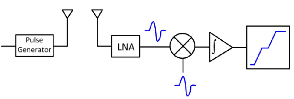
Fig. 1-1 Heterodyne transceiver………...…1
Fig. 1-2 UWB impulse radio transceiver architecture……….2
Fig. 2-1 Circuit diagram of pulse generator...6
Fig. 2-2 Illustration of pulse-formation process………..6
Fig. 2-3 Schematic of the new UWB, ultra-short-pulse transmitter. Bias circuits for the MESFET and amplifier are not shown...8
Fig. 2-4 Measured output pulse of the transmitter...10
Fig. 2-5 Pulse generator...11
Fig. 2-6 Simulation results...12
Fig. 2-7 Block diagram of the proposed G2(t) pulse generator...13
Fig. 2-8 CMOS G2(t) pulse generation circuit...13
Fig. 3-1 A new ultra-wideband monocycle pulse generator...16
Fig. 3-2 Input stage: (a) Active mode (b) Cutoff mode...17
Fig. 3-3 Under-damping (a), and critical-damping, over-damping response (b) of the second order transient response...18
Fig. 3-4 Simulation transient responses of V1 (a), VR (b) and VO (c)...20
Fig. 3-5 Photograph of monocycle pulse generator...22
Fig. 3-6 Measured output waveforms of the pulse generator at different control voltages Vcc...23
Fig. 4-1 Block diagram of the propose monocycle pulse generator...26
Fig. 4-2 Schematic of the proposed monocycle pulse generator...26
Fig. 4-3 The effect of the current starving cell...27
Fig. 4-4 The voltage waveform at node Vi_2 and Vi_3...28
Fig. 4-6 The ringing of the pulse is decreased by the over-damping response...31 Fig. 4-7 The amplitude of the monocycle pulse is adjustable and the voltage Vc
equals -2V(Vo1) and -2.42V(Vo2) respectively...32 Fig. 4-8 The duration of the monocycle pulse is 500 ps...32 Fig. 4-9 The chip photograph of the proposed pulse generator...44 Fig. 4-10 Measured output waveforms of the pulse generator at different control
voltages Vc...45 Fig. 4-11 Measured output waveforms with battery power supply of the pulse
generator at different control voltages Vc………47 Fig. 4-12 Shaping control circuit using the RC high filter………..50 Fig. 4-13 The comparison between RC filter (Black) and our work (Blue)………….51
Chapter 1
Introduction
1.1 Motivation
There are two dominant approaches for UWB wireless communications. The first one is based on the multi-band OFDM technique, which divides the spectrum into several sub-bands of 528 MHz each. The transceiver architecture here is very similar to that of a conventional wireless OFDM system. The second approach is based on an impulse radio (IR) technique which uses sub-nanosecond pulses to transmit data. The IR-technique offers the possibility of greatly simplifying the transceiver architecture. With the low emission limit in UWB, significant power savings can be achieved since the power amplifier (PA) can be omitted, which is truly advantageous for ultra low power applications. A UWB impulse radio can potentially use a bandwidth of over 7 GHz, reducing the chance of fading in a frequency selective channel, resulting in better immunity to destructive channel environments.
A comparison of a heterodyne transceiver and a UWB impulse radio transceiver architecture is shown in Fig. 1-1 and Fig. 1-2. It illustrates that the UWB impulse radio transceiver could be implemented as a simple integrated circuit chipset with very few off-chip components.
Fig. 1-2 UWB impulse radio transceiver architecture.
UWB transmitters transmit trains of extremely short pulses at precise time intervals, resulting in a very low power, noise-like signal that can coexist with other radio systems. Its features can be summarized as [1]:
z Ultra wideband and ultra-low PSD z Base-band communications
z Excellent immunity to interference from other radio systems z Excellent multipath immunity
z Low probability to intercept and detect
Ultra-wideband (UWB), ultra-short pulses are very attractive for radar and wireless communications applications. A UWB, ultra-short-pulse radar has spectrum extending from very low to very high frequencies [2] and, thus, can penetrate deeply lossy materials and achieve very fine resolution, such as ground penetrating radar (GPR) [3]. A UWB, ultra-short-pulse wireless communications system is also attractive for short-range applications, such as wireless personal area networks (WPANs), especially in a crowded spectrum environment, due to its low power spectral density that results in negligible interference with existing communications signals.
In general, there are three kinds of pulse waveform: Gaussian-like, monocycle, and polycycle pulses. The monocycle and polycycle pulses have band-pass frequency
spectrums, which result in less demanding design specifications for other system components (e.g., antennas). On the other hand, the monocycle waveform is commonly employed, as compared to the polycycle pulse, for its simpler realization and wider spectrum which is advantageous for high resolution and deep penetration [4].
1.2 Organization
In this thesis, we present two adjustable ultra-wideband (UWB) pulse generators using the second-order transient circuit to generate the adjustable monocycle pulse with good symmetry and low ringing. In Chapter 2, we discuss the structure and pulse generation methods of pulse generator.
In Chapter 3, we present a new ultra-wideband (UWB) monocycle pulse generator using two wideband bipolar junction transistors (BJTs) and a second-order transient circuit to generate a monocycle pulse. A voltage source can be applied to adjust the amplitude and duration of the pulse. This ultra-wideband pulse generator is fabricated with microstrip technology on FR4 printed circuit board.
In Chapter 4, we present an adjustable CMOS ultra- wideband (UWB) pulse generator using the second-order transient circuit as well to generate the adjustable monocycle pulse with good symmetry and low ringing. The rise time of the square wave can be adjusted to change the amplitude of the pulse for different requirements. This monocycle pulse generator is simulated and measured on TSMC 0.18μm CMOS technology. Finally, conclusions are made in Chapter 5.
Chapter 2
Introduction of UWB Pulse Generator
2.1 Introduction and Design of Pulse Generator
This chapter will introduce several pulse generators. They can be roughly sorted into two categories. The first is the pulse generated by step-recovery diode (SRD), and this kind of pulse generator is fabricated on PCB. Different from fabrication on PCB, the second kind is fabricated by CMOS integrated circuit technology.
The design of pulse generator has two targets. First, the pulse generator should be able to adjust the duration or amplitude of the pulse for different demands. Second, the pulse generator should have the characteristic of low power consumption. Generally there are four kinds of pulse generation methods listed as follows. First, several Gaussian-like impulses can be utilized to shape a 5th derivative of the Gaussian pulse [9]. Second, a second derivative Gaussian pulse can be generated by utilizing tanh(x) or other mathematic operations [10, 11]. Third, researchers utilize digital gates to compare two square waves with time difference to form a Gaussian impulse which further passes the filter to form the monocycle pulse [12-14]. Four, the pulse is generated from the step-recovery diode (SRD) and this pulse generator should be fabricated on PCB [5, 6].
2.2 Pulse Generator Using SRD
The ultra-wideband pulse generator which works in the sub-nanoseconds range is an important device for the ultra-wideband time-domain measurement systems. The pulse generator is used for both transmitter and receiver ends; for example, the UWB pulse generator converts data bits directly to ultra-short pulses at the transmitter, and the matched filter correlation receiver needs to use the pulse generator to generate a template pulse that matches the incoming pulse waveform. In the past, researchers employed the step-recovery diode (SRD) and pulse shaping circuit to generate the UWB pulse [4-7]. The SRD has a P-I-N structure, and the energy is stored in the intrinsic layer when the SRD is forward biased. On the other hand, when the SRD is under the reverse-bias, the stored energy will be discharged abruptly from the intrinsic layer. After discharging, the SRD abruptly stops conducting and then an impulse is generated [8].
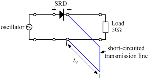
2.2.1 Uniplanar picosecond pulse generator using step-recovery diode [5]
This pulse generator employs SRD and delay line to generate an ultra-short pulse, and is fabricated completely on (uniplanar) coplanar waveguide (CPW). The use of delay line and uniplanar structure, in which all of the circuit elements are located on one side of the substrate, makes the circuit simple, compact, and low-cost. With an input square wave of 10 MHz repetition rate, the pulse generator produces pulses of 154ps pulsewidth and 3.5V amplitude with low ringing level and good symmetry.
Ω 50
d L
Fig. 2-1 Circuit diagram of pulse generator.
wave 2
wave 1
τ
Fig. 2-2 Illustration of pulse-formation process.
Fig. 2-1 is a circuit diagram of the pulse generator, which consists of an SRD and a short-circuited transmission line. A square-wave oscillator drives the SRD through a 50Ω transmission line and generates a step function. During a positive half-cycle of the signal of the oscillator, the SRD turned on (on state). The SRD still remains in that state within its lifetime even when the signal of the oscillator makes a transition to a negative half-cycle. It, however, turns off (off state) abruptly after its lifetime, under a negative half-cycle of the signal of the oscillator, to generate a step function the edge of which is proportional to the transition time of the SRD. When the state of the SRD is on, the energy of the oscillator is stored in the SRD. This energy is then discharged,
during the off state, into the transmission line as a step function. This step function divides into two step functions upon arriving at the junction between the main transmission line and the short-circuited transmission line; one step function propagates along the short-circuited transmission line and the other travels down the main transmission line towards the output port. The step function traveling towards the short circuit is reflected back, arrives at the output port after a certain time, and combines with the other step function to form a pulse at the output port. The short-circuited transmission line acts as a delay line effectively. The width of this pulse is approximately given as
p d u L 2 = τ (2.1) where up is the phase velocity along the short-circuited transmission line. We can
adjust the length Ld to change the pulsewidth τ.
Fig. 2-2 shows this pulse-forming process qualitatively where wave 1 is the step function propagating on the main transmission line and wave 2 is the step function reflected from the short-circuit termination.
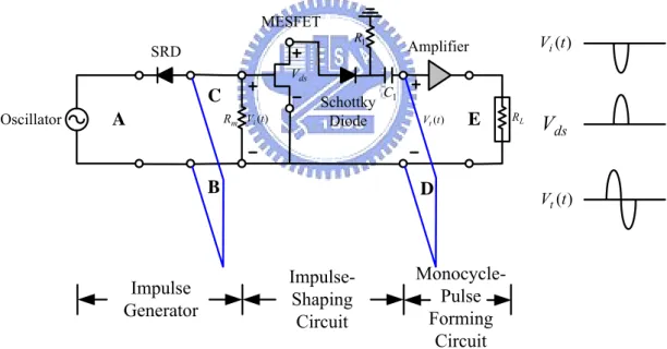
2.2.2 Novel low-cost ultra-wideband, ultra-short-pulse transmitter with MESFET impulse-shaping circuitry for reduced distortion and improved pulse repetition rate [6]
A new ultra-wideband, ultra-short-pulse transmitter has been developed using microstrip lines, step-recovery and Schottky diodes, a MESFET, and a monolithic microwave integrated circuit (MMIC) amplifier. A novel impulse-shaping network is implemented using MESFET to achieve several advantages. First, the MESFET impulse-shaping network converts the input voltage source into a current source,
which drives the SRD and hence allows the generation of the monocycle pulse’s half-cycle with little distortion. Second, it facilitates a broadband matching to the transmission line. This permits the use of high pulse repetition frequency (PRF) up to the limit of the employed SRD, which, in general, is several hundred MHz. Additionally, a wideband MMIC amplifier is used in the transmitter for amplification and isolation. The transmitter is realized on microstrip lines for low-cost manufacturation and produces monocycle pulses with 300-ps pulse width, about 2-V peak-to-peak amplitude, small ringing level, and good balance between the positive and negative half-cycles. It has been successfully used in short-range UWB radar for nondestructive subsurface sensing.
L R Amplifier A B C D E Schottky Diode MESFET SRD m R 1 C ) (t Vi Vt(t) 1 R Oscillator Impulse Generator Impulse-Shaping Circuit Monocycle-Pulse Forming Circuit ) (t Vi ds V ds V ) (t Vt
Fig. 2-3 Schematic of the new UWB, ultra-short-pulse transmitter. Bias circuits for the MESFET and amplifier are not shown.
Fig. 2-3 shows a circuit schematic of the new UWB monocycle-pulse transmitter, which consists of an impulse generator, an impulse-shaping network, a monocycle-pulse forming circuit, and a wideband amplifier.
The SRD, driven by an external local oscillator, generates a step function. This step function divides into two equal step functions propagating into the transmission lines
B and C. The step function traveling in the transmission line B is reflected back from
the short circuit, and eventually combines with the other step function in the transmission line C to form a negative impulse at the impulse generator’s output (i.e., at the gate of the MESFET). To prevent the gate-to-channel junction of the MESFET from entering the conduction region and maintain a reverse-biased junction without using an external negative bias voltage at the gate, the polarities of the SRD are arranged so that a negative step function is generated. It should also be noted that the combination of this negative voltage and the drain-source voltage should not exceed the avalanche breakdown level between the gate and drain of the MESFET.
The impulse-shaping circuitry is composed of a MESFET, a Schottky diode, a capacitor (C1), and resistors (R1 and Rm). The MESFET serves four functions. First, it
generates a positive impulse by inverting and amplifying the negative impulse arriving from the impulse generator. Second, it transfers a voltage source to a current source, which facilitates the formation of a less-distorted impulse. Third, it provides the isolation between the impulse generator and monocycle-pulse forming network. Fourth, it facilitates broadband matching to the transmission line due to a very large gate-source input impedance, thereby making it possible to increase the PRF. The resultant positive impulse turns on the Schottky diode and goes through a high-pass filter, formed by the capacitor C1 and the resistor representing the transient response
of the transmission line D. This filter allows only the leading and trailing parts of the impulse to transmit into the following monocycle-pulse forming network. The resistor
Rm at the gate of the MESFET serves as a wideband lossy matching circuit.
The monocycle-pulse forming circuit is realized using the short-circuited transmission line D and the transmission line E. It is used to convert an impulse into a
monocycle pulse. The impulse propagating toward the short circuit is reflected back and combines with the other impulse on the transmission line E to form a monocycle pulse at the input of the MMIC amplifier. The amplifier provides gain and also serves as an active isolator for the transmitter.
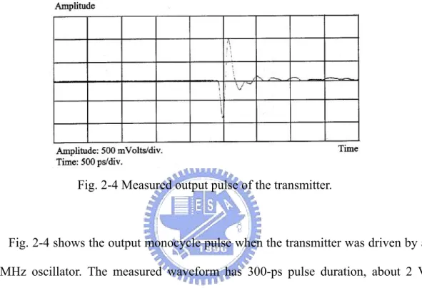
Fig. 2-4 Measured output pulse of the transmitter.
Fig. 2-4 shows the output monocycle pulse when the transmitter was driven by a 10-MHz oscillator. The measured waveform has 300-ps pulse duration, about 2 V (peak-to-peak).
2.3 CMOS Pulse Generator
2.3.1 All-digital low-power CMOS pulse generator for UWB system [9]
This pulse generator generates a single UWB pulse satisfying FCC regulations without any filtering.
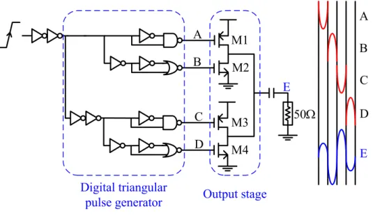
A B C D M1 M2 M3 M4 Digital triangular
pulse generator Output stage
E Ω 50 A B C D E
Fig. 2-5 Pulse generator.
Fig. 2-5 shows the proposed technique to generate the UWB pulse satisfying the FCC limitation. It consists of two blocks: a digital triangular pulse generator and an output stage to drive the 50Ω load. The digital triangular pulse generator provides the input signal to the subsequent stages. The input digital pulse and its inverted pulse which are followed by a NAND or NOR gate generate the triangular pulse. Since the NAND gate is low only when both inputs are high, and the NOR gate is high only when both inputs are low, the outputs of NAND and NOR gates are low and high at any given time, respectively. Each triangular pulse is designed to have the same peak-to-peak amplitude. To organize four phase signals correctly, as shown in Fig. 2-5, the delay time periods of the four pulses are determined by changing the size and number of the inverters. In the output stage, the four triangular pulses generated in the previous block are combined successively. The output current magnitude is controlled by the size of the output transistor (M1–M4). Power consumption is minimized by turning on only one MOS transistor in the output stage during each phase.
(a) (b) Fig. 2-6 Simulation results.
The whole circuit is designed using standard 0.18 μm CMOS technology with 1.8 V power supply and simulated in Cadence® environment with a Spectre® simulator. Fig. 2-6(a) shows the output voltage on 50 Ω load, and Fig. 2-6(b) shows the power spectral density (PSD) of an output voltage, obtained using SpectrumAnalyzer in ADS®. The output signal width is 380 ps, and -10 dB bandwidth is 7.2 GHz. The output voltage shape is similar to the 5th derivative of the Gaussian pulse, and the PSD of the output signal is located inside the spectrum given by the FCC regulation (shown in Fig. 2-6(b)). The maximum power consumption is 15.4 mW with 500 MHz pulse repetition frequency (PRF). The power consumption is reduced to 675 μW when the PRF is set to 1 MHz. The averaging power consumption is proportional to the PRF.
2.3.2 A novel CMOS UWB pulse generator [11]
A fully integrated CMOS pulse generation circuit is further proposed to generate the second derivative of Gaussian pulse G2(t). The block diagram of the proposed
pulse generator is shown in Fig. 2-7. It consists of three cascaded stages that implement square, exponential and second-order derivative functions, respectively.
2 2 dt x d
Fig. 2-7 Block diagram of the proposed G2(t) pulse generator.
Vdd=1.8V L C Vout(t) Ω = 50 L R M2 M1 R Vin(t) Vsqrt(t) i
Fig. 2-8 CMOS G2(t) pulse generation circuit.
The G2(t) pulse generation circuit implemented in CMOS process is shown in
Fig. 2-8. The square circuit is composed of transistor M1 and resistor R. When M1 is biased in saturation region, the drain voltage of M1 can be written as:
2 ) ( 2 in th in in sqr V V k R V R i V V = − × = − − . (2.2) If choosing th kV R= 2 , (2.3) the voltage Vsqr becomes
4 5 ) 2 3 ( 1 th 2 th in th sqr V V V V V =− − + , (2.4) where Vth < Vin < 2 Vth should be satisfied to keep M1 in the saturation region.
NMOS transistor M2 is biased in weak inversion region so that exponential I-V characteristics can be obtained as
λ λ κ κ / / 2 2 sqr GS V e V e DS e e I = = (2.5) Here κe and λ are process dependent parameters.
The second order derivation circuit is implemented by a RLC network in Fig. 2-8. The trans-impedance of the RLC network in s domain is
sC sL R L sR s I s V s T L L DS out 1 ) ( ) ( ) ( 2 + + = = . (2.6)
If taking the load resistance RL as 50 Ω, the approximation of RL + sL << 1/sC is
sufficiently accurate in the desired frequency rang (1-5 GHz). Thus the voltage Vout(t)
can be approximated as ) ( ) (s R LCs2I 2 s Vout ≈ L DS . (2.7) Obviously, the output voltage Vout(t) is a second derivative of the drain current
IDS2. By cascading the three stages as shown in Fig. 2-8, a G2(t) pulse generator is
Chapter 3
A New Ultra-Wideband Monocycle Pulse Generator Using
the Second-Order Transient Circuit
3.1 Introduction
In the past, researchers employed the step-recovery diode (SRD) and pulse shaping circuit to generate the UWB pulse [4-7]. The SRD has a P-I-N structure, and the energy is stored in the intrinsic layer when the SRD is forward biased. On the other hand, when the SRD is under the reverse-bias, the stored energy will be discharged abruptly from the intrinsic layer. After discharging, the SRD abruptly stops conducting and then an impulse is generated [8].
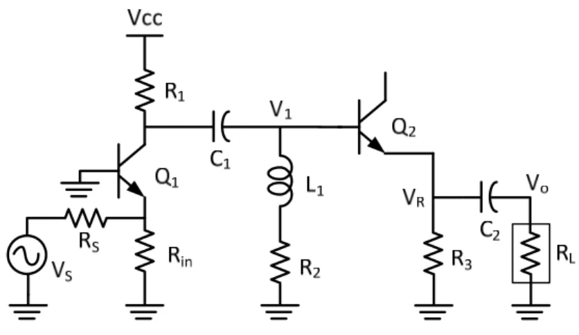
This chapter presents a new UWB monocycle pulse generator. Fig. 3-1 shows the schematic of the proposed new monocycle pulse generator. The pulse generator is composed of a BJT switch, a second-order transient circuit, a pulse-shaping network, and a differentiator. By Q1 and the second-order transient circuit (R1C1L1R2), an
impulse with a very short duration can be generated. The pulse ringing can be reduced by R2 and using a pulse shaping circuit composed of Q2,R3 and C2.Finally, the output
stage uses a simple RC differentiator to generate the monocycle pulse. This pulse generator can be fabricated with microstrip line technology. Our work shows that the pulse generator produces the monocycle pulse whose peak-to-peak amplitude ranges from 120 mV to 280 mV and duration ranges from 780 ps to 600 ps respectively.
Fig. 3-1 A new ultra-wideband monocycle pulse generator.
3.2 Circuit Operation and Analysis
3.2.1 Circuit description
Fig. 3-1 shows the schematic of the proposed new monocycle pulse generator. In the input stage, Q1 operates as an on/off switch between the active mode and the
cutoff mode. The middle stage is a second-order transient circuit which is composed of R1, C1, L1 and R2. Its function is to generate an impulse. The pulse shaping network
which is composed of Q2, R3 and C2 cuts off the low voltage ringing of the impulse
and increases the pulse amplitude tuning range.In the output stage, we utilize RL and
C2 to differentiate the impulse generated from the emitter of Q2 to produce a
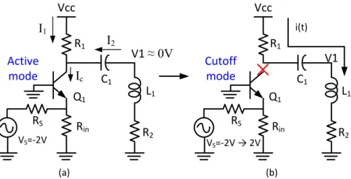
3.2.2 Input stage Vcc VS=‐2V Active mode I1 I2 Ic Vcc VS=‐2V → 2V Cutoff mode i(t) V1 ≈ 0V V1 (a) (b) Rin Q1 R1 C1 L1 R2 Rin Q1 R1 C1 L1 R2 RS RS
Fig. 3-2 Input stage: (a) Active mode (b) Cutoff mode.
The input stage, a common base (CB) network, functions as a switch which is shown in Fig. 3-2. The oscillator produces a ±2V square wave, VS, feeding into the
CB network.
When VS equals -2V, Q1 operates in the active mode as shown in Fig. 3-2(a).
Under such condition, Ic, I1, and I2 are DC currents and therefore V1 approximates to
zero volt because L1 looks like short circuit in DC current. At the same time, there is
no signal propagating to the base of Q2.
When VS changes from -2V to 2V, VBE1 is abruptly smaller than the threshold
voltage such that Q1 switches to the cutoff mode in a very short time. Therefore, the
collector current of Q1 is zero. Under such condition, the equivalent input impedance
seen into the collector of Q1 is infinity such that Q1 switches off. It results in the
R1C1L1R2 second-order transient circuit as shown in Fig. 3-2(b), and the impulse is
generated at node V1. Note that R2 should be selected a appropriate value in order to
obtain a symmetric monocycle pulse at the output of the pulse generator.
equations, dt t di L dt t i C R R t i Vcc ( )( ) 1 ( ) 1 ( ) 1 2 1+ + + =
∫
(3.1) 0 ) ( 1 ) ( ) ( 1 1 1 2 2 = = + + dt dVcc t i C L dt t di L R dt t i d (3.2) Equation (3.2) is a second order homogeneous ODE where coefficient R = R1+R2.Let the solution i(t)=kest, where k and s are constant coefficient, and we can derive s
as 0 1 ) ( 1 1 1 2 + + = C L s L R s (3.3) ∴ 2 2 2 1 2 1 1 1 1 1 1 2 1 1 ) , 2 ( 1 2 2 4 ) ( s s j L R C L j L R C L L R L R s =− ± − ≡− ± o − = − ± − = α ω α (3.4) where 1 1 1 C L o =
ω is the oscillation frequency and
1
2L
R
=
α is defined as the damping coefficient of the circuit.
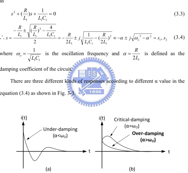
There are three different kinds of responses according to different α value in the equation (3.4) as shown in Fig. 3-3.
Fig. 3-3 Under-damping (a), and critical-damping, over-damping response (b) of the second order transient response.
When α >ωo, it is called the over-damping response which makes the energy stored in the inductor and the capacitor discharge from R in exponential decay manner.
The other cases are α =ωo and α <ωo . They are called the critical-damping response and the under-damping response respectively.
In order to reduce the ringing of V1, we let i(t) operate in over-damping mode. In
this work, we choose L1=3.3nH, C1=10pF, and R=125Ω so that α >ωo. Finally, the
solution i(t) in the over-damping case can be derived as
t C L L R L R t C L L R L R e k e k t i ) 1 ) 2 ( 2 ( 2 ) 1 ) 2 ( 2 ( 1 1 1 2 1 1 1 1 2 1 1 ) ( = − − − + − + − (3.4) Using equation (3.4) and the Kirchhoff’s law, we can obtain V1 as shown in
equation (3.5). The waveform of V1 is shown in Fig. 3-4(a) simulated from Agilent
ADS®. dt t di L R t i V1 = ( ) 2+ 1 ( ) (3.5) 118 119 120 121 122 123 117 124 0 1 2 -1 3 time, nsec V1, V (a)
118 119 120 121 122 123 117 124 -1 0 1 2 -2 3 time, nsec VR , V (b) 118 119 120 121 122 123 117 124 -400 -200 0 200 400 -600 600 time, nsec Vo, mV (c)
Fig. 3-4 Simulation transient responses of (a) V1, (b) VR and (c) VO.
3.2.3 Pulse shaping network and output stage
The pulse shaping network consists of a wideband BJT (Q2) used as a diode, a
resistance R3 and a capacitor C2. Fig. 3-4(b) is the Gaussian-like impulse resulting
pulse as shown in Fig. 3-4(c). When the pulse is at the rising edge, the diode (Q2)
turns on and the capacitor C2 is charged. On the other hand, when the pulse is at the
falling edge, the charged capacitor offers a reverse bias to the diode (Q2). This
operation makes the impulse VR similar to the Gaussian impulse and adds more tuning
range. Moreover, C2 and RL act as a differentiator to differentiate the Gaussian-like
impulse (VR) for generating a symmetric monocycle pulse. So the pulse shaping
network can keep symmetric waveforms and increase the pulse amplitude tuning range.
3.3 Fabrication and Measurement
We have fabricated the proposed monocycle pulse generator with microstrip line technology on a FR4 glass epoxy substrate of relative dielectric constant 4.4 and thickness 0.8 mm. Fig. 3-5 shows the photograph of the PCB pulse generator whose size is 46 mm * 23 mm. The product number of the BJT is BFG520 manufactured by Philip Semiconductor (NXP).
The measurement is made by using a 10-MHz square wave having 20-ns rise time and fall time respectively. Fig. 3-6 shows the measured monocycle pulse waveforms at different voltages Vcc. Vcc can vary the peak-to-peak amplitude of the monocycle pulse from 120 mV to 280 mV. The result also shows the pulse duration ranges from 600 ps to 780 ps with good symmetry between the positive and negative portion. The measurement result in Fig. 3-6 is similar with the simulation result in Fig. 3-4(c). Table 3-1 lists the component value of the proposed monocycle pulse generator.
Fig. 3-5 Photograph of monocycle pulse generator.
TABLE 3-1
COMPONENT VALUEOF THE PROPOSED MONOCYCLE PULSE GENERATOR
Component Value
R
in180
Ω
R
1100
Ω
C
110
pF
L
13.3
nH
R
225Ω
R
3620Ω
C
21
pF
478 480 482 484 486 476 488 -0.05 0.00 0.05 -0.10 0.10 time, nsec ''V o_ Vcc_ 4. 5V' '.. vo lta ge (a) Vcc = 4.5V 478 480 482 484 486 476 488 -0.10 -0.05 0.00 0.05 0.10 -0.15 0.15 time, nsec V o _V cc _5 V ..v o lta ge (b) Vcc = 5V
Fig. 3-6 Measured output waveforms of the pulse generator at different control voltages Vcc.
3.4 Comparison
Table 3-2 shows the comparison between our work and other proposed ones. From Table 3-2, we may observe that our pulse generator owns the characteristics of low ringing level and adjustability.
TABLE 3-2
COMPARISONOF THIS WORKTO OTHER PULSE GENERATORS
Ref. [6] [15] [16] [17] This work
Simulation/
Measurement Measurement Measurement
Peak-to-peak amplitude 1.75 V 700 mV 400 mV 300 mV~ 600 mV 120 mV~ 280 mV *Ringing level -17.3dB -20.9 dB -17 dB -16.9 dB~ -16 dB -20.5 dB~ -19.5 dB **Pulse duration 300 ps 350 ps 300 ps 200 ps~ 400 ps 600 ps~ 780 ps Technology SRD SRD SRD CMOS BJT
Adjustable No No No Yes Yes
Waveform Monocycle Monocycle
*Ringing level is defined as ⎥
⎦ ⎤ ⎢ ⎣ ⎡ − − − − pulse monocycle of value peak to peak The ringing of value peak to peak The log 20 .
**The pulse duration is defined as the time interval between the 10% points of the positive and negative peaks.
Chapter 4
An Adjustable CMOS Ultra-Wideband Pulse Generator
4.1 Introduction
Generally there are four kinds of pulse generation methods listed as follows. First, several Gaussian-like impulses can be utilized to shape a fifth derivative of the Gaussian pulse [9]. Second, a second derivative Gaussian pulse can be generated by utilizing tanh(x) or other mathematic operations [10, 11]. Third, researchers utilize digital gates to compare two square waves with time difference to form a Gaussian impulse which further passes the filter to form the monocycle pulse [12-14]. Four, the pulse is generated from the step-recovery diode (SRD) and this pulse generator should be fabricated on PCB [5, 6].
We present an adjustable CMOS ultra- wideband (UWB) pulse generator using the second-order transient circuit to generate the adjustable monocycle pulse with good symmetry and low ringing. The rise time of the square wave can be adjusted to change the amplitude of the pulse for different requirements. This pulse generator is simulated and measured on TSMC 0.18μm CMOS technology. Our simulation shows that the pulse generator produces the monocycle pulse whose peak-to-peak amplitude ranges from 50 mV to 220 mV and 500-ps pulse duration.
4.2 Circuit Operation and Analysis
This chapter presents a new CMOS UWB monocycle pulse generator. This pulse generator is composed of a square wave shaping circuit, a current starving cell, a pulse shaping control circuit, and a second order transient circuit as shown in Fig. 4-1. The circuit schematic was shown in Fig. 4-2. The square wave shaping circuit can decrease the rise time of the square wave and the current starving cell is used to adjust the rise time of the signal in order to have an adjustable amplitude of the monocycle pulse. In order to lower the effect of the process variation, the effective resistance of M13 is tuned for keeping a good symmetry of the pulse. The pulse shaping control circuit can change the symmetry of the monocycle pulse waveform. Finally, we use a current mirror to drive the second order transient circuit that can generate monocycle pulses.
Fig. 4-1 Block diagram of the propose monocycle pulse generator.
4.2.1 Square wave shaping circuit and current starving cell
The square wave shaping circuit is composed of two CMOS inverters. As shown in Fig. 4-3, the CMOS inverters are implemented to decrease the rise time of the square wave. So the square wave Vi_1 with fixed rise time is obtained. The fixed rise time of the square wave is beneficial for the input of the current starving cell.
The current starving cell can further control the rise time of the square wave in order to make pulse amplitude adjustable. We use the voltage Vc to control VGS of M9
and M10 which can change the current of M7 and M8. Therefore, the rise time can be varied to create different pulse amplitudes.
20 40 60 80 100 120 140 160 180 200 0 220 -1 0 1 -2 2 time, nsec Vi, V Vi_ 1 , V
4.2.2 Pulse shaping control circuit
The pulse shaping control circuit is composed of M11, M12, and M13. We treat M11 as a capacitor whose capacitance was about 30 fF in TSMC 0.18μm CMOS technology. When the voltage Vi_3 is negative where M12 and M14 is at off state, the output node Vo does not generate pulse. When Vi_2 is at the rising edge of the square waveform, M12 turns on and the voltage of Vi_3 in turn drives M14 on. The voltage of Vi_3 is increasing with Vi_2 and the monocycle pulse can be generated as shown in Fig. 4-4. Furthermore, because M13 can be regarded as a variable resistor, we can adjust Vgg to get a symmetric waveform of monocycle pulse for various process variation. 50 100 150 200 250 0 300 -1 0 1 -2 2 time, nsec Vi_ 2 , V Vi_ 3 , V
4.2.3 Second order transient circuit
We apply a pulse voltage to M14 for driving the current mirror M15 and M16. An impulse voltage is generated from the inductor L1. Generally the monocycle pulse have some ringing. We therefore use a resistor Rx to form the second order transient circuit operating in over-damping mode which can decrease the ringing of the pulse. Fig. 4-5 is the equivalent circuit diagram of the output stage of Fig. 4-2 where we let L1=L, C1=C, and R=Rx+RL. The transient response on the over-damping mode is deduced as follows.
Fig. 4-5 Diagram of the second order transient circuit.
Let the form of v(t) be e . We can apply the Kirchhoff’s law to the RLC loop st
and obtain the following equation as 0 ) 1 1 1 ( = + + sC R sL V (4.1)
Then, the characteristic equation of the transient circuit can be obtained as, 0 1 ) ( 2 + + = LC s L R s (4.2) Finally we can derive s from (4.2) as
2 1 2 2 2 , ) 2 ( 1 2 s s j L R LC j L R s o − = ± − ≡ − ± − = α ω α (4.3) where LC o 1 =
ω is the oscillation frequency and
L R
2 =
α is defined as the damping coefficient of the circuit.
When α > ωo,the value of s is negative and makes the energy stored in the
inductor and the capacitor discharges to R in the exponential decay manner. This condition is called the over-damping response of the second order transient circuit which can reduce the ringing of the monocycle pulse.
4.3 Simulation Results
The whole circuit simulations are completed in Agilent ADS®. We can observe the effect of the over-damping response in Fig. 4-6. There exists some ringing of the monocycle pulse as shown in Fig. 4-6(a) and the ringing of the monocycle pulse can be decreased by the over-damping response in Fig. 4-6(b). The voltage Vc can be adjusted to change the amplitude of the monocycle pulse whose peak-to-peak amplitude ranges from 50 mV to 220 mV in Fig. 4-7 and 500 ps of the pulse duration as shown in Fig. 4-8. We will discuss how process variation, temperature variation and voltage variation impact the symmetry of the monocycle pulse and how Vgg can adjust the symmetry of the monocycle pulse.
155 156 157 158 159 160 161 162 163 154 164 -100 -50 0 50 100 -150 150 time, nsec V o _NoRx , m V
(a) Rx=0Ω (Have ringing)
155 156 157 158 159 160 161 162 163 154 164 -50 0 50 -100 100 time, nsec Vo _W ith R x, mV (b) Rx=100Ω (Low ringing)
155 156 157 158 159 160 161 162 163 154 164 -100 -50 0 50 100 -150 150 time, nsec V o1, m V V o2, m V
Fig. 4-7 The amplitude of the monocycle pulse is adjustable and the voltage Vc equals -2V(Vo1) and -2.42V(Vo2) respectively.
158 160 162 156 164 -50 0 50 -100 100 time, nsec V o_500ps , m V
4.3.1 Process variation
Usually process variation will impact the performance of circuit. As shown in Table 4-1, process variation will change the symmetry of the monocycle pulse. Therefore, the voltage Vgg can adjust the symmetry of the monocycle pulse for the compensation of process variation.
Process variation: TT、FF、SS、FS、SF Simulation tool: Agilent ADS®
Simulation condition: TSMC 0.18μm CMOS technology Input square wave repetition rate: 10MHz
Output monocycle pulse duration: 500 ps Temperature: 25 ℃ TABLE 4-1 PROCESS VARIATION
Process variation
Simulation results
TT
T=25
℃158 160 162 156 164 -50 0 50 -100 100 time, nsec A ll_ P G _M on ocycl e_ F in al_ F or R ep or t_ T T ..V o, m V m8 m8 time= All_PG_Monocycle_Final_ForReport_TT..Vo=64.67mV159.5nsec
Vc=‐2.3V Vgg=0.503V
Symmetrical waveform
FF
T=25
℃158 160 162 156 164 0 5 10 -5 15 time, nsec A ll_ P G _M o no cycle _F in al _ F or R ep or t_ F F .. V o, m
Vc=‐2.3V Vgg=0.503V
Asymmetrical waveform
FF
T=25
℃158 160 162 156 164 -100 0 100 -200 200 time, nsec Al l_ PG _M onoc yc le_Fi nal _F or Repor t_ F F _Vgg0445V. .Vo m7 m7 time= All_PG_Monocycle_Final_ForReport_FF_Vgg0445V..Vo=137.5mV158.6nsec
Vc=‐2.3V Vgg=0.445V
Symmetrical waveform
SS
T=25
℃158 160 162 156 164 -40 -20 0 20 40 -60 60 time, nsec A ll_ P G _M on ocycle _ F in al_ F or R ep or t_ S S .. V o, m
Vc=‐2.3V Vgg=0.503V
Asymmetrical waveform
SS
T=25
℃158 160 162 156 164 -40 -20 0 20 40 -60 60 time, nsec Al l_ PG _M onoc yc le_Fi nal _F or Repor t_ SS_Vgg051V. .Vo, m m9 m9 time= All_PG_Monocycle_Final_ForReport_SS_Vgg051V..Vo=43.59mV160.1nsec
Vc=‐2.3V Vgg=0.51V
Symmetrical waveform
FS
T=25
℃158 160 162 156 164 -2 0 2 4 6 -4 8 time, nsec A ll_ P G _ M on o cycle _ F in al_ F o rR ep or t_ F S ..V o , m V
Vc=‐2.3V Vgg=0.503V
Asymmetrical waveform
FS
T=25
℃158 160 162 156 164 -100 -50 0 50 100 -150 150 time, nsec All_ PG _Mo n oc ycle _ Fin a l_Fo rRep ort _FS_V gg 044 5V ..V o , m V m11 m11 time= All_PG_Monocycle_Final_ForReport_FS_Vgg0445V..Vo=110.6mV159.7nsec
Vc=‐2.3V Vgg=0.445V
Symmetrical waveform
SF
T=25
℃156 158 160 162 164 166 154 168 -50 0 50 -100 100 time, nsec A ll_ P G _M on ocycl e_ F in al_ F or R ep or t_ S F ..V o, m V m12 m12 time= All_PG_Monocycle_Final_ForReport_SF..Vo=62.06mV159.0nsec
Vc=‐2.3V Vgg=0.503V
Symmetrical waveform
Input signal (Function generator HP‐3325B)20 40 60 80 100 120 140 160 180 200 0 220 -1 0 1 -2 2 time, nsec Vi, V
4.3.2 Temperature variation
As shown in Table 4-2, temperature variation will also change the symmetry of the monocycle pulse.
Temperature variation: 0℃、25℃、85℃ Corner case=TT
TABLE 4-2 TEMPERATURE VARIATION
Temperature
variation
Simulation results
T=0
℃158 160 162 156 164 -100 -50 0 50 -150 100 time, nsec A ll_ P G _M on ocycl e_ F in al_ F or R ep or t_ 0C ..V o, m m13 m13 time= All_PG_Monocycle_Final_ForReport_0C..Vo=84.76mV159.5nsec
Vc=‐2.3V Vgg=0.503V
Asymmetrical waveform
T=0
℃158 160 162 156 164 -100 -50 0 50 100 -150 150 time, nsec A ll_ P G _ M onoc yc le_F inal _For R epor t_0 C _Vgg0483V. .V m15 m15 time= All_PG_Monocycle_Final_ForReport_0C_Vgg0483V..Vo=96.93mV159.4nsec
Vc=‐2.3V Vgg=0.483V
Symmetrical waveform
T=25
℃158 160 162 156 164 -50 0 50 -100 100 time, nsec Al l_ P G _M on ocycl e_ F in al_ F or R ep or t_ 25 C ..V o, m m14 m14 time= All_PG_Monocycle_Final_ForReport_25C..Vo=64.70mV159.5nsec
Vc=‐2.3V Vgg=0.503V
Symmetrical waveform(Typical)
T=85
℃156 157 158 159 160 161 162 163 164 165 155 166 -0.5 0.0 0.5 -1.0 1.0 time, nsec A ll_ P G _ M o no cycl e _F in a l_ F or R e po rt _8 5 C .. V o , m
Vc=‐2.3V Vgg=0.503V
Asymmetrical waveform
T=85
℃156 158 160 162 154 164 -40 -20 -0 20 40 60 -60 80 time, nsec Al l_ P G _ M on oc yc le_ F ina l_ F o rR ep or t_ 8 5C _ Vg g 04 5V ..V o, m m16 m16 time= All_PG_Monocycle_Final_ForReport_85C_Vgg045V..Vo=62.84mV159.3nsec
Vc=‐2.3V Vgg=0.45V
Asymmetrical waveform
4.3.3 Voltage variationAs shown in Table 4-3, voltage variation will also change the symmetry of the monocycle pulse and the voltage Vgg can also adjust the symmetry of the monocycle pulse.
Voltage variation: Vcc(1.8V) and Vss(-1.8V) ±10% Corner case=TT
TABLE 4-3 VOLTAGE VARIATION
Voltage variation
Simulation results
Vdd = 1.8V
Vss = ‐1.8V
158 160 162 156 164 -50 0 50 -100 100 time, nsec A ll_P G _M onoc yc le_F inal _For R epor t_V dd_1 V 8. .V o, m V m17 m17 time= All_PG_Monocycle_Final_ForReport_Vdd_1V8..Vo=63.28mV159.5nsecVc=‐2.3V Vgg=0.503V
Symmetrical waveform(Typical)
Vdd = 1.98V
Vss = ‐1.98V
158.2 160.2 162.2 156.2 164.0 -100 0 100 -200 200 time, nsec A ll_P G _M onocy cl e _F inal _For R epo rt _V dd_1V 98. .V o, m V m18 m18 time= All_PG_Monocycle_Final_ForReport_Vdd_1V98..Vo=148.8mV158.1nsecVc=‐2.3V Vgg=0.503V
Symmetrical waveform
Vdd = 1.62V
Vss = ‐1.62V
156 158 160 162 164 166 168 170 154 172 -50 0 50 100 150 -100 200 time, nsec A ll_ P G _M on ocycle _F in a l_ F or R e po rt _V dd _1 V 62 ..V o, u VVc=‐2.3V Vgg=0.503V
Asymmetrical waveform
Vdd = 1.62V
Vss = ‐1.62V
156 158 160 162 164 166 168 170 172 154 174 -5 0 5 -10 10 time, nsec A ll_ P G _M on ocycl e_ F in al _F or R ep or t_ V dd _1 V 62_V gg045V .. V o, m V m19 m19 time= All_PG_Monocycle_Final_ForReport_Vdd_1V62_Vgg045V..Vo=8.435mV161.9nsecVc=‐2.3V Vgg=0.45V
Symmetrical waveform
4.4 Fabrication and Measurement
This pulse generator is measured and fabricated on TSMC 0.18μm CMOS technology. Fig.4-9 shows the microphotograph of the proposed pulse generator whose size is 0.868mm * 0.457mm.
The measurement is made by using a 10-MHz square wave having 20-ns rise time and fall time respectively. Fig.4-10 shows the measured Gaussian pulse waveforms at different Vc. Change of Vc can result in the peak amplitude of the Gaussian pulse from 18 mV to 30 mV. The result also shows the 300-ps pulse duration with low ringing which results from the over-damping effect of the second order transient circuit.
If smaller value of capacitor C1 is chosen in simulation, the monocycle pulse will be asymmetric. Therefore, we instead use a large capacitor C1 to get a monocycle pulse with low ringing. However, from the measurement result, the monocycle pulse can not be generated for the large capacitor C1. A possible solution to modify this work is to connect a broad band amplifier which can amplify the Gaussian pulse and a high pass filter to differentiate the Gaussian pulse.
Fig. 4-9 The microphotograph of the proposed pulse generator. 40 42 44 46 38 48 -0.02 -0.01 0.00 0.01 -0.03 0.02 time, nsec V c_n2V 2. .v olt age (a)
40 42 44 46 38 48 -0.02 -0.01 0.00 0.01 -0.03 0.02 time, nsec vo lta ge (b)
Fig. 4-10 Measured output waveforms of the pulse generator at different control voltages Vc.
4.4.1 Measurement with battery power supply
We use batteries and regulated power supply ICs, LM317 and LM337, to obtain pure DC sources. From this measurement, the amplitude of the tuning range of Gaussian pulse is increased. The following figures show the amplitude of Gaussian pulse for different control voltage, Vc. Table 4-4 lists the simulation and measurement results of the proposed pulse generator.
38 40 42 44 46 36 48 -0.005 0.000 0.005 0.010 0.015 -0.010 0.020 time, nsec ''V c_n1. 3V _V gg_ 0. 3V ''. .v ol ta ge (a) Vc = -1.3V 38 40 42 44 46 36 48 -0.005 0.000 0.005 0.010 0.015 -0.010 0.020 time, nsec ''V c_ n1 .5V _V gg_ 0. 3V ''. .v olt age (b) Vc = -1.5V 38 40 42 44 46 36 48 -0.005 0.000 0.005 0.010 0.015 -0.010 0.020 time, nsec ''V c_n 1. 8V _V gg _0. 3V ''. .v ol tage (c) Vc = -1.8V
38 40 42 44 46 36 48 -0.005 0.000 0.005 0.010 0.015 -0.010 0.020 time, nsec ''V c_n 2V _V gg_0 .3V ''. .v ol tag e (d) Vc = -2V 38 40 42 44 46 36 48 -0.005 0.000 0.005 0.010 0.015 -0.010 0.020 time, nsec ''V c_n2. 2V _V gg_0 .3 V ''. .v olt ag e (e) Vc = -2.2V
Fig. 4-11 Measured output waveforms with battery power supply of the pulse generator at different control voltages Vc.
TABLE 4-4
PERFORMANCEOF THE MONOCYCLE PULSE GENERATOR Simulation Measurement (Power Supply) Measurement (Battery) Process Technology TSMC 0.18μm CMOS Pulse
Waveform Monocycle pulse Gaussian pulse Gaussian pulse Pulse Width 450 ps 300 ps 270ps ~ 470 ps (Vp-p) 53 mV ~ 214 mV 18 mV ~ 30mV 6 mV ~ 20mV Chip Area 0.397 mm 2 (0.868mm * 0.457mm)
4.5 Comparison
Table 4-5 shows the comparison of this work to other pulse generators. From Table 4-5, we present a pulse generator of low ringing level and adjustability.
TABLE 4-5
COMPARISONOF THIS WORK TO OTHER PULSE GENERATORS
Ref. [12] [18] [19] This work
Simulation/
Measurement Simulation Simulation
Peak-to-peak
amplitude 22.97 mV 200 mV 110 mV
53 mV~ 214 mV Ringing level -24.9 dB N/A -17.8 dB -40.5 dB~
-26.6 dB Pulse
duration 450 ps 250 ps 170 ps 450 ps
Technology CMOS Bi-CMOS CMOS CMOS
Adjustable No Yes
Waveform Monocycle Monocycle
4.6 Discussion
4.6.1 Pulse shaping control circuit using RC high pass filter
We will discuss the pulse shaping control circuit which uses the RC high pass filter as shown in Fig. 4-12. The comparison between RC high pass filter and our work is shown in Fig. 4-13. The black color line is the response of RC high pass filter and the blue color line is that of our proposed circuit. We use a RC high pass filter as a pulse shaping control circuit. It can not quickly turn off M14, so the output waveform Vo is not a monocycle pulse but a Gaussian pulse. The simulation of our work shows
that the fall time of Vi_3 is too short in Fig. 4-13(a). Practically this waveform can not be realized. Similarly, since the voltage waveform Vi_3 of our work also has a very short fall time duration, our work is not able to turn off M14 quickly either. As a result, the voltage waveform VL is not a Gaussian pulse, and the resultant voltage waveform Vo is a Gaussian pulse rather than a monocycle pulse. Finally we propose several methods to modify this work.
Vdd Vdd Vdd Vss Vc Vi M1 M2 M3 M4 Rx M5 M6 M10 M9 M7 M8 M14 M15 M16 Vss Vdd Vdd Vdd Vss Vss R1 R2 L1 C1 R3
Vi_1 Vi_2 Vi_3
VL Vo
RL CA
RA
Fig. 4-12 Shaping control circuit using the RC high filter.
154 156 158 160 162 164 166 168 170 172 152 174 0.0 0.5 1.0 1.5 -0.5 2.0 time, nsec Vi _3 , V _9 60 829 _t es t. .V i_3, V (a)
158 160 162 164 166 156 168 0 200 400 600 -200 800 time, nsec VL , mV _9 60 82 9_ te st .. V L, m V (b) 156 158 160 162 164 154 166 -50 0 50 100 150 -100 200 time, nsec Vo , mV _9 60 82 9_ te st .. V o, m V (c)
Fig. 4-13 The comparison between RC filter (Black) and our work (Blue).
4.6.2 Methods to modify this pulse generator
Because the output waveform Vo on measurement is not a monocycle pulse but a Gaussian pulse, we propose some possible methods to modify this work. The first is to design a pulse shaping control circuit which can generate a short pulse to quickly turn on and turn off M14. For example, we can utilize a NAND gate whose input signals are two square waves with time difference to generate a short pulse for driving
M14. Moreover, since the output waveform Vo is a Gaussian pulse in the measurement, another method is to connect a wideband amplifier in our work which can increase isolation and connect a high pass filter to differentiate the Gaussian pulse and generate the monocycle pulse.
Chapter 5
Conclusion
Two new UWB monocycle pulse generators have been designed, fabricated and measured in this thesis. First, we fabricate a monocycle pulse generator using two BJTs and a second-order transient circuit. The monocycle pulse duration ranges from 600 ps to 780 ps with good symmetry and low ringing. Vcc can vary the peak-to-peak amplitude of the monocycle pulse from 120 mV to 280 mV. Second, we use TSMC CMOS process to fabricate a pulse generator. The inductor L1 is used to generate the impulse and differentiate it to get the monocycle pulse. The ringing of the pulse can be decreased by using the over-damping technique of the second order transient circuit. From the measurement results, Vc can vary the peak amplitude of the Gaussian pulse from 18 mV to 30 mV. The result also shows the 300 ps pulse duration with low ringing.The voltage-adjustable characteristic makes both the proposed pulse generators applicable in many UWB systems.
References
[1] P. Withington, Impulse Radio Overview, Time Domain Corp.
[2] IEEE 802.15 WPAN High Rate Alternative PHY Task Group 3a (TG3a). Available: http://www.ieee802.org/15/pub/TG3a.html.
[3] R. J. Fontana, "Recent Applications of Ultra Wideband Radar and Communications Systems", EuroEM 2000, Edinburgh, Scotland, 30 May 2000, published in Ultra-Wideband, Short-Pulse Electromagnetics, Kluwer Academic/Plenum Publishers, 2000.
[4] X. Chen and S. Kiaei, “Monocycle shapes for ultra wideband system”, IEEE
international symposium on circuits and systems (ISCAS 2002), vol. 1, pp.
597-600, May 2002.
[5] J. S. Lee and C. Nguyen, “Uniplanar picosecond pulse generator using step-recovery diode”, Electronics Letters, vol. 37, no. 8, pp. 504-506, Apr. 2001. [6] J. S. Lee and C. Nguyen, “Novel low-cost ultra-wideband, ultra-short-pulse
transmitter with MESFET impulse-shaping circuitry for reduced distortion and improved pulse repetition rate”, IEEE Microwave Wireless Components Letters, vol. 11, no. 5, pp. 208-210, May 2001.
[7] J. Han and C. Nguyen, “A new Ultra-Wideband, Ultra-short Monocycle Pulse Generator With Reduced Ringing”, IEEE Microwave Wireless Components
Letters, vol. 12, no. 6, pp. 206-208, Jun. 2002.
[8] J. S. Lee, C. Nguyen and T. Scullion, “New Uniplanar Subnanosecond Monocycle Pulse Generator and Transformer for Time-Domain Microwave”,
IEEE Transactions on Microwave Theory and Techniques, vol. 49, no. 6, pp.
1126-1129, Jun. 2001.
[9] H. Kim, D. Park, and Y. Joo, “Alldigital lowpower CMOS pulse generator for UWB system”, Electronics Letters, vol. 40, no. 24, pp. 1534-1535, Nov. 2004.
[10] J. F. M. Gerrits and J.R. Farserotu, “Wavelet generation circuit for UWB impulse radio applications”, Electronics Letters, vol. 38, no. 25, pp. 1737-1738, Dec. 2002.
[11] Y. Zheng, H. Dong and Y. P. Xu, “A novel CMOS/BiCMOS UWB pulse generator and modulator”, 2004 IEEE MTT-S International Microwave
Symposium Digest, vol. 2, pp. 1269-1272, Jun. 2004.
[12] Y. Jeong, S. Jung and J. Liu, “A CMOS impulse generator for UWB wireless communication systems”, in Proceedings of International Symposium on Circuits
and Systems (ISCAS 2004), vol. 4, pp. 129-132, May 2004.
[13] X. Zhang, S. Ghosh and M. Bayoumi, “A low power CMOS UWB pulse generator”, Symposium on Circuits and Systems, vol. 2, pp. 1410-1413, Aug. 2005.
[14] B. Jung, Y. H. Tseng, J. Harvey and R. Harjani, “Pulse generator design for UWB IR communication systems”, IEEE International Symposium on Circuits and
Systems (ISCAS 2005), vol. 5, pp. 4381–4384, May 2005.
[15] J. S. Lee, C. Nguyen and T. Scullion, “New uniplanar subnanosecond monocycle pulse generator and transformer for time-domain microwave applications”, IEEE
Transactions on Microwave Theory and Techniques, vol. 49, no. 6, part 1, pp.
1126-1129, Jun. 2001.
[16] J. Han and C. Nguyen, “A new ultra-wideband, ultra-short monocycle pulse generator with reduced ringing”, IEEE Microwave and Wireless Components
Letters [see also IEEE Microwave and Guided Wave Letters], vol. 12, no. 6, pp.
206-208, Jun. 2002.
[17] M. Miao and C. Nguyen, “On the Development of an Integrated CMOS-Based UWB Tunable-Pulse Transmit Module”, IEEE Transactions on Microwave
Theory and Techniques, vol. 54, no. 10, pp. 3681–3687, Oct. 2006.
[18] S. Bagga, W. A. Serdijn and J. R. Long, “A PPM Gaussian monocycle transmitter for ultra-wideband communications”, in Proceedings International
[19] T. K. K. Tsang and M. L. El-Cramal, “Fully integrated sub-microWatt CMOS ultra wideband pulse-based transmitter for wireless sensors networks”, IEEE
International Symposium on Circuits and Systems (ISCAS 2006), pp. 4, May