A Low-Phase-Noise Area-Efficient 3-D LC VCO in
Standard 0.18-um CMOS Technology
Hsiao-Chin Chen, Tao Wang and Shey-Shi Lu
Graduate Institute of Electronics Engineering National Taiwan University
Taipei, Taiwan
Guo-Wei Huang
Nano Device Laboratory Hsin-chu, Taiwan
Abstract—A miniaturized (0.224 mm2
) 4.5~5.0 GHz 3-D LC VCO possessing area-efficient metal-6 on-chip inductors is implemented in 0.18 um 1P6M CMOS technology. With inductors directly above the other devices, this VCO shows a measured phase noise of -124.6 dBc / Hz at 1 MHz offset from the 4.9 GHz carrier while dissipating 24 mW. The figure-of-merit (-184.7 dBc/Hz) achieved is better than most of the previous state-of-art results of the CMOS LC VCOs while occupying only half the die area.
I. INTRODUCTION
Inductors are important passive devices for the building blocks of radio-frequency (RF) circuits such as voltage controlled oscillators (VCOs), low noise amplifiers (LNAs), and power amplifiers (PAs). Monolithic inductors are definitely the best solution to the single chip wireless communication systems. Thanks to the advance of semiconductor technology, monolithic inductors with moderate quality factor Q (8~10) at GHz-band are now available in CMOS technologies and widely used in commercial radio-on-a-chip products [1] [2]. However, these monolithic spiral inductors occupy considerable precious die area (~ 0.3 mm x 0.3 mm) and hence handicap a high-density integration. Compact circuit designs which occupy small die area are always desirable, as area-efficient designs directly translate into reduction in cost [3]. In order to minimize the die area of the RF building blocks and enhance the Q values of inductors simultaneously, the concept of fabricating inductors with a thick dielectric layer (usually polyimide) above ICs by post-IC processing technology has also been proposed and realized [4] – [7]. However, excess cost and production complexity prevent the post-processing technology from wide-spread applications. It has been demonstrated by [8] – [10] that excellent phase noise performance can still be achieved even for those VCOs with low Q (< 10) inductors if the VCOs are optimally designed. Consequently, it may not be necessary to fabricate high-Q inductors above the IC by post-processing. Alternatively, a simpler solution to reducing the die size is to place the circuits under the low-Q inductors fabricated by standard CMOS metal interconnect
technology and thus reuse the occupied area of the on-chip inductors. To some extent, on-chip inductors must electromagnetically interact with the devices in their neighborhood. However, we are not aware of any report on how severely the circuit performance is affected by such interaction. On the contrary, it has been proven recently that such interaction makes no apparent impact on the operation of N-MOSFETs [11].
In this paper, a three-dimensional LC VCO with active and passive devices placed under the metal-6 on-chip inductors is implemented in a standard 0.18 um 1P6M CMOS technology. To our knowledge, this area-efficient topology has never been realized on RF circuits operating at GHz-band and hence the results of this work are important to the RF design community.
II. CIRCUIT DESIGN
The frequency range (4824 MHz ~ 4960 MHz) of the VCO is targeted to be twice the application band of the most popular WLAN, i.e. 802.11b/g, so that the LO pulling effect can be alleviated in a direct conversion transceiver using this VCO followed by a divide-by-2 circuit. The schematic of our 3-D LC VCO is shown in Fig.1.
Fig.1 VCO schematic
IEEE MELECON 2006, May 16-19, Benalmádena (Málaga), Spain
The cross-coupled PMOS pair is used to generate the negative conductance required for the sustaining of a stable oscillation. Instead of an FET current source, a polysilicon resistor which is substantially free of 1/f noise is used to define the tail current [12] [13].
The oscillation frequency is determined by the accumulation-mode N-MOSFET varactors and the in-house designed inductors, which are made of the metal-6 (M6) of the 1P6M CMOS technology and placed closely (< 5 um) above the cross-coupled pair to save the precious die area as shown in Fig.2. The total die area excluding the testing pad of control voltage is 0.224 mm2, which is almost half the die area of the VCO with a traditional layout [14] where the inductor is placed alongside the other devices instead of above them.
Fig.2 A perspective view of the 3-D LC VCO. The PMOS cross-coupled pair, biasing resistors, and capacitors are placed under the in-house designed inductors made of the top-metal layer (M6) of 1P6M CMOS technology and hence almost 50 % reduction in VCO die size compared to traditional design is achieved.
The desired inductance is estimated to be about 0.6~0.7nH. The geometrical feature of the in-house designed inductor is shown in the Fig.3 (a). After several iterations, an inner area of 787 um x 285 um is determined.
(a)
(b)
Fig.3 In-house designed area efficient inductors: (a) layout; (b) model parameters obtained by the EM simulation of ADS Momentum
The EM simulation provided by ADS Momentum is applied to the inductor layout and the extracted model parameters are shown in the Fig.3 (b). Note that because of this carefully designed in-house inductor, the die area of VCO is efficiently minimized. Fig.4 shows the microphotograph of the fabricated 3-D LC VCO.
Fig.4 The microphotograph of the 3-D LC VCO. The total die area excluding the testing pad of control voltage is only 0.224 mm2.
III. RESULTS AND DISCUSSION
The core of the VCO draws a current of 10 mA from a 2.4 V supply. The characteristics of the VCO are measured by Agilent Signal Source Analyzer (HP E5052A) in a shielding chamber. Fig.5 shows the measured tuning range of the VCO. Clearly, the VCO carrier frequency can be varied from 4519 MHz to 5019 MHz, covering the required specification of 4824 MHz ~ 4960 MHz.
Fig.5 Measured VCO tuning range. The 3-D VCO operates from 4519 to 5019 MHz, corresponding to a center frequency of 4769 MHz and tuning range of 10.5 %.
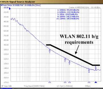
The measured phase noise is shown in Fig.6. Phase noises of -118.5 dBc / Hz and -124.6 dBc / Hz are obtained at 600 kHz and 1 MHz offsets, respectively, from the carrier frequency of 4945.7 MHz. The achieved phase noise performance meets the WLAN 802.11b/g requirements marked in Fig.6.
Fig.6 Measured VCO phase noise. Phase noises of 118.5 and -124.6 dBc / Hz are obtained at 600 kHz and 1 MHz offsets, respectively, from the carrier frequency of 4945.7 MHz.
For a fair comparison of VCOs with different oscillation frequencies and power consumption, the widely-accepted power-frequency-normalized figure-of-merit (FOM) [15] given below is calculated for recently reported 4~6 GHz VCOs [14] - [19] and summarized in Table I.
{ }
( )1 0 2 sup log 10 L f f f P PFN off off + ⎟⎟⎠ ⎞ ⎜⎜⎝ ⎛ ⎥ ⎥ ⎥ ⎥ ⎦ ⎤ ⎢ ⎢ ⎢ ⎢ ⎣ ⎡ • =, where L{foff} represents the SSB phase noise measured at
the offset frequency foff from the carrier frequency f0 and Psup
is the power consumption in mW.
TABLE I SUMMARY of 4~ 5 GHz MONOLITHIC LC VCOs (phase noise and FOM at 1MHz offset)
PDC (mW) FOSC (GHz) Phase noise (dBc/Hz) Tuning Range (%) FOM (dBc/Hz) Chip area (mm2) This work 24 4.9 -124.6 10.5 -184.7 0.224 [14] 5.9 5.6 -116.7 11.3 -184.0 0.392 [15] 17.3 5.3 -126.0 3.8 -188.2 0.705 [16] 7.5 4.0 -117.0 13.0 -180.3 0.500 [17] 7 5.0 -117.0 21.3 -182.4 N.A. [18] 7 5.6 -116.0 5.6 -182.5 N.A. [19] 5 5.8 -112.0 12.8 -180.3 N.A.
From Table I, it is clear that the FOM of this 3-D VCO is better than most of published results while occupying the
smallest die area. The best FOM is achieved by the VCO in [15], where the good phase noise performance may be partly resulted from connecting a pair of high Q MIM capacitors in parallel with the tank of the VCO. However, this improvement in phase noise is achieved at the expense of reduction in tuning range because the variable capacitance in percentage is decreased by this way.
IV. CONCLUSION
A 4.5~5.0 GHz area-efficient 3-D LC VCO with active transistors and passive capacitors/resistors placed under the inductors made of top-metal by standard CMOS interconnect technology is designed and implemented. Consequently, the die size of this 3-D VCO is solely determined by the area of the inductor and almost 50 % reduction in die size can be achieved. Experimental results show that a phase noise of -124.6 dBc / Hz at 1 MHz offset from the 4.9 GHz carrier with power consumption of 24 mW is obtained. The achieved phase noise performance meets the 802.11b/g requirements and the calculated FOM is better than most of the previous state-of-the-art results while demanding smaller die area. It is believed the RF industry can benefit from this area-efficient topology in the future.
ACKNOWLEDGMENT
Financial supports from national science council under no. 942215E002032/942218E002045 and chip fabrication from UMC are appreciated.
REFERENCES
[1] M. Zagari, D. K. Su, C. P. Yue, S. Rabii, D. Weber, B. J. Kaczynski, S. S. Mehta, K. Singh, S. Mendis, B. A. Wooley, “5-GHz CMOS transceiver for IEEE 802.11a wireless LAN system,” IEEE J. Solid-State
Circuits, vol. 37, pp. 1688-1694, December 2002.
[2] A. Behzad, L. Lin, Z. M. Shi, S. Anand, K. Carter, M. Kappes, E. Lin, T. Nguyen, D. Yuan, S. Wu, Y. C. Wong, V. Fong, A. Rofougaran, “Direct-conversion CMOS transceiver with automatic frequency control for 802.11a wireless LANs,” ISSCC Dig. Tech.
Papers, vol. 1, pp. 356-499, 2003.
[3] T. K. K. Tsang and M. N. El-Gama1, “A high figure of merit and area-efficient low-voltage (0.7-1 V) 12 GHz CMOS VCO,” RFIC Symposium, pp. 89-92, 2003.
[4] M.-S. Lin, “Inductor structure for high performance system-on-chip using post passivation process,” US paternt 6455885, September 2002.
[5] J.-M. Karam, F. Valentin, A. Mhani, L. Basteres, “Monolithic integrated circuit incorporating an inductive component and process for fabricating
WLAN 802.11 b/g
requirements
such an integrated circuit,” US patent 6459135, October 2002.
[6] E.-C. Park, Y.-S. Choi, J.-B. Yoon, S. Hong, and E. Yoon, “Fully integrated low phase noise VCOs with on-chip MEMS inductors,” IEEE MTTs, pp. 289-296, vol. 51, no. 1, January 2003.
[7] B. Piernas, K. Nishikawa, K. Kamogawa, and I. Toyoda, “Three-dimensional MMIC technology on silicon: review and recent advances,” IEICE
TRANSACTIONS on ELECTRON, pp. 1394-1403,
vol. E85-C, no. 7, July 2002.
[8] D. Ham, and A. Hajimiri, “Concept and methods in optimization of integrated LC VCOs,” IEEE J.
Solid-State Circuits, pp. 896-909, vol. 36, no. 6, June 2001.
[9] R. Aparicio, and A. Hajimiri, “A noise-shifting differential Colpitts VCO,” IEEE J. Solid-State
Circuits, pp. 1728-1736, vol. 37, no. 12, December
2002.
[10] J. Lin, “An integrated low-phase-noise voltage controlled oscillator for base station applications,”
ISSCC Dig. Tech. Papers, pp. 432-433, 2000..
[11] Y. Papananos, and N. Nastos, “Inductor over MOSFET: operation and theoretical study of a CMOS RF three-dimensional structure,” PROC. 24th
INTERNATIONAL CONFERENCE on MICROELECTRONICS, pp. 525-529, vol. 2, May
2004.
[12] E. Hegazi, H. Sjoeland, and A. A. Abidi, “A filtering technique to lower LC oscillator phase noise,” IEEE
J. Solid-State Circuits, pp. 1921-1930, vol. 36, no. 12,
December 2001.
[13] T. Maeda, H. Yano, T. Yamase, N. Yoshida, N. Matsuno, S. Hori, K. Numata, R. Walkington, T.
Tokairin, Y. Takahashi, M. Fujiii, and H. Hida, “A direct-conversion CMOS transceiver for 4.9-5.95GHz multi-standard WLANs,” ISSCC Dig. Tech.
Papers, 2004.
[14] T. Song, S. Ko, D.-H. Cho, H.-S. Oh, C. Chung, and E. Yoon, “A 5GHz transformer-coupled CMOS VCO using bias-level shifting technique,” RFIC
Symposium, pp. 127-130, 2004.
[15] T. Y. Kim, A. Adams, and N. Weste, “High performance SOI and bulk CMOS 5GHz VCOs,”
RFIC Symposium, pp. 93-96, 2002.
[16] J. Maget, M. Tiebout, and R. Kraus, “Influence of novel MOS varactors on the performance of a fully integrated UMTS VCO in standard 0.25-um CMOS technology,” IEEE J. Solid-State Circuits, pp. 953-958, vol. 37, no. 7, July 2002.
[17] S. Levantino, C. Samori, A. Bonfanti, S. L. J. Gierkink, A. L. Lacaita, and V. Boccuzzi, “Frequency dependence on bias current in 5-GHz CMOS VCOs: impact on tuning range and flicker noise upconversion,” IEEE J. Solid-State Circuits, pp. 1003-1011, vol. 37, no. 8, August 2002.
[18] C.-M. Hung and K. K. O, “A fully integrated 1.5-V 5.5-GHz CMOS phase locked loop,” IEEE J.
Solid-State Circuits, pp. 521-525, vol. 37, no. 4, April
2002.
[19] J. Bhattacharjee, D. Mukherjee, E. Gebara, S. Nuttinck and J. Laskar, “A 5.8 GHz fully integrated low power low phase noise CMOS LC VCO for WLAN applications,” RFIC Symposium, pp. 475-478, 2002.