國 立 交 通 大 學
電 子 工 程 學 系 電 子 研 究 所
碩 士 論 文
藉由多層催化金屬於低溫成長奈米碳管之場發
射顯示器之研究
Investigation of Carbon Nanotubes Synthesized
Using Multilayer Catalyst Films at Low
Temperature for Field Emission Displays
研 究 生:邰 翰 忠
指導教授:鄭 晃 忠 博士
藉由多層催化金屬於低溫成長奈米碳管之場發射顯示器之
研究
Investigation of Carbon Nanotubes Synthesized Using
Multilayer Catalyst Films at Low Temperature for Field
Emission Displays
研 究 生:邰翰忠 Student: Han-Chung Tai
指導教授:鄭晃忠 博士 Advisor: Dr. Huang-Chung Cheng
國 立 交 通 大 學
電子工程學系 電子研究所碩士班
碩士論文
A Thesis
Submitted to Department of Electronics Engineering & Institute of Electronics College of Electrical and Computer Engineering
National Chiao Tung University in Partial Fulfillment of the Requirements
for the Degree of Master In
Electronics Engineering 2006
Hsinchu Taiwan Republic of China
藉由多層催化金屬於低溫成長奈米碳管之場發射
顯示器之研究
研究生: 邰翰忠 指導教授: 鄭晃忠 博士
國立交通大學電子工程學系 電子研究所碩士班
摘 要
由於要將奈米碳管應用於玻璃基板之場發射顯示器以降低成本,且達到大
面積面板之製作,因此便需要在低於玻璃熔點(~570℃)的溫度環境下,以化
學氣相沉積法(chemical vapor deposition)的方式來成長奈米碳管。本論文
是利用Thermal CVD於低溫成長奈米碳管,但相較於PECVD,MPCVD與ECRCVD等
方法,利用Thermal CVD於低溫成長奈米碳管的成長速率太慢,但Thermal CVD
具有下列幾項優點: (1)throughput高 (2) 不需在真空下操作 (3)操作簡單,
只需控制升降溫,不用擔心plasma damages (4) 可靠度高 (5) 低成本。除
了利用成長機台的考慮外,催化金屬的組合也是決定性的因素之一,我們希
望催化金屬層能有效形成奈米顆粒,形成奈米顆粒後就有兩項優點: (1) 當
顆粒尺寸越小時,奈米現象越顯著,如: 表面積增大與表面活性增強 (2) 當
顆粒尺寸越小時,催化金屬的熔點會大幅下降,則有利於低溫成長奈米碳管。
經過許多實驗驗證,多層催化金屬層(multilayer catalyst films)極具有上
述兩項優勢,不論在碳管的morphology和 field emission properties上均
表現優異。利用多層催化金屬層所成長的奈米碳管具有表面擴散的高活性成
長機制,在最佳化的多層催化金屬所成長的低溫奈米碳管,展現了優異的場
發射特性: 低起始電場(turn on field) 3.81V/um 及高場發射電流(current
density) 8mA/cm
2。除此之外,它在低電場下(3.75V/um) ,也擁有均勻性高
的發亮能力,對於未來背光面板的市場有相當大的貢獻。
在金屬閘極控制的三極結構方面,整個結構均是在低溫製成下完成
(~500℃) 。控制金屬閘極側吃的深度和奈米碳管的長度,進而達到增加陽極
電流的控制能力並減少閘極的漏電流。
最後,我們利用上述最佳化的多層催化金屬層在低溫(500℃)下於玻璃基
板(sodalime glass)上成長奈米碳管,得到了相當優異的場發射特性。
經過我們的研究,目前已經可以利用熱化學氣相沉積法(thermal CVD),
並配合多層催化金屬層,在低溫的環境下成長密度均勻的奈米碳管。同時我
們也將其應用在玻璃基板上製造場發射顯示器,如能配合適當的三極結構,
加強閘極控制能力,相信將對於場發射顯示器有所改善,並期待在未來大尺
寸且高解析度奈米碳管場發射顯示器的誕生。
Investigation of Carbon Nanotubes Synthesized
Using Multilayer Catalyst Films at Low
Temperature for Field Emission Displays
Student : Han-Chung Tai Advisor : Dr. Huang-Chung Cheng
Department of Electronic Engineering &
Institute of Electronics
National Chiao Tung University
Abstract
In order to decrease the costs and improve the uniformity of CNT-FEDs, the CVDs process is necessary for the synthesis of CNTs on glass substrate at a low temperature below the melting point of glass (~570℃). In this thesis the thermal CVD was employed to synthesize CNTs at low temperature (500℃). Compared to PECVD, MPCVD, and ECRCVD, thermal CVD possess some advantages, including (1) high throughput,(2) no need for vacuum operation,(3) easy heating control without plasma damages,(4) high reliability, and (5) low cost. Except the consideration of CVD methods, the combination of catalyst metals is a crucial factor in the low temperature CNT growth. We wished the catalyst metals could transform into uniform nanoparticles prior to CNT growth. The formation of nanoparticles possesses two advantages: (1)
nano-phenomenon as particle size decreases and (2) lower melting point of catalyst particles as particle size decreases. Under the proofs of many experimental results, multilayer catalyst films possessed the above two advantages. Especially the 20A Co/20A Cr/100A Al was the best candidate for multilayer catalyst films. Its CNTs had great performance no matter the morphology and field emission properties of CNTs. In addition, CNTs using optimum multilayer catalyst films had the high active surface diffusion mechanism and showed the superior field emission characteristics, including low turn on field (3.81V/um) and high current density (8mA/cm2). Besides, CNTs using multilayer catalyst films had the uniform luminescent images at 3.75 v/um so that its performance will be realized in the backlight unit applications.
For the gated controlled triode structure, the whole structures were fabricated at 500℃. By controlling the depth of side etching of metal gate and the length of CNTs, the ability of increasing anode currents and reducing gate leakage currents could be realized.
Finally, CNTs were grown on sodalime glass substrate at low temperature by utilizing multilayer catalyst films as described above and the excellent field emission properties could be obtained.
The uniform CNT films were grown successfully at low temperature with the multilayer catalyst films by thermal CVD. Simultaneously, CNTs were grown on glass substrate for the application of field emission display. We think that the field emission display will be developed if a proper gate structure is combined with the glass substrate. Then, we expect that a large size field emission display with higher resolution will be fabricated in the future.
誌 謝
首先要感謝國立交通大學所有教導過我的老師,尤其是我的指導教授—鄭晃忠老 師,謝謝他在論文研究與為人處世方面的指導與鼓勵,才能使我順利的完成碩士學位。 其次,感謝交通大學半導體中心和國家毫微米實驗室提供完善的實驗設備,以及所 有曾經幫助過我的技術員,黃月美小姐、徐秀鑾小姐、陳聯珠小姐、范秀蘭小姐、葉雙 得先生、胡進章先生。也感謝何惟梅小姐、劉曉玲小姐在行政方面的協助。 感謝這兩年與我相處的大恩人,高照學長,你總是那麼的酷,帶著我進行研究,因 為你,我這 2 年才可以順利的畢業。感謝鈞凱與旭信同學和耀仁與宗穎學長,不管是實 驗上或生活上彼此的照應與幫助;感謝全平學長與文彬學長在實驗上的指導;感謝瑞 霖、柏廷、國瑞學長、凱方學弟與鈞凱常常陪我打籃球,感謝春乾與大傳學長,幫我解 決不少疑難雜症。感謝耀星學弟常常幫我做實驗還有君翰學弟陪我打 AOC 解悶。當然! 也要感謝同窗 2 年的瑛君和 309B 的學長和學妹與七舍 216 室友們及我身邊的好朋友們, 謝謝你們 2 年對我的照顧與關心。 最後感謝我的父親-邰士正先生與我的母親-張廷卿女仕,對我的詢詢教誨,一直在 身旁支持著我並給我無憂無慮的生活,感謝我的酷酷老弟,你總是那麼欠揍,添加我生 活中不少的樂趣,感謝我的好朋友-韻先,有你在我身邊度過每一道難關,常常忍受我 的碎碎念,一路走來默默的支持我與愛護我。 打到這裡,自己都不敢相信,我可以畢業了,我要踏入社會啦!! YaContents
ABSTRACT(Chinese)...i ABSTRACT……….iii ACKNOWLEDGEMENT……….v CONTENTS……….vi TABLE LISTS………..ix FIGURE CAPTIONS………xCHAPTER 1 Introduction
1.1 Overview of Vacuum Microelectronics………...11.1.1 History of Vacuum Microelectronics………...1
1.1.2 Applications of Vacuum Microelectronic………..………. ....3
1.2 The Structure and Technology Trends for Field Emission Display……….………...4
1.2.1 Theory Background………..………...…....5
1.2.2 Cold Cathode Structures and Materials for Field Emission Displays………..…...8
1.2.2.A Spindt-Type Field Emitters………...9
1.2.2.B BSD Field Emitters………..……...………...10
1.2.2.C MIM Field Emitters………..…………..………...……...10
1.2.2.D SCE Field Emitters………..………...…...11
1.3 The Promising Field Emission Technology – Carbon Nanotubes…………...11
1.3.1 Structures of Carbon Nanotubes……….……….…...11
1.3.1.A Single-walled Carbon Nanotubes………...12
1.3.1.B Multi-walled Carbon Nanotubes………...12
1.3.3 The Synthesis Methods of Carbon Nanotubes………...13
1.3.4 Applications of Carbon Nanotubes………14
1.4 Paper Review…………..………... .15
1.4.1 Overview of CNTs Grown at Low Temperature………15
1.4.2 Theoretical Background for CNTs at Low Temperature…...………...18
1.4.2.A Effects of Catalyst Film Thickness on The Melting Point………..18
1.4.2.B Effects of Buffer Layers on CNT Growth………..………19
1.4.3 Improvement of Gated Triode Structure……….20
1.4.4 CNTs Grown on Glass Substrate……….…………...…....21
1.5 Motivation………...22
1.6 Thesis Organization………...………...………...23
CHAPTER 2 Experimental Procedures
2.1 Introduction……….….….…..242.2 CNTs Grown Using Multilayer Catalyst Films at Low Temperature………...24
2.2.1 Forward Arrangement……….24
2.2.2 CNT Synthesis………..………...25
2.3 MIM Triode Structure on Si Substrate………..………...26
2.3.1 Structure Fabrication……….……..…...26
2.3.2 CNT Synthesis………...………...……….………26
2.4 CNTs Grown on Glass Substrate……..……….….………….27
2.4.1 Sample Preparation……….27
2.4.2 CNT Synthesis…….………...28
CHAPTER 3 Results and Discussion
3.1 CNTs Grown Using Multilayer Catalysts at Low Temperature………..………29
3.1.1 Effect of Al Thickness (Exp. A, B)………..….…...29
3.1.2 Effect of Catalyst Metal (Exp. C)………...…………...………31
3.1.3 Effect of Cr Film and Different Co/Cr Ratios on The CNT Growth (Exp. D, E)...32
3.1.4 Effect of Growth Temperature (Exp. B, F,G, H)………...….34
3.2 Gated Triode Structure (Exp. I, J)………...35
3.3 CNT-FED on Glass Substrate for Diode Structure (Exp. K)………..………36
CHAPTER 4 Conclusions and Future Prospects
4.1 Conclusions………...…..384.2 Future Prospects………..39
References………...….…...41
Table Lists
Chapter 1
Table 1-1 Comparison between vacuum microelectronic and semiconductor devices Table 1-2 Some comparison of several kinds of flat panel displays
Table 1-3 Some comparison of several kinds of field emission displays
Table 1-4 Some important physical parameters about Ni, Co, and Fe : (1) Valence e-
,(2) Work Function, (3) Melting Point, (4) Electrical Conductivity, (5)
Thermal Conductivity, and (6) Activation Energy for Carbon Diffusion . Table 1-5 Heat of formation, ∆H of transition metal carbides, at room temp., from
the metals and graphite in standard states, in electron volts per carbon atom.
Chapter 2
Table 2-1 Process of Experiment A-H Table 2-2 Process of Experiment I,J Table 2-3 Process of Experiment K
Chapter 3
Table 3-1 Field emission characteristics in Exp. B Table 3-2 Field emission characteristics in Exp. C Table 3-3 Field emission characteristics in Exp. D,E Table 3-4 Field emission characteristics in Exp. B,F,G,H Table 3-5 Growth rate & Temperature
Table 3-6 Field emission characteristics in Exp. I,J Table 3-7 Field emission characteristics in Exp. K
Figure Captions
Chapter 1
Fig. 1-1 The figure is the applications of flat panel display
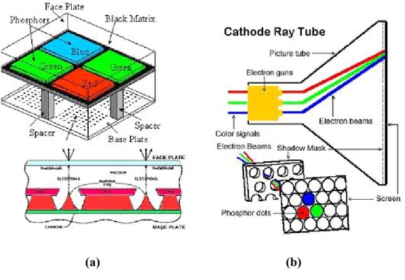
Fig. 1-2 The schematic diagram of (a) field emission arrays (FEAs), (b) conventional cathode ray tube (CRT)
Fig. 1-3 Energy diagrams of vacuum-metal boundary: (a)without external electric field; and (b) with an external electric field
Fig. 1-4 The SEM micrograph of (a) Spindt type triodes array, (b) Spindt type field emission triode, and the schematic image of (c) Spindt type triode diagram Fig. 1-5 The SEM images of (a) pyramidal structures formed by wet etching, (b)the
silicon tips formed by SF6 plasma etching ,(c) silicon tips sharpened by thermal oxidation.
Fig. 1-6 The FED products based on Spindt type field emitters, (a) motorola 5.6” color FED, (b) Pixtech 15” color FED, (c) Futaba 7” color FED and (d) Sony/Candescent 13.1” color FED
Fig. 1-7 This diagram is the field emission mechanism of BSD.
Fig. 1-8 (a) The SCE top view , (b) the field emission operation diagram of SCE. Fig. 1-9 Structures of carbon (a) graphite, (b) diamond, (c) fullerene
Fig. 1-10 TEM images of (a) SWNT, and (b) MWNT
Fig. 1-11 Growth mechanism of CNTs growth (a) base growth model, (b) tip growth model
Fig. 1-12 Heat of formation of various hydrocarbon gases.
Fig. 1-13 (a) Schematic diagram of the thermal CVD system employed for carbon nanotube growths. At the center is a boat served as the substrate holder. A thermocouple is directly inserted inside the quartz tube near the substrate to
monitor the gas temperature. (b) The standard pretreatment and growth conditions employed for carbon nanotube growths.
Fig. 1-14 Schematic diagram of the CVD system for the growth of CNTs at low temperatures.
Fig. 1-15 The growth rate variation with temperature for thermal CVD and PECVD. The data points for thermal CVD and high temperature PECVD are from previous data by Ducati et al.. The values for the activation energies were calculated from a linear interpolation of the slopes.
Fig. 1-16 Lindemann criterion [2.26]
Fig. 1-17 The figure shows melting point relationship about Fe thin films on Al2O3.
Fig. 1-18 SEM and phosphor emission images of gated FEAs taken at the samples with the Al and catalyst thickness of (a) 2/2, (b) 5/2, and (c) 2/5 nm. Emission images and current–voltage curves were observed at the gate voltage of 60 V with 1/240 duty and the anode voltage of 1 kV. Emission current versus gate voltage curves of each gated FEAs are in (d). [2.32] Fig. 1-19 (a) Simulation of the e- potential lines of the electrostatic field for tubes of 1
mm height and 2 nm radius, for distances between tubes of 4, 1, and 0.5 mm; along with the corresponding changes of the field enhancement factor β and emitter density (b), and current density (c) as a function of the distance.
Fig. 1-20 two kinds of triode structure (a) Top Gate structure (b) Bottom Gate structure
Fig. 1-21 the relationship between melting point and particle sizes….Co metal for example [2.40].
Fig. 1-22 In-situ TEM images recorded from a region of capped Pt nanocrystals at various specimen temperatures. Surface diffusion or surface premelting of
nano-size particles takes place when the temperature is raised above 500ْ C. [2.41]
Fig. 1-23 The schematic diagram for the CNT growth using multilayer catalysts. (a) Multilayer deposition, (b) Catalyst particles formation after pretreatment, and (c) CNT growth.
Chapter 2
Fig. 2-1 Schematic experimental procedures
Fig. 2-2 A (a) photo and (b) schematic picture of thermal CVD
Fig. 2-3 Diode structure fabrication flow diagrams (a) 2000A Cr cathode deposition by Egun, (b) Lithography procedure (c) Multilayer catalysts deposition, (d) Lift photoresist off, (e) Pretreatment, and (f) CNT growth.
Fig. 2-4 Triode structure fabrication flow diagrams
(a) 2000A Cr cathode, 1um SiO2, and 2000A Cr gate deposition by Egun,
PECVD, and Egun, respectively. (b) Lithography procedure, (c) Define the gate and spacer by wet etching, (d) Multilayer catalysts deposition, (e) Lift photoresist off, (f) Pretreatment, and (g) CNT growth.
Fig. 2-5 Diode structure of CNT-FED on glass substrate
(a) 2000A Cr cathode deposition by Egun, (b) Lithography procedure (c) Multilayer catalysts deposition, (d) Lift photoresist off, (e) Pretreatment, and (f) CNT growth.
Fig. 2-6 High vacuum measurement system
Chapter 3
Fig.3-1 After pretreatment in Exp. A
(a) 20Co/20Cr , (b) 20Co/100Al ,(c) 20Co/20Cr/20Al , (d) 20Co/20Cr/50Al , (e) 20Co/20Cr/100Al , and (f) 20Co/20Cr/200Al
Fig.3-2 SEM cross-section images of CNT growth in Exp. B and inset image represents the top view image of each one.
(a) 20Co/20Cr/20Al , (b) 20Co/20Cr/50Al , (c) 20Co/20Cr/100Al , and (d) 20Co/20Cr/200Al
Fig.3-3 Raman analysis in Exp. B ; G peak at 1580 cm-1 and D peak at 1350 cm-1 Fig.3-4 (a) TEM analysis in the Exp. B and (b) EDS analysis in the Exp. B
Fig.3-5 (a) I-V plot in the Exp. B and (b) F-N plot in the Exp. B
Fig.3-6 SEM cross-section images images of CNT growth in Exp.C and inset image represents the top view image of each one.
(a) 20Co/20Cr/100Al , (b) 20Fe/20Cr/100Al , and (c) 20Ni/20Cr/100Al Fig.3-7 (a) I-V plot in the Exp. C and (b) F-N plot in the Exp. C
Fig.3-8 The luminescent image of CNTs (1mm x 1mm) using 20Co/20Cr/100Al at 6.25 V/um in Exp. C
Fig.3-9 The luminescent image of CNTs (1.0cm x 1.5cm) using 20Co/20Cr/100Al in Exp. C (a) E=2.5 v/um (b) E=3.75 v/um (c) E=5.0 v/um (d) E=6.75 v/um Fig.3-10 SEM cross-section images images of CNT growth in Exp. D and inset image
represents the top view image of each one.
(a)20Co , (b) 20Co/100Al , (c) 20Co/10Cr/100Al , (d) 20Co/20Cr/100Al, and (e) 20Co/50Cr/100Al.
Fig.3-11 XRD analysis for CNTs using 20Co/10Cr/100Al in Exp. D
Fig.3-12 SEM cross-section images of CNT growth in Exp.E and inset image represents the top view image of each one.
(a) 10Co/20Cr/100Al , (b) 20Co/20Cr/100Al , (c) 50Co/20Cr/100Al, and (d) 100Co/20Cr/100Al.
Fig.3-13 (a) I-V plot in the Exp. D,E and (b) F-N plot in the Exp. D,E
20Co/20Cr/100Al (a) 500ْْ C, (b) 550ْْ C , (c)600ْْ C, and (d) 650ْْ C. Fig.3-15 (a) I-V plot in the Exp. B,F,G,H and (b) F-N plot in the Exp. B,F,G,H Fig.3-16 TEM analysis of CNT growth in Exp.B,F,G,H using 20Co/20Cr/100Al
(a) 500ْْ C, (b) 550ْْ C , (c)600ْْ C, and (d) 650ْْ C.
Fig.3-17 EDS analysis of CNT growth in Exp.B,F,G,H using 20Co/20Cr/100Al (a)500ْْ C, (b) 550ْْ C , (c)600ْْ C, and (d) 650ْْ C.
Fig.3-18 Arrhenius plots for CNT Growth rates versus 1/T in Exp. B,F,G,H
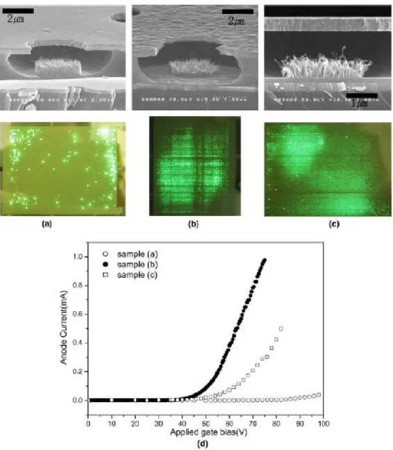
Fig.3-19 SEM images of CNT growth with Triode structure using 20Co/20Cr/100Al (a) in the Exp. B, (b) in the Exp. I, and (c) in the Exp. J
Fig.3-20 (a) Jg-Vg plot at Va=1000v in the Exp. I , (a) Ja-Vg plot at Va=1000v in the Exp. I , and (c) Ja-Va plot at Vg=0 in the Exp. I
Fig.3-21 (a) Jg-Vg plot at Va=1000v in the Exp. J , (a) Ja-Vg plot at Va=1000v in the Exp. J, and (c) Ja-Va plot at Vg=0 and Vg=50v in the Exp. J
Fig.3-22 SEM images of CNT growth on the glass substrate in Exp. K using 20Co/20Cr/100Al
Chapter 1
Introduction
1.1 Overview of Vacuum Microelectronics
1.1.1 History of Vacuum Microelectronics
During the World War 2 (1939-1945), Dr. Mauchly and Eckert designed vacuum tubes in place of relays for the motion of an artillery projectile. Although the first generation computer had the fast operation speed, its computer occupied the huge space (1500ft2) and wasted most electricity. In addition, the vacuum tube was very fragile. In 1948, the first semiconductor transistor was invented by Bardeen, Brattain, and Shockley [1.1], and integrated circuits were subsequently developed in the 1960s [1.2]. This was a great revolution of the electrical applications from vacuum tubes to semiconductor transistors. People generally thought that the time of using vacuum tubes was over. Gradually, vacuum tubes were replaced by solid state electronic devices due to their tiny volume, low cost, better reliability, and high power efficiency. In the past decades, the semiconductor manufacturing technology from SSI to ULSI had a great improvement. Then, this mature technology gave a new life to vacuum electronics for the professional micro fabrication process to fabricate tiny vacuum devices, which is now called vacuum microelectronics. “Vacuum state” devices have a great deal of superior advantages as compared with solid-state devices, including fast carrier drift velocity, radiation hardness, and temperature insensitivity. Investigation on Table 1.1 that compares the characteristics of vacuum microelectronic devices with semiconductor devices, it becomes quite clear that vacuum state is a vastly superior transport medium compared to solids. The
electron velocity in vacuum can approach the speed of light (3 × 1010 cm/s), while the saturation velocity in solid state devices is typically limited to 107 cm/s by collisions with optical and acoustic phonons [1.3]. Therefore, various forms of electron-beam devices can by taking advantage of vacuum as the electron transport medium, and electro-components such as lenses, reflectors, and deflectors can also be made. Furthermore, temporary or permanent radiation effect is negligible in vacuum devices for no medium being damaged. Additionally, the effect of temperature on performance is reduced in vacuum devices simply for no medium causing the temperature effect in semiconductor, such as increased lattice scattering or bulk carrier generation/recombination.
In order to accomplish better understanding of the advantages of vacuum microelectronics, a brief history of the field emission theory and vacuum microelectronic devices is necessary. Recent developments in vacuum microelectronics started in 1928 when R. H. Fowler and L. W. Nordheim published the first theory of electron field emission from metals using quantum mechanics [1.4]. Charbonnier had given a clear description of the transition from field emission to thermionic emission [1.5]. Fowler-Nordheim theory was different from thermionic emission, which metal has to be heated so that some of the electrons in the metal gain enough thermal energy to overcome the metal/vacuum barrier; according to the Fowler-Nordheim theory, an applied electric field of approximately 103 V/µm is needed for electrons to tunnel through the sufficiently narrow barrier [1.4]. In 1961, K. R. Shoulders first published the investigation on field emission sources based on the Fowler-Nordheim theory [1.6]. In 1968, C. A. Spindt successfully contributed the semiconductor technology to the vacuum microelectronics, called the Spindt-type cold cathode [1.7]. Since the Spindt-type triode came up, many scholar and scientists devoted their innovation to its field emission field. In 1972, R. N. Thomas and H. C. Nathanson brought up the new Spindt type made of silicon [1.8]. For the better field emission characteristics, scientists wanted to enhance emission
currents by coating different metals, such as W, Mo, Ta, Pt etc., even diamond on field emission arrays [1.9-1.11]. Then, in the past 30 years, field emission cold cathode materials became a promising technology and hundreds of research organizations devoted their money and innovation to its field emission applications.
1.1.2 Application of Vacuum Microelectronics
Due to the superior properties of vacuum microelectronic devices, potential applications had been invented, including high brightness flat-panel display [1.12-1.16], high efficiency microwave amplifier and generator [1.17-1.19], ultra-fast computer, intense electron/ion sources [1.20-1.21], scanning electron microscopy, electron beam lithography, micro-sensor [1.22-1.23], temperature insensitive electronics, electrom/ion souces, excitation sources, and radiation hardness analog and digital circuits.
Among wide range applications of the vacuum microelectronics, flat-panel display exhibits superior advantages inclusive of super thin panel, high brightness, high contrast, large view angles, high response speed, low driving voltages, low power consumption, and a self-luminary. Most importantly FPD can be operated in the worst environment compared to the solid state electronics. Fig 1-1 showed the applications of flat panel display.
Various kinds of flat-panel displays can be classified into two groups: Emissive and Non-Emissive type. Liquid crystal display (LCD) belongs to the Non-Emissive type. However, organic light emission display (OLED), vacuum fluorescent display (VFD), plasma display panel (PDP), and field emission display (FED) belong to the Emissive type. They all were developed for the better characteristics of small volume, light weight, and low power consumption.
between liquid crystal, environment temperatures, and operation voltages. Second, low brightness and high costs arise from the backlight model. Last, the view angle is not large. However, based on the mature semiconductor technology, LCDs are most popular displays in the world. OLEDs have many advantages, such as no needs for the backlight model, low cost, low power consumption, high view angles, high contrast, and high response speed. Most importantly OLEDs can be fabricated to be a full color and large scale panel, even for the flexible panel applications. But, OLEDs should overcome the worst drawback “short life time”. The theory of luminesce of FEDs is very similar to the Cathode Ray Tube (CRT). The cathode of CRT generates thermionic electrons by heating, then offset voltages accelerate and concentrate the electrons, then the magnet controls the direction of electrons, and electrons scan the phosphor back and forth. The anode of FED can be applied at suitable turn-on electrical field and the cathodes emit electrons based on the FN tunneling. FED features all the pros of the CRTs in image quality and possesses flat and small volume. The schematic comparisons were revealed in Fig.1-2.
As the all of the above saying and the Table 1.2, FEDs possess the advantages, such as low weight and small volume, high brightness, high contrast, large view angles, high response speed, low driving voltage, low power consumption, self-emission, and normal operation in the worst environment. But, some critical issues should be overcome like short life time, uniformity and stability of emission currents, and vacuum package. However, in the display field, LCDs and PDP still dominate the market of the small and large panel display, respectively. With the revolution and innovation of new technology, we believe FEDs will be a promising display in the future.
1.2.1 Theory Background
Field emission theory had been investigated for hundreds of years. In 1897, R. H. Wood found metals or semiconductors could emit electrons at high electrical field (109v/m). In 1928, R. H. Fowler and L. W. Nordheim published the first theory of electron field emission from metals using quantum mechanics [1.4].
Electron field emission is a quantum mechanical tunneling phenomenon of electrons extracted from the conductive solid surface, such as a metal or a semiconductor, where the surface electric field is extremely high. If a sufficient electric field is applied on the emitter surface, electrons will be emitting through the surface potential barrier into vacuum, even under a very low temperature. In contrast, thermionic emission is the hot electron emission under high temperature and low electric field. Fig. 1-3(a) demonstrated the band diagram of a metal-vacuum system.
Here W0 is the energy difference between an electron at rest outside the metal and an
electron at rest inside the metal, whereas Wf is the energy difference between the Fermi level
and the bottom of the conduction band. The work function φ is defined as φ = W0 - Wf. If an
external bias is applied, vacuum energy level is reduced and the potential barrier at the surface becomes thinner as shown in Fig. 1-3(b). Then, an electron having energy “W” has a finite probability of tunneling through the surface barrier. Fowler and Nordheim derive the famous F-N equation (1.1) as follow [1.4]:
( )
exp[ 2 ( )/ ] 3 2 2 E y v B y t AE J φ φ − = , (1-1)where J is the current density (A/cm2). E is the applied electric field (V/cm), φ is the work function (in eV), A = 1.56×10⁻⁶, B = -6.831×10⁻⁷, y = 3.79x10-4×10-4E1/2/φ, t2(y)~1.1 and
), 5 . 0 cos( ) (y y v = π (1-2) or . 95 . 0 ) ( 2 y y v = − (1-3)
Typically, the field emission current I is measured as a function of the applied voltage V. Substituting relationships of J = I/α and E = βV into Eq.(1-1), where α is the emitting area and β is the local field enhancement factor of the emitting surface, the following equation can be obtained ] ) ( exp[ ) ( 2 3 2 2 2 V y Bv y t V A I β φ φ αβ − = . (1-4) Then taking the log. form of Eq. (1-4) and v(y) ~ 1
) ) ( ( 10 97 . 2 ] ) ( 10 54 . 1 log[ ) log( 2 3 7 2 2 6 2 V y v y t V I β φ φ αβ − × × = − , (1-5)
from Eq. (1-5), the slope of a Fowler-Nordheim (F-N) plot is given by
) ( 10 97 . 2 2 3 7 β φ × − = ≡slopeFN S , (1-6)
The parameter β can be evaluated from the slope S of the measured F-N plot if the work function φ was known
) ( 10 97 . 2 2 3 7 S φ β =− × (cm-1), (1-7) The emission area α can be subsequently extracted from a rearrangement of Eq. (1-5)
) 10 53 . 6 exp( ) 89 . 9 exp( 10 4 . 1 ) ( 2 3 7 2 6 2 V V I β φ φ β φ α − × × = − (cm2). (1-8)
For example, the electric field at the surface of a spherical emitter of radius r concentric with a spherical anode (or gate) of radius r+d can be represented analytically by
) ( d d r r V E= + , (1-9)
Though a realistic electric field in the emitter tip is more complicated than above equation, we can multiply Eq.(1-9) by a geometric factor β ` to approximate the real condition.
≡ tip E function of (r,d) =β ` ( ) d d r r V + , (1-10) where r is the tip radius of emitter tip, d is the emitter-anode(gate) distance and β ` is a geometric correction factor [1.25].
For a very sharp conical tip emitter, where d >> r, Etip approaches to β `(V/r). And for
r>>d, Etip approaches to β `(V/d) which is the solution for a parallel-plate capacitor and for a
diode operation in a small anode-to-cathode spacing. As the gated FEA with very sharp tip radius, Eq. (1-10) can be approximated as:
Etip =β `(V/r). (1-11)
Combining E= β V and Eq. (1-11), we can obtain the relationship:
Etip =β V = β `(V/r), and β `= β r. (1-12)
The tip radius r is usually in the range from a few nm to 50 nm, corresponding to the parameter β ` ranging from 10-1 to 10-2.
Besides, transconductance of a field emission device is defined as the change in anode current due to a change in gate voltage [1.3].
m g g C m V I g ∂ ∂ = |Vc , (1-13)
of current charge that can be accomplished by a given change in grid voltage. The transconductance can be increased by using multiple tips or decreasing the cathode-to gate spacing for a given cathode-to-anode spacing.
According to the equations above mentioned (especially Eq.1-5), the following approaches may therefore be taken to reduce the operating voltage of the field emission devices:
(1) Find methods to increase the aspect ratio of emission cathodes (increaseβ ). (2) Lower the work function of the tip (φ )
(3) Narrow the cone angle (increaseβ ).
(4) Reduce the gate-opening diameter (increaseβ ). (5) Increase the emission sites.
1.2.2 Cold Cathode Structures and Materials for Field Emission Display
With the improvement on the semiconductor fabrication technology, FED is one of the most promising applications of flat panel displays, which can overcome the drawbacks of TFT-LCD. The features of FEDs are small volume, low power consumption, fast response speed, color performance similar to CRT, large view angles, and low cost. Otherwise, FEDs have some drawbacks, such as the uniformity of brightness, high breakdown voltage, the package spacer charging, short life time, and vacuum package, which are all serious problems. In the past 30 years, so many applications of FEDs were demonstrated by the academia and noted laboratories. Table 1.3 showed the comparison of the FEDs. Based on the emitting methods, we could separate the FEDs into two groups: direct and fractional emitters. The CNTs and Spindt type can emit electrons directly from the emitters, so they belong to the
direct emitters. Moreover, the BSD, MIM, and SED emit electrons form dispersed nano-particles of the thin films, and they belong to the fractional emitters.
A. Spindt-Type Field Emitters
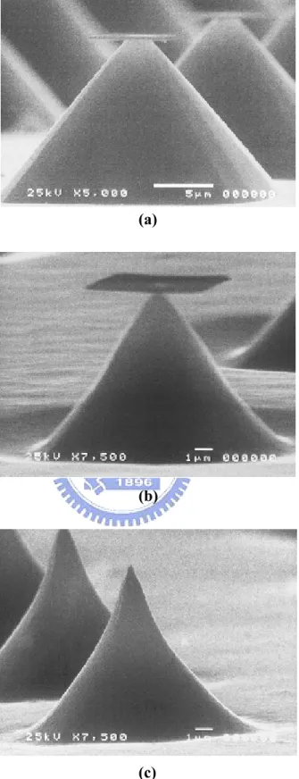
Since 1960s, the concepts of FEDs were demonstrated, and many scientists contributed their innovation to the FED applications. Ken Shoulders published the first micro-electric device based on the F-N tunneling theory [1.26]. However, Capp Spindt who successfully fabricated and operated the FEA (Field Emission Array) contributed the semiconductor technology to the vacuum microelectronics, called the Spindt-type cold cathode [1.7]. The Spindt-type is micro-meter scale emitters and possess self aligned metal pyramids and gates [1.27]. The Fig 1-4 was Spindt-type triode structure fabricated by Capp Spindt. From then on, many applications of FEDs were demonstrated by the academia and noted laboratories. The Spindt-type has some advantages, such as high thermal stability, high emission reliability, low cost, and larger area displays of many tip arrays. In addition, the most importance is Spindt-type can be easily fabricated in the general semiconductor fabrication technology.
However, the most popular Spindt-type material is silicon tip emitters. Fig 1-5 is silicon tip diagrams. The most desirable characteristics of silicon tips are the low operation voltage, emission stability, long durability, and high emission current density. These properties are strongly dependent on the tip curvature radius (related to the field enhancement factor), emission material (determines the work function), and surface conditions. According to Eq.(1-1), the methods to enhance the emission currents are increasing the work function of cathode materials and increasing the field emission factor (β). We had to decrease the work function of silicon tips and coat conduction layers, such as DLC (Diamond Like Carbon), carbon films, Mo….etc [1.9-1.11,1-29]. Conduction layers can decrease the silicon work function and enhance the emission efficiency. However, there are some existing drawbacks of Spindt type field emitters when fabricating Spindt type FED such as (1) high gate driving
voltage required; for a Spindt type field emission triode with 4 µm gate aperture, the driving voltage is typically more than 60 V, which results in the high cost of the driving circuits. To reduce the gate driving voltage, (1) frontier lithography technologies such as E beam lithography must be applied to reduce the gate aperture to the sub-micron level and (2) huge and expensive high vacuum deposition system is required during fabricating large area Spindt type FED.
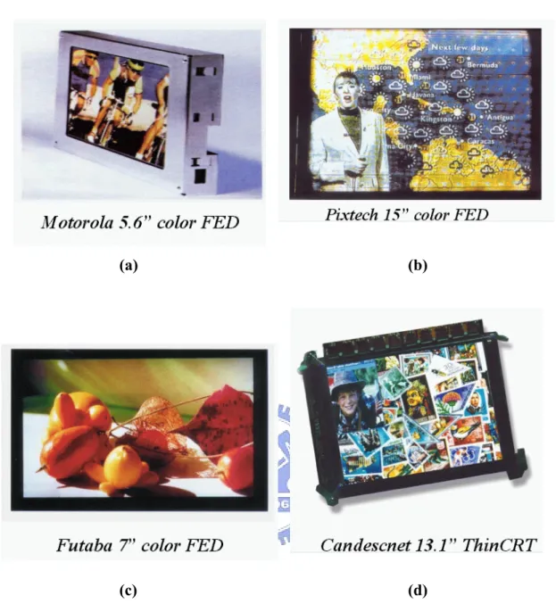
Some research groups had successfully fabricated commercial FED products based on Spindt type field emitters such as Futaba, Sony/Candesent, Futaba and Pixtech[1.30], the products above mentioned companies were shown in Fig.1-6.
B. BSD Field Emitters
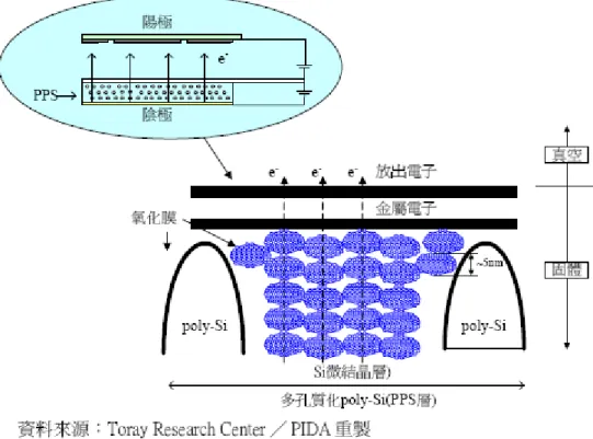
BSD (Ballistic Electron Surface Emitting Device) was developed by Panasonic and Tokyo University of Agriculture and Technology. The operation diagram of BSD was showed in the Fig 1-7. The PPS (porous poly-Si) of cathodes of BSD have micro-crystal particles, which have a thin oxide film on itself. The offset voltages are applied between the anode and cathode, the electrons emitted by the cathode inject into the PPS, the electrons accelerated by the PPS interactions gain high energies and emit, and the emission efficiency of electrons is about 2%. Because the external voltages are focused on the oxide surface of the micro-crystal particles, then the thin film surface forms strong electrical fields, and the electrons can be emitted. However, the phenomenon called “Ballistic Electron Conduction”. In addition, the high active electrons are emitted from the cathode in the vertical direction without the deviation adjustment. The BSD has the advantages, such as simple structures, but it is very sensitive to the ion bombardments and has serious drawbacks like the poor emission efficiency.
MIM (Metal Insulator Metal) technology was investigated by Hitachi and LGE, but they didn’t publish the detailed technology researches. According to the paper survey, MIM technology is the hot electron generation in the dielectric. The features of MIM are the low degrees of electron dispersion, low driving voltages, and high current density, but it is easily affected by the ion bombardments. However, the structure and fabrication of MIM are very complicated.
D. SCE Field Emitters
Canon and Toshiba co-operated the whole new 36 inches planar panel display called “SCE (Surface Conduction Emitter)” and published a plan for large productions in Sep 14 2004 [1.31]. Fig 1-8 was the base structure of SCE. At SID 2005, Canon showed the SCE display specifications, including 400 cd/m2
peak luminance, high contrast about 10000:1, response speed below 1ms, and panel thickness about 7.3mm. By the way, it showed the superior emission stability
As the Fig 1-8, the mechanism of emission of SCE is the external voltage is applied on the PdO particles located in the extreme narrow gaps, the electrons emit from the extreme narrow gaps based on tunneling effect, and electrons hit onto the phosphors of anodes. Moreover, the PdO thin film was coated by the ink-jet methods, and its thickness was about 10nm. The currents passed through the PdO thin film and about 2% electrons emited into the vacuum. Its emission efficiency compared to other field emission emitters is much better. The features of SCE are the simple structure, low cost and large panel display. But, in accord with the other FEDs, some essential properties like stable emission currents, low driving voltages, low cost fabrications, and longer operation life are still needed to be resolved.
Since the discovery of carbon nanotubes (CNTs) by Iijima in 1991, [1.32] CNTs have attracted considerable interests because of their unique physical properties and many potential applications [1.33]. CNTs have numerous potential applications in nanoelectronics, nanometer-scale structural materials, hydrogen storage, field-emission devices, and so on. Among these applications, CNTs seem to be very promising as electron emitters for field-emission displays (FEDs).
1.3.1 Structures of Carbon Nanotubes
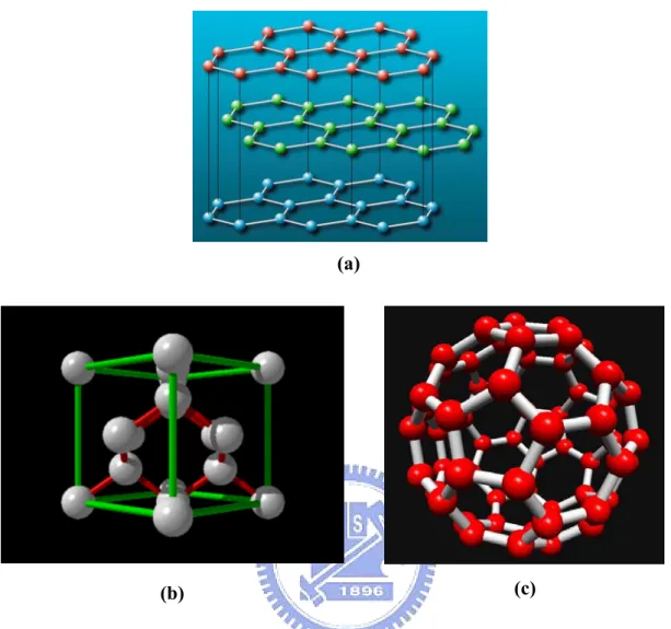
Carbon nanotubes are cylindrical molecules consisting of single or multi-graphite layers. Unlike other covalent matters, carbon shows various structures. The common allotropes of carbon are (1) graphite, (2) diamond, and (3) fullerene (Fig. 1-9). Among them, graphite is a planar structure of carbon in sp2 bonding. As the scale of graphite is close to the nano scale, it could curl and form a hollow tube. According to the number of layers in the tube wall, we classify the carbon nanotubes into two kinds: (1) single-walled (SWNTs) and (2) multi-walled carbon nanotubes (MWNTs) (Fig. 1-10).
A. Single-walled Carbon Nanotubes
The curling direction of graphite decides the characteristics of single-walled carbon nanotubes, like metal or semiconductor. Based on the curling direction, we can classify SWNTs into three kinds: (1) armchair, (2) zigzag, (3) chiral. The armchair SWNTs reveal metallic property. The zigzag and chiral SWNTs possess both of metallic and semiconductor properties.
B. Multi-walled Carbon Nanotubes
every layer may be different. MWNTs present different morphology by various growing parameters. In terms of appearance, we can approximately categorize MWNTs into several types: (1) standard tube, (2) spiral, and (3) “Y” model. If we further investigate the microstructure of the MWNTs, we can observe that there are different structures such as hollow-liked, bamboo-liked and fish-bone-liked MWNTs.
1.3.2 Physical and Chemical Properties of Carbon Nanotubes
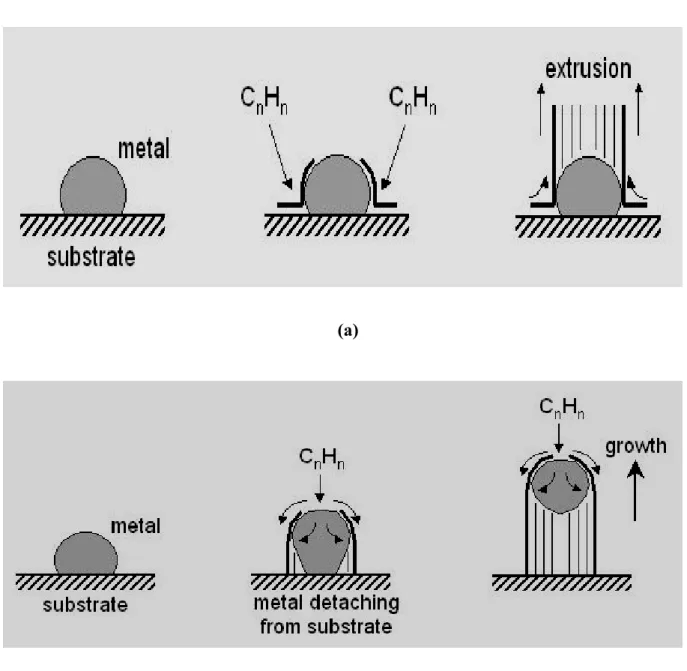
Carbon nanotubes have several superior characteristics, such as high thermal conductivity (2000 W/m.K), good heat resistance, low chemical reactivity, and high aspect ratio [1.34]. These properties are suitable for a field-emission source. In addition, carbon nanotubes have an excellent mechanical property, especially for the high Young modulus about 1.25T Pa [1.35]. But, CNTs have drawbacks, such as semiconductor/metal types [1.36], and uniformity growth issues. As the Fig 1-11, carbon nanotubes growth can be classified into two types: tip growth model and base growth model. There are many explanations about carbon nanotubes growth mechanism. Generally speaking, the growth mechanism is VLS (Vapor Liquid Solid). First, catalyst films transform to the particles because of thermal force or plasma. Formation of catalyst particles enhances the diffusion of carbon in the metal alloy. Second, the hydrocarbon precursors are decomposed from the reaction gases and carbon sources dissolve into the catalyst particles until the carbon saturation. Finally, carbons diffuse from the catalyst center to its surface and precipitate to form carbon SP2 bonding. Then,
through the VLS, we can synthesize the carbon nanotubes.
1.3.3 The Synthesis Methods of Carbon Nanotubes
discharge, laser vaporization, pyrolysis, solar energy, and plasma-enhanced chemical vapor deposition (CVD), for its unique physical and chemical properties and for applications to nanoscale devices. However, common methods of CNT synthesis include: (1) arc-discharge [1.37], (2) laser ablation [1.38], (3) thermal CVD [1.39-1-41], and (4) plasma enhanced CVD [1.42-1-43].
The laser ablation can synthesize pure carbon nanotubes in high fabrication temperature, but large scale display panel can not be fabricated in the high fabrication temperature above the melting point of glass substrate. The arc discharge can synthesize carbon nanotubes in shorter fabrication times, but it has some issues, such as (1) poor purity, (2) hard to control growth orientations of carbon nanotubes, and (3) poor emission uniformity. Compared to laser ablation and arc discharge, using CVD for carbon nanotube growth has some features, such as (1) high purity carbon nanotubes, (2) selective growth only for catalyst metal, (3) controlling growth direction, and (4) much suitable to semiconductor fabrication procedure. However, with the display technology trend, it is the time for large panel display. We need to synthesize carbon nanotubes using CVDs on large panel substrates. For this reason, carbon nanotube growth at low temperatures is unavoidable, but the purity of carbon nanotubes at low temperatures is poor. So, we still try some methods to increase growth rates at low temperatures, such as (1 ) multilayer catalysts, (2) plasma CVDs, (3) post-treatment, and so on.
1.3.4 Applications of Carbon Nanotubes
Since the discovery of CNTs in 1991, CNTs had attracted much attention for their unique physical and chemical properties. Their extensively potential applications lead them to become a super star of nano technology, which cover: (1) Chemical sensor [1.44], (2) IR
detector, (3) Nano-conducting Wire, (4) Vehicles for Hydrogen Storage [1.45], (5) Field Effect Transistor [1.46], (6) Field Emission Display (FED), (7) Probe of AFM and etc.
In the wide-ranging applications of CNTs, FED arouses researchers’ interest particularly. In virtue of the superior field emission characteristics, CNTs are applied to the emitting source of cold cathode. The advantages of FED are its low response time, wide view angle, high brightness, high working temperature range and well combination with mature phosphor technology. However, a major problem needs to be solved in this field. It is not allowed to effectively analyze CNTs on a flat panel at relatively lower temperature (<500°C) and this barrier restriction obstructs the development of CNT-FED so far.
1.4 Paper Review
1.4.1 Overview of CNTs Growth at Low Temperature
Carbon nanotubes are the most important materials for field emission displays (FED) due to their superior emission characteristics as described in the previous section 1.3. Therefore, CNTs are attributed to be one of the most attractive of potential field emitters for flat-panel displays. How to synthesize high purified carbon nanotubes is a great challenge. Some critical factors like catalyst metals, hydrocarbon gases, and growth methods extremely affect CNT growth.
Various synthetic methods such as arc discharge [1.47], laser vaporization [1.48], pyrolysis, and plasma-enhanced [1.49-1.51] or thermal chemical vapor deposition CVD [1.52-1.53] were employed. Synthesis of well-aligned CNTs on a large area is necessary for one of various applications, electron emitter of field emission displays. The arc discharge and the laser vaporization techniques can produce the large amount of CNTs, but it is very difficult to control the alignment and size. These techniques also require purification process
to separate pure CNTs from other particles. Many research groups have employed the CVD method for the purpose of large scaled production of CNTs. It is shown that the CVD technique can synthesize the CNTs with high purity, high yield, selective growth, and good vertical alignment.
The synthesis of carbon nanotubes can be divided into non-catalytic and catalytic methods. In the catalytic method, nickel, iron and cobalt are the only three transition metals that can be used as pure-metal catalysts for carbon nanotube growth. In the considerable reports regarding carbon nanotube synthesis, nickel, iron and cobalt are used either separately in different methods or together as a composite catalyst. The study clearly shows that the catalyst strongly influences not only diameter, growth rate, etc., but also morphology and microstructure [1.54]. In the growth reaction of CNTs, the diffusion of carbon in the catalyst metal has been believed to be the rate-determining step. We also know that the solubility of carbon in a metal is temperature dependent [1.55-1.56]. As theTable 1.4, Fe, Co, and Ni are the most suitable catalyst metals compared to other metals for the CNT growth.
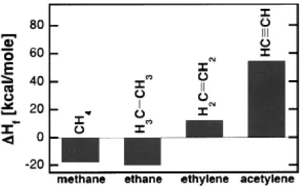
According to researches by Siegal et al., four hydrocarbon gases were studied: C2H2,
C2H4, and C2H6, which have a C–C triple, double, and single bond, respectively, and CH4
[1.57]. The chemical reactivity of these compounds is related to their heats of formation, obtained from the CRC Handbook of Physics and Chemistry, and shown in Fig. 1-12. In general, the greater bond numbers, the more reactive. Therefore, the reactivity is C2H2>
C2H4> C2H6. With negative heats of formation, both ethane and methane are the least reactive,
with ethane slightly less than methane.
Molecular dynamic simulation results using a potential energy surface method had been published by Ding et al. [1.58] showing that these iron clusters must reach supersaturated carbon levels before nanotube formation begins. This saturation had also been described by Kuznetsov with the use of phase diagrams [1.59]. The rapid diffusion of carbon in iron
allowed for rapid carbide formation and quick graphite precipitation. With cobalt and nickel, meta-stable carbides (Co3C, Co2C, and Ni3C [1.60]) formed immediately following saturation of carbon in the solid solution, and as additional carbon diffuses into the catalyst, graphite precipitates out, forming a nanotube. Furthermore, carbide formation inhibited nanotube growth from the pure metal, carbides could be used as potential catalysts to encourage graphite precipitation, provided the carbide particles were appropriately sized and carbon diffusion was sufficiently fast. For optimal growth in typical chemical vapor deposition, metal catalysts need to exhibit (1)sufficient carbon solubility, (2)rapid carbon
diffusion, and (3)limited carbide formation[1.61]. Table 1.5 was summarized for the many
kinds of carbide formation.
Considering the direct growth of CNTs on the substrate, thermal CVD is often used because the damage to the substrate is small. The reaction temperature of thermal CVD is generally higher than 700℃ in earlier experiments. There are two critical purposes to grow CNTs at higher temperature. One is to gain uniform catalyst nano-particles after pretreatment, and the other is to obtain fine graphite structure of CNTs.
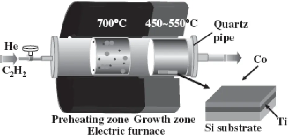
Recently, the direct growth of CNTs on glass substrate by thermal CVD at low temperature has been researched for the fabrication of field emission displays. For practical application, soda lime glass is one of the most preferable materials for the cathode substrate of filed emission displays because of its cheapness. Although using soda lime glass substrate indeed costs down, the melting point of 570℃ restricts the processing temperature when growing CNTs by thermal CVD. Some methods like (1) external treatments or (2) two-stage thermal CVD are employed to enhance CNT growth at low temperature. Yih-Ming Shyu et al. synthesized CNTs using Fe-Ni alloys by the thermal CVD at 400ْC [1.62-1.63]. As the Fig. 1-13, they introduced C2H2 into the pre-treatment region in order to increase carbon solubility
Takeda et al. had found that preheating the reaction gas C2H2 at 700℃ enhanced its reactivity
and contributed to the effective decomposition of the gas on the surfaces of catalyst particles heated even at 450℃ [1.64-1.65]. They could synthesize high graphite CNTs even better than CNT grown at high temperature by two stage temperature zones. Plasma-enhanced CVD is also the popular method for the CNT growth because plasma energy compared to thermal CVD (Fig. 1-15) can more effectively decompose catalyst metals to form the particles [1.66-1.68]. So, its methods are more suitable to CNT growth at low temperature. But, it still has drawbacks, including plasma damages to substrates, vacuum operation, high cost, and non-uniformity issues. For a summary, thermal CVD is most promising method for CNT growth.
1.4.2 Theoretical Background for CNTs at Low Temperature
1.4.2.A Effects of Catalyst Film Thickness on The Melting Point
The most importance for CNT growth is low temperature fabrication. As described in the previous section 1.4.1, there are so many methods to be employed for the low temperature fabrication. However, if we could effectively lower the melting point of catalyst metals, we would grow CNTs at much lower temperature and did not damage the graphite quality of CNTs. For examples, Takagi in 1954 [1.69] demonstrated for the first time that ultrafine metallic particles melt below their corresponding bulk melting temperatures. Moreover, the metallic nanocrystals could exhibit not only melting point depression, but also superheating, depending on their surrounding environment. When the thickness of a thin film reaches monolayer level, the thin film may melt at a much lower temperature than its bulk melting point. Recently, a model, free of any adjustable parameter, for the size-dependent melting for nanocrystals was introduced by the use of Mott’s expression for the vibrational entropy of
melting [1.70] and the Lindemann’s criterion for melting [1.71]. In light of Lindemann criterion, the melting point decreases abruptly when the catalyst was close to nano-sizes (Fig 1-16). Q. Jiang et al. investigated several thin films, including Pb, In, Sn, and Fe thin films [1.72]. As the Fig 1-17, taking the Fe for examples, and we can find out that the melting temperature of a crystalline thin film decreases as its thickness decreases. In other paper survey [1.73-1.74], they investigated the surface tension between the catalyst thin films and substrates and also proposed the same result on the lower melting point as the thin film thickness decreased.
1.4.2.B Effects of Buffer Layers on CNT Growth
The use of buffer layers between catalyst and silicon substrate in growth of carbon nanotubes by chemical vapor deposition (CVD) has the two effects of both increasing the efficiency of the growth process by avoiding undesired chemical interaction between catalyst and substrate, and of altering the catalyst-support interaction, therefore modifying the characteristics and growth rate of CNTs. In sum, using good buffer layers can effectively make catalyst films form the catalyst particles without merging together and control the CNT density as its thickness increases. In the paper surveys, the comparative efficiency of buffer layers of Al, Al2O3, TiN and TiO2 in the CVD growth of CNTs was investigated [1.75-1.76].
Making use of an experimental setup for CNT growth combined with in situ photoelectron spectroscopy analysis, we found that CNTs did not grow whenever pure Al layers were employed, in opposition to the results published by Delzeit et al.. However, when we used the corresponding oxide Al2O3 as buffer layer CNT growth was successful. Furthermore, Al2O3
layers did indeed promote formation of thinner nanotubes as compared with other buffer layers like TiN or TiO2 [1.77-1.78]. In particularly, In Taek Han et al. [1.78] investigated the
structure. As the Fig. 1-18, the thinner Al and catalyst layers resulted in smaller sizes of catalyst clusters, forming thinner and longer CNTs, but the catalyst thickness had a stronger effect than Al. In the population density, the Al thickness was more influential such that the thinner Al layer produces more highly populated CNTs. Referring to the density control , the screening effect (Fig. 1-19) plays an important role for the field emission properties of CNTs [1.79-1.80]. However, CNTs synthesized using Al buffer and catalyst layers have a great density control advantage. So, we could use this advantage to fabricate the triode display panel at low temperature.
1.4.3 Improvement of Gated Triode Structure
For improvement of gate controlled anode current, CNT-FED with planar-gate and under-gate structure (Fig. 1-20) was also explored [1.81-1.84]. In the study conducted by Lan et al., how the current density distributed on anode plate and how the display’s resolution was affected by the bias conditions of the emitter were investigated. For the planar triode structure, the good resolution is achieved when the gate voltage is adjusted to converge on the electron beams to an anode plate. For the under-gate structure, the display has a good resolution provided that the gate voltage is not too large to pull out the electrons to strike on other pixels. In general, the under-gate structure has a wider gate-biased operating condition, but the planar-gate structure has a higher light efficiency under the same resolution.
In the under-gate structure, gate electrodes are located underneath cathode electrodes with an in-between insulating layer, which is the so-called under-gate triode structure. In the under-gate structure, gate electrodes are under the cathode, on the opposite side of the anode, in which case it seems for emission electrons hardly to move toward the anode. Recently, Choi et al. fabricated a fully sealed FED panel of 4.5 in. diagonal size with single walled
carbon nanotubes. They employed a paste squeeze technique, which opened a way to integrate large FED panels based on CNT emitters. However, their work was restricted to a diode structure. For full gray-scale image and fast response for moving pictures, a triode structure is necessary. In this study, we investigated a new triode structure of FEDs with CNT emitters and designated an under-gate triode type where gate electrodes are located under cathode electrodes. Although triode-type FEAs are essential for practical FED applications in order to realize low voltage driving, high resolution and full gray-scale imaging, the papers regarding the fabrication of the triode type CNT FEAs have been few
1.4.4 CNTs Grown on Glass Substrate
Jung et al. developed a photosensitive paste including single walled CNTs for screen printing on glass substrate [1.85]. CNT emitter dots with the diameter of 5 um were defined inside gate holes with a diameter of 10 um by screen printing the CNT paste and a subsequent backside photolithography. Recently, screen printing technology is one of the common methods used for fabrication of FED on glass substrate.
A triode structure with a counter electrode on glass substrate was presented by Uh et al.. In their experiment, triode-type field emitter arrays (FEAs) were fabricated successfully by using carbon nanotubes as electron emission sources on glass substrate.
For the filed emission display application, CNTs grown on glass substrate becomes the trend. In order to improve the uniformity of screen printing, there must be an effective process for CNTs grown at low temperature by thermal CVD. CNTs grown on Si and glass substrate show different morphology, so the stability of CNT characteristics, including morphology and field emission properties on glass substrate, must be controlled.
1.5 Motivation
In the growth reaction of CNTs, the diffusion of carbon in the catalyst metal has been believed to be the rate-determining step. The growth rate of CNTs can be described by an
Arrhenius equation that the activation energy is the diffusion energy of carbon in the metal.
According to the Fig.1-15, PECVD is more suitable method for CNT synthesis because PECVD has the much lower activation energy compared to thermal CVD [1.68]. However PECVD has some drawbacks like plasma uniformity and large panel display fabrication.
Thermal CVD has two kinds of method including APCVD and LPCVD. In the comparison between two methods, APCVD can be operated at the atmosphere so that the high experimental procedure efficiency and high throughput can be realized. But the growth rate of carbon nanotubes is too slow at low temperature using APCVD. There are many methods to enhance the growth rate of carbon nanotubes, such as (1) finding out the catalyst alloys with the extreme low melting point, (2) nano-size particles preparation, (3) two zone heating method [1.64-1.65], and adding carbon atoms into the pretreatment [1.61-1.63] … and so on.
We investigated the “nano-size” method to accomplish carbon nanotube growth at low temperature because its method has three advantages from paper survey. First, nano-size catalyst particles are more active compared to bulk catalyst metals and exhibit the nano-phenomenon effectively. Second, the melting point decreases as the catalyst particle sizes decrease [1.70-1.71]. In particularly, K.K. Nanda et al. [1.86] published the model for the relationship between melting point and particle sizes….Co metal for example Fig.1-21. Last, at low temperature the solubility of C in catalyst metals is low, so the amount of carbon diffusing through the particles is very limited. This suggests growth occurs by surface diffusion of carbon on catalyst metals [1.87-1.88]. As the Fig. 1-22, surface diffusion or surface premelting of nano-size particles takes place when the temperature is raised above 500ْ C whose temperature is close to 0.4Tmb. We supposed that the multilayer catalyst films
which can form nano-particles have all the above advantages and synthesized the carbon nanotubes at low temperature (500ْ C). In addition, we hoped the surface diffusion mechanism of carbon nanotubes using multilayer catalyst films could be realized by thermal CVD. The Fig 1-23 is the growth mechanism of carbon nanotubes using multilayer catalyst films.
1.6 Thesis Organization
The overview of vacuum microelectronics and basic principles of field emission theory was described in chapter 1. Moreover, the properties and applications of CNTs were presented clearly. Several papers about CNTs growth at low temperature for FED application were depicted in chapter 1. Then we referred to the motivation in this chapter.
The experimental procedures were revealed in chapter 2. First, we grew CNTs using multilayer catalysts on silicon substrate at low temperature. Then, the improvement of gate controlled triode structure was proposed. Finally, CNTs were grown on glass substrate for FED application.
Results and discussion were summarized in chapter 3. Then, we accomplished many important results including, (1) SEM images, (2) TEM images, (3) EDS analysis, (4) Raman analysis, (5) XRD analysis, and (5) Field Emission Measurement.
Chapter 2
Experimental Procedures
2.1 Introduction
First of all, we used several metals as the multilayer catalysts for CNT synthesis and found the most fitting ones for CNT growth at low temperature. Then we fabricated triode structure on silicon substrate and diode structure on glass substrate to prove the superiority of novel multilayer catalysts in CNT-FED. Finally, we accomplished many kinds of analysis for the above mentioned. The scheme of the whole experimental procedures was shown in Fig. 2-1.
2.2 CNTs Grown using Multilayer Catalyst Films at Low Temperature
2.2.1 Forward Arrangement
A (100) n-type silicon wafer was prepared for the substrate. After the RCA clean and lithography processes, we defined three kinds of patterns (squares of 1000、100、10 um2) for CNT field emission arrays. A 2000Å Cr layer was deposited by dual E-gun evaporation (JAPAN ULVAC EBX-10C) as the cathode between the substrate and catalysts. We investigated three multilayer catalyst films, including Co/Cr/Al, Ni/Cr/Al, and Fe/Cr/Al metal films.
Each of three multilayer catalyst films were deposited layer by layer at 0.1A/s (deposition rate) using sputtering system (ENGLAND Ion Tech Microvac 450CB). After the
deposition of the catalysts into the patterns as described above, the photoresist was lifted off in acetone solution. At last, the samples were already accomplished for CNT growth.
2.2.2 CNT Synthesis
The samples with different catalysts were transferred into a thermal CVD chamber (Fig. 2-2). First, the catalyst film must be pretreated to form nano-particles with H2. It is more
difficult for catalyst film to become particles without plasma treatment. Then, the hydrocarbon gas source was added to synthesize CNTs. In this instrument, there were two types of hydrocarbon gases: CH4 and C2H4. Because of the differences of chemical reactivity,
we applied C2H4 (more reactive) to synthesize CNTs in general. The whole experimental
process was presented schematically in Fig. 2-3.
To synthesize CNTs, several experiments were proceeding. In experiment A, B, C, D, and E, we grew CNTs with different catalysts at 500 ℃ and there will be an exhaustive investigation in the following section of results and discussions. In experiment D and E, we compared different composition proportion of Co, Cr, and Al. In particularly, experiment F, G, and H is investigated at 550℃, 600℃, and 650℃, respectively. The experimental parameters of CNT synthesis were described as follows:
Experiment A
The catalysts’ nano-films were pretreated at 500℃ for 5 minutes with 50 sccm H2, and for 5
minutes with 1000sccm N2, respectively.
Experiment B、C、D、E
Prior to CNT growth, the catalysts’ nano-films were pretreated at 500℃ for 5 minutes with 50 sccm H2, and for 5 minutes with 1000sccm N2, respectively. Then 5 sccm C2H4 was added to
grow CNTs at 500℃ for 30 minutes.
Experiment F、G、H
The growth recipe is the same as experiment B, except the growth temperature. The experiment F, G, and H is investigated at 550℃, 600℃, and 650℃, respectively. Table 2-1 was presented clearly the experimental process.
2.3 MIM Triode Structure on Si Substrate
2.3.1 Structure Fabrication
The fabrication procedures of the triode structure for CNT-FED were shown in Fig. 2-4. A (100) n-type silicon wafer as the substrate was cleaned by RCA clean. As shown in Fig. 2-4(a), 2000A Cr as the cathode, 1 um SiO2, and 2000A Cr as the gate were deposited layer
by layer using the E Gun, Plasma Enhanced Chemical Vapor Deposition(PECVD), and E Gun, respectively. Then there are two masks in the lithography process as Fig. 2-4(b). One whose shape is stripe is to define the gate region and isolate the neighbor devices. The other one whose shape is square is to define the catalyst metal deposition region. As described in Fig. 2-4(c), the gate and SiO2 were etched in the wet etching, respectively. With the previously
patterned photoresist layer as the shadow mask, 100A Al, 20A Cr, and 20A Co were deposited on the patterned Cr cathode by Sputter (Fig. 2-4(d)). Finally, the Al and catalyst layers on photoresist were removed by the lift-off method as presented in Fig. 2-4(e), and transferred into the thermal CVD chamber for CNT growth immediately.
2.3.2 CNT Synthesis
chamber with Co/Cr/Al as the catalysts at relatively low temperature (500℃). By means of the change of the C/H ratio, we tried to increase more active carbon radicals for catalyst particles and synthesized CNTs at 500℃. The experimental parameters were described as follows:
Experiment I:
Prior to CNT growth, the catalysts’ nano-films were pretreated at 500℃ for 10 minutes with 100 sccm H2 and for 5 minutes with 1000sccm N2, respectively. Then 75 sccm C2H4 and
1000sccm N2 was added to grow CNTs at 500℃ for 15 minutes.
Experiment J:
Prior to CNT growth, the catalysts’ nano-films were pretreated at 500℃ for 10 minutes with 100 sccm H2 and for 5 minutes with 1000sccm N2, respectively. Then 75 sccm C2H4, 20 sccm
H2 and 1000sccm N2 was added to grow CNTs at 500℃ for 8 minutes.
The relative parameters of thermal CVD process were presented in Table 2-2.
2.4 CNTs Grown on Glass Substrate
2.4.1 Sample Preparation
A glass substrate, soda-lime glass, was prepared for Diode structure. The continuous process was shown completely in the Fig. 2-5. A 2000A Cr was deposited as a cathode electrode by sputtering system (Fig. 2-5 (a)). Then we dined the catalyst film region in the lithography process as shown in Fig. 2-5(b). The 20A Co / 20A Cr/ 100A Al were deposited by sputter system (Fig. 2-5(c)). Finally, the photoresist was removed and the diode structure on glass substrate was transferred to thermal CVD chamber for CNT growth.
2.4.2 CNT Synthesis
The sample of patterned catalyst film on glass substrate was loaded into the thermal CVD chamber for CNT growth. In order to avoid the melt of soda-lime glass and contamination of the chamber, we set a silicon wafer under the glass substrate. Then we synthesized CNTs as described in the following:
Experiment K:
Prior to CNT growth, the catalysts’ nano-films were pretreated at 500℃ for 5 minutes with 50 sccm H2 and 1000sccm N2, respectively. Then 75 sccm C2H4 and 1000sccm N2 was added to
grow CNTs at 500℃ for 60 minutes.
2.5 Analysis
Surface morphology and internal structure of CNTs synthesized in our experiments were characterized by a Hitachi S-4700I high-resolution field-emission scanning electron microscopy (SEM) and high-resolution transmission electron microscopy (HR-TEM) respectively. Simultaneously which kinds of elements were detected by the Energy Dispersive X-Ray (EDS). In addition, Raman spectra revealed the two peaks of CNTs (graphite and defect) and XRD analysis revealed which elements around the CNT bottom. The electric characteristics were measured by Keithley 237 (Fig. 2-6) in a 10-6 torr chamber. We also applied an ITO glass with phosphor coating on it as the anode to observe the luminescent image.
Chapter 3
Results and Discussion
3.1 CNTs Grown Using Multilayer Catalysts at Low Temperature
3.1.1 Effect of Al Thickness (Exp. A, B)
It is generally believed that the formation of catalyst nanoparticles is necessary before CNT growth. In order to form these nanoparticles of catalyst, we proceeded a procedure before CNT growth─ pretreatment. The pretreatment method is to balance the surface energy (catalyst/gas), interface energy (catalyst/substrate), and interior energy (body free energy) of catalyst’s nanofilm at designated temperature, and then to achieve the purpose of nanoparticles’ formation. The nanoparticles can not only help the CNT growth have better quality but also control the size and morphology of CNTs. Therefore, the formation of nanoparticles plays an important role in CNT synthesis for device application.
The formation of nanoparticles has two important purposes. One is lower melting point as catalyst film thickness decreases [3.1]. In the Fig. 1-51, nanoparticle indeed had the lowest melting point (1057K) compared to nanowire (1315K) and nanofilm (1536K) as the size is 2nm. The other one is high activity to decompose the hydrocarbon gases because of the nano-phenomenon as the catalyst film thickness decreases. Generally, the smaller catalyst particles have higher surface energies and thus promote nucleation and growth processes of CNTs.