All-optical controllable trapping and transport
of subwavelength particles
on a tapered photonic crystal waveguide
Pin-Tso Lin* and Po-Tsung LeeDepartment of Photonics & Institute of Electro-Optical Engineering, National Chiao Tung University, Room 415 CPT Building, 1001 Ta-Hsueh Road, Hsinchu 300, Taiwan
*Corresponding author: [email protected]
Received October 13, 2010; revised January 4, 2011; accepted January 7, 2011; posted January 10, 2011 (Doc. ID 136554); published February 1, 2011
We propose that a tapered photonic crystal waveguide design can unify optical trapping and transport function-alities to advance the controllability of optical manipulation. Subwavelength particles can be trapped by a reso-nance-enhanced field and transported to a specified position along the waveguide on demand by varying the input wavelength. A simulated transport ability as high as 148 (transport distance/wavelength variation) is obtained by the waveguide with0:1° tilted angle. Stable trapping of a 50 nm polystyrene particle can be achieved with input power of7 mW. We anticipate that this design would be beneficial for future life science research and optomech-anical applications. © 2011 Optical Society of America
OCIS codes: 350.4855, 350.4238.
Today, optical force, composed of gradient force and scattering force, is regarded as an ideal tool for manip-ulating tiny living things because of its contactless and nondestructive properties. In 1986, Ashkin et al. first ex-perimentally demonstrated that single highly-focused la-ser beam can trap particles of wide size range [1]. Since then, optical trapping has revolutionized the field of mi-cromanipulation. Later, optical force arising from an eva-nescent field also showed the ability to manipulate particles at the interface between two media [2,3]. These near-field configurations surmount the diffraction limit; hence they effectively reduce the system footprint and make integration with parallel systems easier. With careful design, the evanescent field can be tailored into subwavelength extent, where gradient force can trap par-ticles precisely at a fixed position [4–7]. Transporting par-ticles along optical waveguides (WGs) has also received much attention since Kawata’s work in 1996 [8]. Scatter-ing force can transport particles along the WG in one way continuously unlimited by the depth of focus. This con-figuration fits well to sorting applications and is promis-ing for future lab-on-chip development [9,10]. However, these reported structures can only perform either the trapping or the transport function, but not both, and the controllability is very limited. Moreover, so far, photonic crystal waveguides have not been applied to optical manipulation.
In this Letter, we propose that a tapered photonic crys-tal (PC) WG design can unify the functions mentioned above on the same platform. Using the wavelength-dependent localized field, we can trap subwavelength particles at a wanted position depending on the input wavelength λ. We can also transport them forward or backward to other wanted positions along the WG simply by varyingλ. With this design, we thus can trap or trans-port subwavelength particles on demand, which consid-erably advances the all-optical controllability of optical manipulation in near-field configuration.
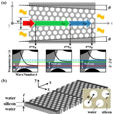
The proposed tapered PC WG design is formed by two PC regions, tilted up and down with angle θ [Fig.1(a)].
The PC regions are two-dimensional (2D) hexagonal lat-tice consisting of holes with radius r ¼ 0:4a, where a is the lattice constant. The entire structure is a free-standing silicon slab of thickness t ¼ 0:59a that is fully immersed in water [Fig. 1(b)]. The refractive indices of silicon and water are set to be 3.46 and 1.33, respectively. Local band diagrams at z ¼ zR, zG, and zBare also shown
in Fig. 1(a). As the WG width gradually becomes nar-rower, the dispersion curve shifts upward accordingly. Waves with λ ¼ λR, λG, and λB propagating along the WG can be decelerated and then reflected by local mode-gap effect (MGE) at z ¼ zR, zG, and zB[11], where
each λ corresponds to the local band edge of the WG
Fig. 1. (Color online) (a) Schematic illustration of the pro-posed tapered PC WG and the corresponding local band diagrams. (b) Illustration of the PC slab structure.
424 OPTICS LETTERS / Vol. 36, No. 3 / February 1, 2011
mode. These positions are defined as the end positions (EPs) of wave propagation and are dependent onλ.
We perform 2D finite-difference time-domain (FDTD) simulations with effective index approximation to calcu-late the transport ability of the tapered PC WG. A TE-polarized cw is launched from the left into the WG of θ ¼ 0:1°. The field distributions with λ varied from 3:20a to 3:00a in steps of 0:05a are shown in Figs. 2(a)–2(e), respectively. When local MGE occurs, the decelerated in-cident and reflected waves form localized standing wave resonance (SWR) at EP, where the field is enhanced lo-cally (indicated by the arrows in Fig.2) [12]. The optical forces produced at EP may trap dielectric particles of size down to a small fraction of wavelength. We can thus use different λ to trap particles at different EPs, which provides advanced controllability on trapping position. In contrast, conventional trapping configurations simply trap particles at a fixed position decided by the structure design. It is worth noting that EP (trapping position) de-pends on λ linearly, and mode profile of the localized SWR does not deform whenλ is varied. These character-istics are advantageous for operation. We can thus trans-port the trapped particles forward or backward along the WG to selected positions by blue-tuning or red-tuningλ gradually, and more importantly, this transport is rever-sible. This feature is unattainable for conventional WG structures, in which the transport can only occur along the propagating direction of wave and is not reversible. Moreover, the tapered PC WG can also stop and hold a particle at different positions along the waveguide. All of these functions can be achieved by simply controllingλ on demand, which greatly enhances the controllability of near-field optical manipulation. To quantify the transport ability, we define a factor S as the distance that the trapped particle moves divided by absolute λ variation. Forθ ¼ 0:1°, S as high as 148 is obtained, which means that the particle can travel148 nm for λ variation of 1 nm. Forθ ¼ 0:5°, the factor S becomes 40.5. For comparison, we simulate a channel WG with tapered design of θ ¼ 0:1°. However, no EP is observed. This confirms that local MGE and localized SWR enhancement only occur in
the tapered PC WG structure, which exclusively per-forms the functions of all-optical controllable trapping and transport of particles on the same platform.
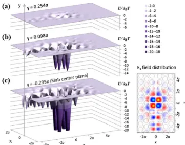
To verify that the tapered PC WG has the ability to trap particles, we calculate the trapping potential U derived from the optical forces on a particle dispersed in water. The particle is assumed to be a polystyrene sphere with refractive index of 1.55, which can mimic most biological molecules. The particle radius is0:098a. For a ¼ 500 nm, the radius about50 nm is the average size of biological viruses. The index contrast is low for the polystyrene par-ticle immersed in water, and the parpar-ticle radius is far smaller than λ=20 when λ is about 3:00a. We can thus use dipole approximation to calculate the optical forces by the equations derived in [13,14]. Moreover, the SWR character balances the scattering force, which makes it negligible compared to the gradient force [6,7]. The par-ticle can thus be trapped at EP by strong gradient force but not disturbed by scattering force. Finally, we can cal-culate the trapping potential experienced by the particle from gradient force solely once the field distribution is known. Here we launch a wave withλ ¼ 3:20a into a ta-pered PC WG with θ ¼ 0:5° by three-dimensional (3D) FDTD simulation to obtain the field distribution. When the input power is7 mW and the slab surface is set to be y ¼ 0, the potential distributions experienced by the par-ticle at different altitudes are shown in Figs.3(a)–3(c). A criterion widely used for stable trapping is to satisfy the requirement that potential depth jUj≧10kBT [1]. Thus,
the trapping gradient force can overcome Brownian mo-tion caused by random thermal perturbamo-tion. When the particle is attracted to the EP on the WG (mass center of the particle is0:098a above the slab surface), the lo-calized SWR leads to four potential wells near EP with depth jUj larger than 10kBT [Fig. 3(b)], where T ¼
300 K (room temperature). The resonant mode profile of localized SWR is shown as the inset of Fig.3. The max-imum depth of12:8kBT is at least eight times deeper than the remaining potential distributed along the WG, which
Fig. 2. (Color online) (a)–(e) Hy-field distributions in the tapered PC WG withθ ¼ 0:1° under different λ as indicated. Localized SWRs at EPs and hence the trapping positions are indicated by the arrows.
Fig. 3. (Color online) Potential distributions near the EP of the tapered PC WG withθ ¼ 0:5° in xz-plane: (a) 0:254a, (b) 0:098a above the slab surface, and (c) at the slab center. The input wavelength λ is 3:20a and the input power is 7 mW. Inset is the Ex-field distribution in xz-plane 0:098a above the slab surface.
demonstrates that stable trapping occurs only near the EP. When we slightly lift the particle up, to0:254a above the slab surface, the potential distribution becomes flat-tened and no trapping well deeper than2kBT can be ob-served [Fig. 3(a)]. This is because the gradient force utilized for trapping results from the evanescent field, in a near-field configuration. In addition, depths and ex-tents of the trapping wells can be adjusted to improve the controllability by varying the launched power or switch-ing the polarization states. The threshold input power of 7 mW for trapping a 50 nm particle stably is quite low compared to the powers required for other waveguide configurations [8–10], which indicates that our design is well suited for practical applications.
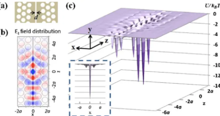
Actually, trapping particles on this WG is accompanied by uncertainty about the trapping position, because the trapping potential is not a single well. Also, particles might be drawn into one of the holes near the trapping wells, which would obstruct the transport. This is be-cause the field is stronger at the slab center. The depths of potential wells distributed at the center plane are dee-per than those above the slab surface [Fig.3(c)]. To deal with these issues, we introduce a slot (width d is 0:2a) at the middle of the WG withθ ¼ 0:5° [Fig.4(a)]. When the input power is1:3 mW and λ is 3:20a, the resonant mode profile and the potential distribution at the slab center near the EP are as shown in Figs.4(b)and4(c), respec-tively. The slot makes the field discontinuity larger at boundaries with high index contrast. In addition to the advantage of small slot width, the field distributes mostly in the slot region [15], which improves the trapping abil-ity. The required input power for reaching a maximum potential depth of 12:6kBT reduces to 1:3 mW, which is much lower than that without a slot. Thus, particles with radius smaller than0:098a can be trapped and trans-ported inside the slot at a low power level. Also, the slot
unifies the lateral double trapping wells into a single well, which eliminates the lateral uncertainty and improves the trapping precision.
In summary, we have proposed that a simple tapered PC WG can trap subwavelength particles at a specified EP depending onλ, and can transport it forward or back-ward to other selected positions by varyingλ gradually. These features are unattainable for conventional trap-ping or transport configurations. Numerical simulations show that on the tapered PC WG withθ ¼ 0:1°, a trapped particle can travel148 nm for only 1 nm λ variation. We also calculate the trapping potential to verify the trapping ability. On the tapered PC WG withθ ¼ 0:5°, a low input power of7 mW can result in strong localized SWR at the EP, which can stably trap the polystyrene particle of 50 nm in radius. A slot structure at the middle of the tapered PC WG can further improve the trapping preci-sion and reduces the required input power. Only1:3 mW is needed to achieve a maximum potential depth of 12:6kBT. We anticipate that this all-optical controllable
trapping and transport of subwavelength particles will be beneficial for future life science research.
This work was supported by Taiwan’s National Science Council (NSC) under contracts NSC-98-2221-E-009-015-MY2 and NSC-99-2120-M-009-009.
References
1. A. Ashkin, J. M. Dziedzic, J. E. Bjorkholm, and S. Chu, Opt. Lett.11, 288 (1986).
2. M. Gu, J. B. Haumonte, Y. Micheau, J. W. M. Chon, and X. Gan, Appl. Phys. Lett.84, 4236 (2004).
3. S. Kawata and T. Sugiura, Opt. Lett.17, 772 (1992). 4. L. Novotny, R. X. Bian, and X. S. Xie, Phys. Rev. Lett.79,
645 (1997).
5. K. Okamoto and S. Kawata, Phys. Rev. Lett.83, 4534 (1999). 6. A. Rahmani and P. C. Chaumet, Opt. Express 14, 6353
(2006).
7. M. Barth and O. Benson, Appl. Phys. Lett. 89, 253114 (2006).
8. S. Kawata and T. Tani, Opt. Lett.21, 1768 (1996). 9. S. Gaugiran, S. Gétin, J. M. Fedeli, G. Colas, A. Fuchs,
F. Chatelain, and J. Dérouard, Opt. Express13, 6956 (2005). 10. A. H. J. Yang, S. D. Moore, B. S. Schmidt, M. Klug, M. Lipson,
and D. Erickson, Nature457, 71 (2009).
11. B. S. Song, S. Noda, T. Asano, and Y. Akahane, Nat. Mater. 4, 207 (2005).
12. T. Baba, D. Mori, K. Inoshita, and Y. Kuroki, IEEE J. Sel. Top. Quantum Electron.10, 484 (2004).
13. Y. Harada and T. Asakura, Opt. Commun.124, 529 (1996). 14. A. Rohrbach and E. H. K. Stelzer, J. Opt. Soc. Am. A18,
839 (2001).
15. V. R. Almeida, Q. Xu, C. A. Barrios, and M. Lipson, Opt. Lett. 29, 1209 (2004).
Fig. 4. (Color online) (a) Schematic illustration of the slotted tapered PC WG. (b) Ez-field distribution at the slab center. (c) The corresponding potential distribution near the EP. 426 OPTICS LETTERS / Vol. 36, No. 3 / February 1, 2011