Free-standing a-plane GaN substrates grown by HVPE
Yin-Hao Wu*, Yen-Hsien Yeh, Kuei-Ming Chen, Yu-Jen Yang, and Wei-I Lee
Department of Electrophysics, National Chiao Tung University, Hsinchu City 30010, Taiwan
ABSTRACT
A-plane free-standing GaN was grown on a-plane GaN templates by HVPE. A-plane GaN templates were grown on r-plane sapphire by MOCVD with multilayer high-low-high temperature AlN buffer layers. A regrowth method was used for growing GaN through HVPE. First, GaN was grown on a-plane GaN templates, followed by separating the a-plane GaN film from r-plane sapphire using LLO. Then, the GaN films were regrown using HVPE. The resulting free-standing GaN contained some voids, which causes to release the stress.
Keywords: Hydride vapor phase epitaxy, non-polar Gallium Nitride, Semiconducting III-V materials,
1. INTRODUCTION
Recently, nitride-based optoelectronic devices have attracted attention. Because of wide band gap, nitride-based material can be applied in visible or ultraviolet light-emitting diodes (LEDs)[1][2] and laser diodes (LDs)[3]. Conventionally, the quantum well (QW) of LED or LD structures is grown on c-plane (0001) sapphire. InGaN/GaN or AlGaN/GaN structure is usually used in QWs. Because c-plane GaN is polar face, QWs are grown on c-plane GaN that exhibits strong electrostatic fields. The fields cause spatial separation of electrons and holes in the QWs[4]. The separation causes the recombination ratio of carrier and influences the efficiency of optoelectronic devices[5]. This phenomenon is called the quantum-confined stark effect (QCSE). The QCSE effect could be improved by growing QWs on semi-polar or non-polar GaN. This has stimulated much research on a-plane GaN.
Because lattice constant of r-plane sapphire is similar to a-plane GaN, a-plane GaN is usually grown on r-plane sapphire. Lattice mismatch causes dislocations or basal stacking faults (BSFs) for a-plane GaN grown on r-plane sapphire. These dislocations increase the leakage current, thereby decreasing device performance. There are many techniques to reduce dislocations or BSFs, such as flow-rate modulation epitaxy, lateral epitaxial overgrowth (LEO)[6][7], and sidewall lateral epitaxial overgrowth (SLEO)[8]. The difference in thermal expansion coefficients of GaN and sapphire leads to a-plane
MOCVD-GaN HT-LT-HT AIN
r-sa pph ire
Growth GaN thick film H VP [-Ga N M OCVD-Ga N HT-LT-HT AIN r-sapph ire separation H VP E-Ga N MOCVD-GaN HT-LT-HT AN r-sapph ire r-sa pph ire
Growth GaN template
GaN film crack during cool-down from growth temperature to room temperature. The epitaxial layers of GaN-based devices have the same thermal expansion coefficient with free-standing GaN substrates. Therefore, GaN-based devices grown on free-standing GaN substrates can diminish cracking. In addition to lattice constant of GaN matching with the epitaxial layer of GaN-based devices, it can also reduce the dislocation density. Growing nitride-based devices on GaN substrate can outperform sapphire[2]. Based on our research of using multilayer high-low-high temperature AlN buffer layers for growing a-plane GaN on r-plane sapphire by metalorganic chemical vapor deposition (MOCVD)[9], we used a-plane GaN film for the non-polar GaN template. We grew a-plane free-standing GaN using hydride vapor phase epitaxy (HVPE) on a-plane GaN templates.
2. EXPERIMENT
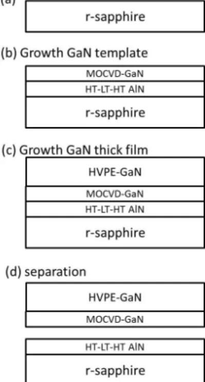
Fig.1 shows the process of growth free-standing a-plane GaN. The a-plane GaN templates were growth using MOCVD on r-plane sapphires. The a-plane GaN templates consists of three AlN buffer layers, which are a high-temperature AlN bottom layer, a low-temperature AlN middle layer, a high-temperature AlN top layer. The high temperature AlN buffer layer was grown at 800℃, and the low temperature AlN buffer layer was grown at 1000℃. The trimethylgallium (TMGa), trimethylaluminum (TMAl), and ammonia (NH3) were used as precursors and hydride was carrier gas. The
2μm a-plane GaN films were grown by MOCVD on the AlN buffer layer as a-plane GaN templates.
Figure 1 Process of producing a-plane free-standing GaN. (a) R-plane sapphire. (b) HT-LT-HT AlN buffer layer and 2μm GaN grown on r-plane sapphire using MOCVD. (c) First a-plane GaN grown on template using HVPE. (d) First a-plane GaN separated from r-plane sapphire using LLO.
Proc. of SPIE Vol. 8262 82621Z-2
The a-plane GaN thick films were grown on a-plane GaN templates using HVPE. GaN were formed by mixing GaCl and NH3 in HVPE system. The a-plane GaN thick films were used the two step growth methods. The first step, the growth
temperature was at 1000℃, and the growth pressure at 100 torr. The growth time was 40 minutes. The second step, the growth temperature was at 1100℃, and the growth pressure at 100 torr. The growth time increased to 120 minutes. After growth a-plane GaN thick films, we used the laser lift off technique to separate the GaN film and sapphire. The laser is used the 355nm Nd:YAG laser. After laser lift off, the separated a-plane GaN films were call as “free-standing a-plane GaN”.
3. RESULTS AND DISCUSSION
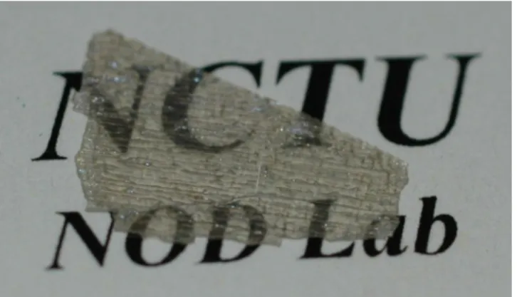
Fig.2 presents the optical image of free-standing a-plane GaN. From the image, we can observe the free-standing GaN is not transparent crystal. The result is attributed to the surface is not much smooth. The surface morphology is shown in Fig.3 by SEM images.
Figure 2 The optical image of free-standing GaN.
Fig.3 shows the SEM images of free-standing a-plane GaN. In the Fig.3(a), the SEM plane view of a-plane GaN, which shows the stripes are along m-direction. The SEM tile and cross-sectional view are shown in Fig.3(b), which shows the stripes are along m-direction more obviously. The growth rates in different orientation are +c-(Ga face), a-, m- and –c-(N-face) in consequence for GaN. The N-face is a cliff, and the Ga-face is a gentle slope. Owing to the high growth rate in HVPE system, the coalescence in m-direction is more obviously than growth using MOCVD system. In the free-standing GaN surface, we can also observe the V-shape pits on the surface.
method. Usin SEM cross-se produce the evaporation. ng the ELOG ectional view, morphology Figure 3 (a) growth meth , which shows which is sim plane view (b
hod can leave s the void in t milar to the E b) tile view an the voids to the a-plane G ELOG. And nd (c) cross-se reduce the str aN film. Thus we can redu ectional free-st rain in the Ga s, using the tw uce the proce
tanding GaN aN films. In F wo step growt ess such as l SEM images Fig3.(c) is the th method can ithography or e n r From the SEM images, the cross-sectional morphology of free-standing a-plane GaN resembles the ELOG growth
Proc. of SPIE Vol. 8262 82621Z-4
The Raman spectrum was used to observe the stress of a-plane GaN. The stress free GaN is 567nm-1 in Raman spectrum. We compared a-plane GaN before and after laser lift off. Before laser lift off, because the lattice constant and thermal expansion coefficient are different with GaN and sapphire, the E2 high mode peak of Raman spectrum of a-plane GaN is 567.53 nm-1. Thus, which is compressive strain. After laser lift off, the strain of free-standing a-plane GaN is relaxed, and the E2 high mode peak of Raman spectrum is 566.61 nm-1. The free-standing a-plane GaN is tensile strain. In the future work, we can homoepitaxial grow GaN on the free-standing GaN to reduce the stress.
4. SUMMARY
The a-plane GaN was grown on a-plane GaN templates using HVPE. We use the HT-LT-HT AlN buffer layer to grow the a-plane GaN templates by MOCVD. The free-stand a-plane GaN was obtained by laser lift off technique. From the SEM images, the a-plane GaN surface is similar to the surface using the ELOG growth method. And we could find voids in the a-plane GaN films, which can release the stress.
REFERENCES
[1] T. Nishida, H. Saito, N. Kobayashi, “Efficient and high-power AlGaN-based ultraviolet light-emitting diode grown on bulk GaN,” Appl. Phys. Lett. 79, 711-713 (2001)
[2] X.A. Cao, S.F. LeBoeuf, M.P. D’Evelyn, S.D. Arthur, J. Kretchmer, C.H. Yan, Z.H. Yang, “Blue and near-ultraviolet light-emitting diodes on free-standing GaN substrates,” Appl. Phys. Lett. 84, 4313-4315 (2004)
[3] S. Nakamura, “InGaN/GaN/AlGaN-based laser diodes grown on free-standing GaN substrates,” Mater. Sci. Eng. B
59, 370-375 (1999)
[4] T. Takeuchi, C. Wetzel, S. Yamaguchi, H. Sakai, H. Amano, I. Akasaki, Y. Kaneko, S. Nakagawa, Y. Yamaoka, N. Yamada,” Determination of piezoelectric fields in strained GaInN quantum wells using the quantum-confined Stark effect,” Appl. Phys. Lett. 73, 1691-1693 (1998)
[5] P. Waltereit, O. Brandt, a Trampert, H. Grahn, J. Menniger, M. Ramsteiner, M. Reiche, K. Ploog,” Nitride semiconductors free of electrostatic fields for efficient white light-emitting diodes,” Nature 406, 865-867 (2000)
[6] M.D. Craven, S.H. Lim, F. Wu, J.S. Speck, S.P. Denbaars,” Nonpolar a-Plane (11-20) Gallium Nitride Thin Films Grown (1-102) r-Plane Sapphire Heteroepitaxy and Lateral Overgrowth,” phys. stat. sol. (a) 194, 541–544 (2002) [7] M.D. Craven, S.H. Lim, F. Wu, J.S. Speck, S.P. DenBaars,” Threading dislocation reduction via laterally overgrown nonpolar (11-20) a-plane GaN,” Appl. Phys. Lett. 81, 1201-1203 (2002)
[8] B. Imer, F. Wu, J. Speck, S. Denbaars,” Growth evolution in sidewall lateral epitaxial overgrowth (SLEO),” J. Cryst. Growth 306, 330-338 (2007)
[9] C.H. Chiang, K.M. Chen, Y.H. Wu, Y.S. Yeh, W.I. Lee, J.F. Chen, K.L. Lin, Y.L. Hsiao, W.C. Huang, E.Y. Chang,” Nonpolar a-plane GaN grown on r-plane sapphire using multilayer AlN buffer by metalorganic chemical vapor deposition,” Appl. Surf. Sci. 257, 2415-2418 (2011)