414 IEEE PHOTONICS TECHNOLOGY LETTERS, VOL. 21, NO. 7, APRIL 1, 2009
Improvement of the Efficiency of InGaN–GaN
Quantum-Well Light-Emitting Diodes Grown With a
Pulsed-Trimethylindium Flow Process
Tao-Hung Hsueh, Jinn-Kong Sheu, Wei-Chi Lai, Yi-Ting Wang, Hao-Chung Kuo, Senior Member, IEEE, and
Shing-Chung Wang, Life Member, IEEE
Abstract—This study demonstrated the enhancement of the
light output power of InGaN–GaN multiple quantum-well light-emitting diodes (LEDs) that are grown with a pulsed-trimethylindium (pulsed-TMIn) flow process by metal–organic vapor-phase epitaxy. At an injection current of 20 mA, the output power of the pulsed-TMIn treated LEDs was improved by 16% as compared to that of the conventional LEDs. In addition, a minor droop (versus injection current) in terms of external quantum efficiency was also observed in the pulsed-TMIn treated LEDs as compared to conventional LEDs. This improvement could be at-tributed to the fact that the significant carrier localization effect in the pulsed-TMIn treated LEDs can lead to higher recombination efficiency. This contention is perhaps tentatively evidenced by the temperature-dependent photoluminescence results in which the activation energy of the pulsed-TMIn treated LEDs was increased by 21.8% as compared to that of conventional LEDs.
Index Terms—External quantum efficiency (EQE), GaN
light-emitting diode (LED), multiple quantum-well (MQW), pulsed-trimethylindium (pulsed-TMIn).
I. INTRODUCTION
T
HE In Ga N–GaN multiple quantum-wells (MQWs) are widely used as the active layer in light-emitting diodes (LEDs) and laser diodes that emit light in the ultravi-olet-blue-green range [1], [2]. According to previous research, the spatial indium concentration fluctuation or exciton local-ization effect tends to dominate the luminescence behavior of the InGaN–GaN MQWs with higher indium concentrations in thin quantum-wells, while the quantum-confined Stark effect (QCSE) dominates the recombination emission in wide quantum-wells [3]. Moreover, research has suggested that carriers in the In Ga N–GaN MQWs that are localized on the local minimum in the energy landscape with a depth that is at least comparable to the thermal energy of the carriers at room temperature could act as a localization site [4], [5]. In general,Manuscript received December 10, 2008; revised December 29, 2008. First published February 03, 2009; current version published March 13, 2009. This work was supported by Frontier Materials and Micro/Nano Science and Tech-nology Center, NCKU, and by the National Science Council under Research Grant NSC 97-2221-E-006-242-MY3.
T.-H. Hsueh, J.-K. Sheu, and W.-C. Lai are with the Institute of Electro-Op-tical Science and Engineering, Center for Micro/Nano Science and Technology, Advanced Optoelectronic Technology Center, National Cheng Kung University, Tainan 701, Taiwan (e-mail: [email protected]; [email protected]. edu.tw; [email protected]).
Y.-T. Wang, H.-C. Kuo, and S.-C. Wang are with the Department of Photonics and Institute of Electro-Optical Engineering, National Chiao Tung University, Hinchu 300, Taiwan (e-mail: [email protected]; [email protected]; [email protected]).
Digital Object Identifier 10.1109/LPT.2009.2012872
the trimethylindium (TMIn) flow rate is unvaried during the growth of InGaN quantum-wells. Some methods, such as the ad-dition of InN interfacial layers between the quantum-wells and the barriers, trapezoid/triangular QWs, and growth interruption between the wells and the barriers, have reportedly improved the internal quantum efficiency of In Ga N–GaN MQW LEDs [6]–[8]. Such methods result in interface improvement and/or the formation of quantum-dot-like clusters for strong localizing carriers [9]. In this letter, we report an approach that improves the light output power of In Ga N–GaN MQW blue LEDs by using a pulsed-TMIn flow process during the growth of the In Ga N QW layers.
II. EXPERIMENTS
All samples used in this study were grown on -plane (0001) sapphire (Al O ) substrates by metal–organic vapor-phase epi-taxy (MOVPE). Trimethyl–gallium (TMGa), TMIn, ammonia, biscyclopentadienil (Cp Mg), and disilane (Si H ) were used as the precursors and dopants. The layer structure consisted of a 30-nm-thick GaN nucleation layer, which was grown at 550 C; a 4- m-thick Si-doped GaN layer, which was grown at 1060 C; an eight-pair In Ga N–GaN MQW active layer, which was grown at 770 C; a 50-nm-thick Mg-doped AlGaN electron blocking layer, which was grown at 1050 C; and a 150-nm-thick Mg-doped GaN cladding layer, which was grown at 1050 C. Each pair of the MQW layers was composed of a 2.5-nm-thick In Ga N well layer and an 11-nm-thick GaN barrier layer. In this work, the was 230 sccm during the growth of each well layer for the conventional LEDs. For the pulsed-TMIn treated LEDs, the , which was provided by two TMIn source lines (i.e., 230 and 170 sccm), was initially 400 sccm and continued for 10% of the growth time for each well layer. After that, the was decreased to 230 sccm by shutting one of the TMIn source lines (i.e., 170 sccm) immediately and maintaining a constant value of 230 sccm with the other TMIn source line until the completion of this well growth. After the growth of the whole LED structure, the LED’s chip process was performed using a standard procedure that is described in detail in a previously published study [10]. Structural characterization was accomplished through high-resolution X-ray diffraction (XRD) using a Bede D1 triple-axis diffractometer with a parabolic graded multilayer Gutman mirror collimator. Photoluminescence (PL) measure-ments using a 325-nm He–Cd laser were utilized to study the optical properties of the LEDs. The light output power was measured using an integrating sphere with a large Si detector (i.e., detector area 10 10 mm ).
HSUEH et al.: IMPROVEMENT OF THE EFFICIENCY OF InGaN–GaN QUANTUM-WELL LEDs 415
Fig. 1. The 10 K normalized PL spectra and XRD spectra (inset) of (0004) reflection for conventional and pulsed-TMIn InGaN–GaN MQW LEDs.
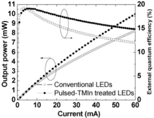
Fig. 2. Output power and EQE versus injection current for conventional and pulsed-TMIn InGaN–GaN MQW LEDs.
III. RESULTS ANDDISCUSSION
The PL spectra of the conventional and pulsed-TMIn treated LEDs are shown in Fig. 1. The conventional LEDs emit at a peak energy of around 2.79 eV and a full-width at half-maximum (FWHM) of 80 meV, while the pulsed-TMIn treated LEDs emit at a peak energy of around 2.81 eV and an FWHM of 53 meV. Notably, the FWHM of the pulsed-TMIn treated LEDs is 34% narrower in terms of magnitude than that of the conventional LEDs. In addition, the pulsed-TMIn treated LEDs show a blueshift of approximately 20 meV relative to that of conventional LEDs, as shown in Fig. 1. The inset of Fig. 1 shows the (0004) reflection XRD spectra for both sam-ples, which exhibit apparent satellite peaks within the scanning range. This implies that the interfaces between the wells and the barriers of both LEDs are sufficiently sharp. By combining the measured XRD spectra and the simulation results in addition to following the method of dynamical theory [11], both LEDs are found to be similar in terms of MQW structures, including the nearly consistent well and barrier thickness and average indium content. The thickness of the GaN barrier and the In Ga N well layers were around 11.2 and 2.45 nm, respectively. The indium content of the InGaN QWs was around 22% for both LEDs.
The light output power and external quantum efficiency (EQE) are shown as a function of injection current for both LEDs in Fig. 2. At a low injection current level (i.e., 10 mA), the output power of the pulsed-TMIn LEDs was similar to that of the conventional LEDs, whereas at a higher injection current level (i.e., 10 mA), the output power of the pulsed-TMIn LEDs is markedly higher than that of the conventional LEDs.
At an injection current of 20 mA, the output power values of the conventional and pulsed-TMIn treated LEDs are 3.1 and 3.6 mW, respectively. Clearly, the 20-mA output power of the pulsed-TMIn LEDs is improved by approximately 16% as compared to that of the conventional LEDs. In addition, the graph of the light output power versus the injection current shows similar and typical characteristics for both LEDs, which can be seen in Fig. 2. However, the graph of the EQE versus the injection current shows a fundamentally different behavior. The EQE sharply increases at low injection currents (i.e., 5 mA) and then starts to droop as the current increases for both LEDs, which is universally observed in high-quality InGaN–GaN MQW LEDs [12]. In addition to the presence of an efficiency droop at high injection currents, the conventional LEDs show a faster droop in terms of EQE as compared to the pulsed-TMIn LEDs. For example, the EQE values at an injection current of 60 mA are approximately reduced by 19.7% and 30.4% for the pulsed-TMIn treated and conventional LEDs, respectively, as compared to the EQE at an injection current of 20 mA.
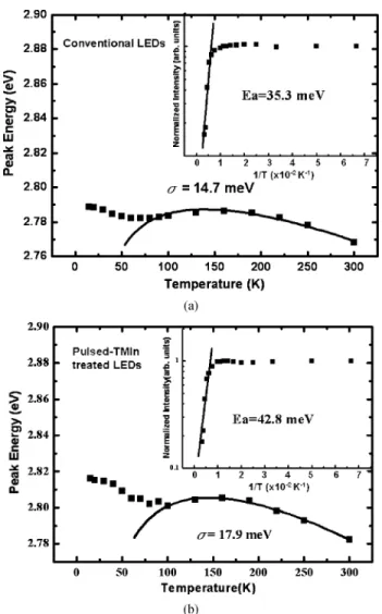
To clarify the reason for the enhancement of output power and the minor EQE droop effect in the InGaN–GaN MQW LEDs that were grown with a pulsed-TMIn process, temperature-dependent PL measurements were performed and examined using the Varshni law [13]. Fig. 3 shows the PL peak energy as a function of temperature. Obviously, both curves do not follow the Varshni law and show an “S” shape (i.e., redshift–blueshift–redshift) over a temperature range from 10 K to 300 K, indicating the existence of localized states in both samples [14]–[16]. The localization effects can be studied by the band tail model as suggested by Eliseev et al., which is as follows: [15]
(1) The first term [i.e., ] describes the energy gap at zero tem-perature; and are known as Varshni’s fitting parameters. The third term comes from the localization effect, in which indicates the degree of localization effect. Additionally, is Boltzmann’s constant. The value of was determined to be 14.7 and 17.9 meV for the conventional and pulsed-TMIn treated LEDs, respectively. In particular, the degree of localization ef-fects in the pulsed-TMIn LEDs is 21.8% higher in terms of than that of the conventional LEDs. The insets of Fig. 3 show Arrhenius plots of the normalized integrated PL intensity for the InGaN-related PL emission over the temperature range. For K, thermal quenching can be fitted with activation energies ( ) of 35.3 and 42.8 meV for the conventional and pulsed-TMIn LEDs, respectively, implying an improvement of 21.2% in terms of . Previous research has suggested that the in InGaN–GaN MQWs represents the localization energies of excitons resulting from band edge fluctuations [16].
Generally, the thermal quenching of PL intensity with tem-perature can be explained by the thermal emission of the carriers out of a confining potential with an activation energy that is cor-related with the depth of the confining potential [14]. Studies have suggested that the localization of carriers operates as ex-cellent radiative recombination centers. In other words, high lo-calization energies of excitons will cause a minor overflow of carriers outside the InGaN MQW active region [1]. This kind of InGaN QW will not have a smooth, sloping band edge, which
416 IEEE PHOTONICS TECHNOLOGY LETTERS, VOL. 21, NO. 7, APRIL 1, 2009
Fig. 3. PL peak energies versus temperature for (a) conventional and (b) pulsed-TMIn treated InGaN–GaN MQW LEDs. The solid lines are fitting results obtained using (1). The insets show the normalized PL intensity as a function of1=T for conventional and pulsed-TMIn InGaN–GaN MQW LEDs.
could reduce or even eliminate the influence of QCSE on op-tical properties. Scholars have suggested that the confinement provided by the regions previously mentioned can overcome the negative effect of the polarization field in MQW active region [17]. Moreover, the polarization field in the MQW active re-gion is suggested to be the origin of the efficiency droop that occurs in InGaN–GaN MQW LEDs. In other words, the effi-ciency droop is caused by a carrier recombination outside the MQW active region with considerable polarization fields [12]. Therefore, we attribute the improvement in output power and the reduction in efficiency droop of the pulsed-TMIn treated LEDs to better localization effects or improved carrier confinement in the InGaN–GaN MQW active region, which is induced by the pulsed-TMIn process during the growth of InGaN QWs.
IV. SUMMARY
In this letter, we have demonstrated a pulsed-TMIn flow process during the growth of InGaN QWs, which leads to an improvement of light output power in InGaN–GaN MQW blue LEDs. The reduction of efficiency droop at a high injection current level was also observed in the pulsed-TMIn LEDs.
The temperature-dependent measurements have shown that the significant localization effect for the pulsed-TMIn LEDs as compared to the conventional LEDs can improve the ra-diative recombination rate (i.e., internal quantum efficiency) of InGaN–GaN MQW LEDs. Based on the aforesaid results, the pulsed-TMIn technique is a controllable and realizable technique for the growth of InGaN–GaN MQW LEDs by MOVPE and is applicable to the fabrication of high efficiency, nitride-based LEDs for solid-state lighting.
REFERENCES
[1] S. Nakamura and S. F. Chichibu, Introduction to Nitride Semiconductor Blue Lasers and Light Emitting Diodes. New York: Taylor & Francis, 2000.
[2] Y. Narukawa, Y. Kawakami, M. Funato, S. Fujita, and S. Nakamura, “Role of self-formed InGaN quantum dots for exciton localization in the purple laser diode emitting at 420 nm,” Appl. Phys. Lett., vol. 70, pp. 981–983, 1997.
[3] N. A. Shapiro, P. Perlin, C. Kisielowski, L. S. Mattos, J. W. Yang, and E. R. Weber, “The effects of indium concentration and well-thickness on the mechanisms of radiative recombination in In Ga N quantum wells,” MRS Internet J. Nitride Semicond. Res., vol. 5, p. S1, 2000. [4] K. Watanabe, J. R. Yang, N. Nakanishi, K. Inoke, and M. Shiojiri,
“Direct determination of atomic structure in multiple quantum wells InGaN/GaN,” Appl. Phys. Lett., vol. 80, pp. 761–763, 2002. [5] H. K. Cho, J. Y. Lee, N. Sharma, C. J. Humphreys, G. M. Yang, and
C. S. Kim, “Effect of growth interruptions on the light emission and indium clustering of InGaN/GaN multiple quantum wells,” Appl. Phys. Lett., vol. 79, pp. 2594–2596, 2001.
[6] Y. C. Cheng, C. M. Wu, M. K. Chen, C. C. Yang, Z. C. Feng, G. A. Li, J. R. Yang, A. Rosenauer, and K. J. Ma, “Improvements of InGaN/GaN quantum-well interfaces and radiative efficiency with InN interfacial layers,” Appl. Phys. Lett., vol. 84, pp. 5422–5424, 2004.
[7] M. G. Cheong, C. Liu, H. W. Choi, B. K. Lee, E. K. Suh, and H. J. Lee, “Study of the origin of luminescence in high indium composition InGaN/GaN quantum wells,” J. Appl. Phys., vol. 93, pp. 4691–4695, 2003.
[8] J. P. Liu, R. Q. Jin, J. J. Zhu, J. C. Zhang, J. F. Wang, M. Wu, J. Chen, Y. T. Wang, and H. Yang, “Effects of TMIn flow on the interface and optical properties of InGaN/GaN mutiple quantum wells,” J. Cryst. Growth, vol. 264, pp. 53–57, 2004.
[9] S. Nskamura, M. Senoh, S. Nagahama, N. Iwasa, T. Yamada, T. Matsushita, Y. Sugaimoto, and H. Kikyokau, “Subband emissions of InGaN multi-quantum-well laser diodes under room-temperature continuous wave operation,” Appl. Phus. Lett., vol. 70, pp. 2753–2755, 1997.
[10] J. K. Sheu, C. H. Kuo, S. J. Chang, Y. K. Su, L. W. Wu, Y. C. Lin, W. C. Lai, J. M. Tsai, G. C. Chi, and R. K. Wu, “White-light emission from near UV InGaN–GaN LED chip precoated with blue/green/red phosphors,” IEEE Photon. Technol. Lett., vol. 15, no. 1, pp. 18–20, Jan. 2003.
[11] I. H. Kim, H. S. Park, Y. I. Park, and T. Kim, “Formation of V-shaped pits in InGaN/GaN multiquantum wells and bulk InGaN films,” Appl. Phys. Lett., vol. 73, pp. 1634–1636, 1998.
[12] Y.-C. Shen, G. O. Mueller, S. Watanabe, N. F. Gardner, A. Munkholm, and M. R. Krames, “Auger recombination in InGaN measured by pho-toluminescence,” Appl. Phys. Lett., vol. 91, pp. 141101–141103, 2007. [13] Y. P. Varshni, “Temperature dependence of the energy gap in
semicon-ductors,” Physica, vol. 34, pp. 149–154, 1967.
[14] Y. H. Cho, G. H. Gainer, A. J. Fischer, J. J. Song, S. Keller, U. K. Mishra, and S. P. DenBaars, ““S-shaped” temperature-dependent emission shift and carrier dynamics in InGaN/GaN multiple quantum wells,” Appl. Phys. Lett., vol. 73, pp. 1370–1372, 1998.
[15] P. G. Elixeev, P. Perlin, J. Lee, and M. Osinski, ““Blue” temperature-induced shift and band-tail emission in InGaN-based light sources,” Appl. Phys. Lett., vol. 71, pp. 569–571, 1997.
[16] M. Smith, G. D. Chen, J. Y. Lin, H. X. Jiang, M. Asif Khan, and Q. Chen, “Time-resolved photoluminescence studies of InGaN epilayers,” Appl. Phys. Lett., vol. 69, pp. 2837–2839, 1996.
[17] M. B. Nardelli, K. Rapcewicz, and J. Bernholc, “Polarization field effects on the electron-hole recombination dynamics in In Ga N/In Ga N multiple quantum wells,” Appl. Phys. Lett., vol. 71, pp. 3135–3137, 1997.