High Electron Mobility AlGaN/AlN/GaN HEMT Structure With a
Nano-scale AlN Interlayer
Shih-Chun Huang
a, Wen-Ray Chen*
a, Yu-Ting Hsu
b, Jia-Ching Lin
c, Kuo-Jen Chang
c, and Wen-Jen
Lin
ca
Graduate Institute of Electro-Optical and Materials Science, National Formosa University,
Yunlin 632, Taiwan, R.O.C.
b
Department of Electrophysics, National Chiao Tung University, Hsinchu 300, Taiwan, R.O.C.;
cMaterials and Electro-Optics Research Division, Chung Shan Institute of Science and Technology,
Taoyuan 325, Taiwan, R.O.C.
ABSTRACTEpitaxies of AlGaN/AlN/GaN high electron mobility transistor (HEMT) structures with different thickness of nano-scale AlN interlayers have been realized by metalorganic chemical vapor deposition (MOCVD) technology. After epitaxy, high resolution X-ray diffraction (HRXRD), temperature-dependent Hall Effect and atomic force microscopy (AFM) measurements were used to characterize the properties of these samples. First, it was found that the Al composition of AlGaN layer increases from 21.6 to 34.2% with increasing the thickness of AlN interlayer from 0 to 5 nm under the same AlGaN growth conditions. This result may due to the influences of compressive stress and Al incorporation induced by the AlN interlayer. Then, we also found that the room-temperature (RT) electron mobility stays higher than 1500 cm2/Vs in the samples within AlN interlayer thickness range of 1.5 nm, on the other hand, the low-temperature
(80K) electron mobility drops dramatically from 8180 to 5720 cm2/Vs in the samples with AlN interlayer thickness
increasing from 1 to 1.5 nm. Furthermore, it was found that the two-dimensional electron gas (2DEG) density increases from 1.15×10¹³ to 1.58×1013 cm-2 beyond the AlN interlayer thickness of 1 nm. It was also found that the
temperature-independent 2DEG densities are observed in the samples with AlN interlayer thickness of 0.5 and 1 nm. The degenerated characteristics of the samples with AlN thickness thicker than 1.5 nm show the degraded crystalline quality which matched the observation of surface defects and small cracks formations from their AFM images. Finally, the 2DEG mobilities of the proposed structures can be achieved as high as 1705 and 8180 cm2/Vs at RT and 80K, respectively.
Keywords: GaN, AlN, AlGaN, HEMT, interlayer, 2DEG
1. INTRODUCTION
For the next generation communication technology featuring high speed and high volume, high power electrical devices are necessary. Semiconductors are the promising materials to achieve this application. Especially the spectacular materials, GaN-based semiconductors, are very suitable for manufacturing high frequency and high power devices. Due to their large bandgap, large breakdown voltage, and strong spontaneous and piezoelectric polarization fields, GaN-based power devices also guarantee a satisfying operation in high temperature and caustic environments1. Therefore,
AlGaN/GaN HEMT devices have attracted many attentions in recent years. In this material system, a two-dimensional electron gas formed at the AlGaN/GaN interface will induce a high electron density channel which resulted in high electron mobility and concentration. In addition, for the purpose to increase 2DEG density, one can increase Al mole fraction in the AlGaN barrier layer. However, the growth of high crystalline quality AlGaN barrier layer with high Al composition on GaN is difficult due to the large lattice mismatch between GaN and AlN (aGaN=3.189Å, aAlN=3.112Å).
Otherwise, the poor crystalline quality of AlGaN barrier layer in AlGaN/GaN HEMT structures will also cause a degradation of electrical characteristics in both material and device properties. Thus, based on the idea of creating a high barrier potential in the 2DEG structure, a nano-scale AlN interlayer introduced at the AlGaN/GaN interface has become popular recently2-5. The advantages of introducing this thin AlN interlayer are the better carrier confinement and the
decreased alloy disorder scattering in the 2DEG region, which can enhance the 2DEG mobility and density. Usually the 2DEG mobility can exceed 1500 cm2/Vs and the electron sheet density still can keep at the order of 1013 cm-2 in the
*chenwr@nfu.edu.tw
Nanoepitaxy: Materials and Devices IV, edited by Nobuhiko P. Kobayashi, A. Alec Talin, M. Saif Islam, Proc. of SPIE Vol. 8467, 84670W · © 2012 SPIE · CCC code: 0277-786/12/$18 · doi: 10.1117/12.929347
Proc. of SPIE Vol. 8467 84670W-1
2.50 5.00 2.50 5.00 u m
A1N lnm
2.50 5.00 2.50AIN 2.5nm
5.000pm ó 2.50 5.00 2.50 0A1N Snm
5.00in 0 2.50 5.00 2.50 0 5.00AlGaN/AlN/GaN HEMT structures3-5. In this paper, the effect of AlN interlayer thickness on surface morphologies,
crystalline structures and electrical properties in the AlGaN/AlN/GaN HEMT structures will be discussed in detail.
2. EXPERIMENTS
The AlGaN/AlN/GaN HEMT structures used in this study were all grown on 2 in. c-plane (0 0 0 1) sapphire substrates by a low-pressure vertical-type metalorganic chemical vapor deposition system. Trimethylgallium (TMGa), trimethylaluminum (TMAl) and ammonia (NH3) were employed as gallium, aluminum and nitrogen sources, respectively. Hydrogen (H2) was used as the carrier gas during the epitaxy. Prior to the growth, sapphire substrates were firstly heated to 1130°C in a stream of hydrogen to clean the substrate surfaces. Then a two-step growth procedure was employed with a low-temperature GaN nucleation layer grown at 550°C and the high-temperature epitaxial layers grown at 1030°C. The AlGaN/AlN/GaN HEMT structures consist of a 25-nm-thick GaN nucleation layer, a 2.3-μm-thick undoped GaN layer, a AlN interlayer with different thickness, and a 25-nm-thick AlGaN barrier layer. For comparison, samples without the AlN interlayer were also prepared. All samples have the same growth conditions of GaN and AlGaN epitaxial layers except the growth time of the AlN interlayer. After the growth, atomic force microscopy measurements were carried out to reveal the sample surface morphologies. The epilayer structures and compositions were measured by high resolution X-ray diffraction. Temperature-dependent Hall Effect measurements were used to characterize the electrical properties of these HEMT structures by 1×1 cm2 van der Pauw samples.
3. RESULTS AND DISCUSSIONS
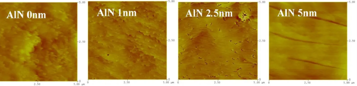
Figure 1 shows the surface morphologies of the samples with AlN interlayer thickness varied from 0 to 5 nm as measured by AFM. In the samples with AlN interlayer thickness larger than 1 nm, the surface cracks appearance can be seen clearly. With increasing the thickness of AlN interlayer, the shapes of the cracks change from small and short to bigger and longer as seen in the AFM images labelled AlN 2.5 and 5 nm. Recently, Smorkchkova et al. had reported that the strain relaxation starts when the thickness of AlN layer exceeds 4 nm in the AlN/GaN heterostructure3. Nevertheless,
in the AlGaN/AlN/GaN heterostructure, the AlN interlayer not only suffers a tensile strain from the below GaN layer but also suffers another tensile strain form the above AlGaN layer. Thus, the strain relaxation should happen within a thinner range of AlN thickness in the AlGaN/AlN/GaN heterostructure and reveal on AlGaN surface by cracks. Moreover, the root-mean-square (RMS) roughness values of the samples with 0, 1, 2.5 and 5 nm AlN interlayer thickness are 0.445, 0.382, 0.603 and 0.684 nm, respectively. Although the cracks and rougher surfaces show that the qualities of AlGaN barrier layers have degraded in the samples with thicker AlN interlayer thickness. Inserting a 1-nm-thick AlN layer at the AlGaN/GaN interface also shows an improved smooth surface morphology as observed from the AFM results.
Figure 1. AFM images showing 5×5 μm2 scans of the samples with varied AlN interlayer thickness. The RMS roughness
values of the samples with 0, 1, 2.5 and 5 nm AlN interlayer thickness are 0.445, 0.382, 0.603 and 0.684 nm, respectively.
Proc. of SPIE Vol. 8467 84670W-2
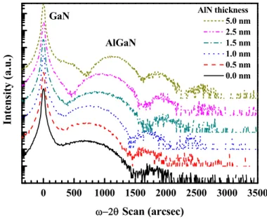
Figure2 shows the high-resolution X-ray diffraction (0002) ω-2θ patterns of the AlGaN/AlN/GaN structures with different AlN interlayer thickness. Two peaks related to GaN and AlGaN epitaxial layers can be seen obviously. It is also found that the AlGaN related peak was separated farther from GaN related peak with increasing the thickness of AlN interlayer. As we mentioned above, however, the growth conditions of AlGaN barrier layers for all samples are the same. Thus, this farther separation phenomenon between GaN and AlGaN peaks must be induced by the AlN interlayer. For further investigation, the Al composition of the AlGaN barrier layer was deduced from the HRXRD measurements results and shown in Figure 3. It is found that an abrupt jump can be observed when the thickness of AlN interlayer exceeds 1 nm. When an AlGaN layer was grown on an AlN layer, this AlGaN layer was under a compressive stress from the below AlN layer, which made the c lattice constant of top AlGaN layer longer than it was. Once the strain was released (crack), the c lattice constant of top AlGaN layer returned to its normal. This behavior would be reflected on HRXRD measurement; in other words, the separation between AlGaN and GaN related peaks became longer as shown in Figure 3. This phenomenon is also well consistent with the investigations of the AFM results. Additionally, it was also reported that the AlN interlayer could induce more Al incorporation in the following AlGaN epitaxial layers6. Therefore,
the higher Al composition in the AlGaN barrier layer should be observed with increasing the thickness of AlN interlayer.
0 500 1000 1500 2000 2500 3000 3500 AlN thickness 5.0 nm 2.5 nm 1.5 nm 1.0 nm 0.5 nm 0.0 nm AlGaN Intensi ty ( a.u.) ω−2θScan (arcsec) GaN
Figure 2. HRXRD (0002) ω-2θscans of the AlGaN/AlN/GaN structures with different AlN interlayer thickness.
0 1 2 3 4 5 20 22 24 26 28 30 32 34 Al com pos it ion of Al G aN laye r ( % )
Thickness of AlN interlayer (nm)
Figure 3. Al composition of AlGaN layer in the AlGaN/AlN/GaN structures as a function of AlN interlayer thickness. The circle shows the abrupt jump with AlN thickness exceeding 1 nm. The soild lines are eye-guiding lines.
Proc. of SPIE Vol. 8467 84670W-3
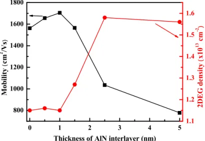
The room-temperature 2DEG mobility and density of our HEMT structures, measured by Hall measurements, were shown in Figure 4. It can be seen that the sample without AlN interlayer has the mobility as high as 1562 cm2/Vs. This
high mobility value shows that the crystalline quality of epitaxial layers in our HEMT structures is good enough to achieve the high performance device request. Furthermore, the highest RT mobility of 1705 cm2/Vs can be realized in
the sample with 1-nm-thickness AlN interlayer. The increment of 2DEG mobility can be attributed to the reduction of AlGaN alloy disorder scattering by inserting a 1-nm-thickness AlN interlayer. On the other hand, the 2DEG density exactly increases at the samples with thicker AlN thickness (> 1 nm) and reaches the highest value of 1.58×1013 cm-2 due
to the suppression of carrier penetration into the AlGaN layer and the enhancement of carrier confinement in the GaN channel. Unfortunately, the mobility also drops rapidly with increasing AlN interlayer thickness over 1 nm. With thicker AlN thickness, the more percentage of carriers penetrated into AlN layer; however, the mobility in AlN is much lower than that of GaN5. This could be the partly reason to the reduction of the mobility. Another possible reason is that the
rougher surface and the cracks, as shown in AFM images, would degrade the carrier transport characteristics of 2DEG channel. In addition, the sample with the highest mobility also has the 2DEG density higher than 1.0×1013 cm-2. Figure 5
shows the sheet resistivity of the HEMT structures as a function of AlN interlayer thickness. Apparently, the one with 1 nm AlN thickness has the lowest sheet resistivity of 245 Ω/sq.
0 1 2 3 4 5 800 1000 1200 1400 1600 1800 1.1 1.2 1.3 1.4 1.5 1.6 Mob ility ( cm 2 /Vs )
Thickness of AlN interlayer (nm)
2DEG density ( x1 0 13 cm -2 )
Figure 4. Room-temperature 2DEG mobility and density of AlGaN/AlN/GaN HEMT structures with different AlN interlayer thickness. 0 1 2 3 4 5 200 250 300 350 400 450 500 550 Sh eet Res istivity ( Ω /sq )
Thickness of AlN interlayer (nm)
Figure 5. Room-temperature sheet resistivity of AlGaN/AlN/GaN HEMT structures as a function AlN interlayer thickness. The solid line is guide for the eye.
Proc. of SPIE Vol. 8467 84670W-4
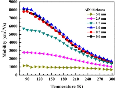
The further investigations of electrical characteristics for the AlGaN/AlN/GaN HEMT structures were measured by temperature-dependent Hall measurements. The temperature-dependent mobility and 2DEG density measured results are shown in Figure 6 and 7, respectively. As seen in Figure 6, similarly to RT mobility, the sample without AlN interlayer has high 80K mobility as 8080 cm2/Vs. And this mobility value can reach as high as 8180 cm2/Vs for the sample with
1-nm-thickness AlN interlayer. All these high mobilities again point out that the crystalline quality of our HEMT structures is superior. Otherwise, the low 80K mobility observed at the samples with thicker (> 1nm) AlN interlayer thickness shows that the interface roughness would become the dominant mobility scattering process, which refers to the AFM results. On the other hand, as seen in Figure 7, the almost identical 2DEG density in the samples with AlN interlayer thickness of 1 nm and below suggests that the conduction is dominated nearly exclusively by the carriers at the AlN/GaN interface. Other samples with and over 1.5 nm AlN interlayer thickness reveal an increasing tendency in 2DEG density with increasing measured temperature. This tendency is similar to temperature-dependent electron density of bulk GaN7,
which means that the characteristics of 2DEG density is degrading with the increment of AlN interlayer thickness. This degradation in 2DEG density is also consistent with the observations of AFM and HRXRD measurements.
90 120 150 180 210 240 270 300 0 1000 2000 3000 4000 5000 6000 7000 8000 9000 Mobili ty ( cm 2 /Vs ) Temperature (K) AlN thickness 5.0 nm 2.5 nm 1.5 nm 1.0 nm 0.5 nm 0.0 nm
Figure 6. Temperature-dependent mobility of AlGaN/AlN/GaN HEMT structures with different AlN interlayer thickness. 90 120 150 180 210 240 270 300 1.0 1.1 1.2 1.3 1.4 1.5 1.6 AlN thickness 5.0 nm 1.0 nm 2.5 nm 0.5 nm 1.5 nm 0.0 nm 2DEG d ens ity ( x1 0 13 cm -2 ) Temperature (K)
Figure 7. Temperature-dependent 2DEG density of AlGaN/AlN/GaN HEMT structures with different AlN interlayer thickness. The sample with 5 nm AlN thickness has an unstable data point which may due to the high sheet resistivity of this sample, as shown in Fighre 5.
Proc. of SPIE Vol. 8467 84670W-5
4. CONCLUSIONS
The AlGaN/AlN/GaN HEMT structures with a nano-scale AlN interlayer have been realized by a vertical-type MOCVD system. It is found that the sample with 1-nm-thickness AlN interlayer has an improved surface morphology. Besides, the cracks can be observed on the surface of the samples with AlN thickness over 1.5 nm, which due to the strain relaxation. This phenomenon also can be found from HRXRD measurement results. Furthermore, we also found that the Al composition of AlGaN layer increases with increasing the thickness of AlN interlayer form the benefit of Al incorporation by AlN interlayer. On the other hand, the highest RT and 80K mobility can be accomplished for the sample with 1-nm-thickness AlN interlayer to the value of 1705 and 8180 cm2/Vs, respectively. This high mobility
sample also has 2DEG density as high as 1.15×1013 cm-2 and independent of temperature.
ACKNOWLEDGMENT
This work was supported by National Science Council of R.O.C. by a Contract no. NSC-100-2221-E-150-064 and Ministry of Economic Affairs of R.O.C. by a Contract no. 101-EC-17-A-04-01-0310.
REFERENCES
[1] Morkoc, H., [Handbook of Nitride Semiconductors and Devices], Wiley-VCH, Berlin, Vols. I-III (2008). [2] Hsu, L. and Walukiewicz, W., "Effect of polarization fields on transport properties in AlGaN/GaN
heterostructures," J. Appl. Phys. 89, 1783-1789 (2001).
[3] Smorchkova, I. P., Chen, L., Heikman, S., Moran, B., Keller, S., DenBaars, S. P., Speck, J. S., and Mishra, U. K., "AlN/GaN and (Al,Ga)N/AlN/GaN two-dimensional electron gas structures grown by plasma-assisted molecular-beam epitaxy," J. Appl. Phys. 90, 5196-5201 (2001).
[4] Miyoshi, M., Egawa, T., and Ishikawa, H., "Study on mobility enchancement in MOVPE-grown AlGaN/AlN/GaN HEMT structures using a thin AlN interfacial layer," Solid-State Electron. 50, 1515-1521 (2006).
[5] Hu, W., Ma, B., Li, D., Miyagawa, R., Miyake, H., and Hiramatsu, K., "Effects of the AlN interlayer on the distribution and mobility of two-dimensional electron gas in AlGaN/AlN/GaN heterojunctions," Jpn. J. Appl.
Phys. 49, 035701 (2010).
[6] Qin, Z. X., Luo, H. J., Chen, Z. Z., Yu, T. J., Yang, Z. J., Xu, K., and Zhang, G. Y., "Effects of the AlN interlayer on incorporation efficiency of Al composition in AlgaN grown by MOVPE," J. Crystal Growth 298, 354-356 (2007).
[7] Lin, J. C., Su, Y. K., Chang, S. J., Chen, W. R., Chen, R. Y., Cheng, Y. C., and Lin, W. J., "Activation energy of n-GaN epitaxial layers grown on vicinal-cut sapphire substrates," J. Crystal Growth 285, 481-485 (2005).
Proc. of SPIE Vol. 8467 84670W-6