Efficiency droop alleviation in InGaN/GaN light-emitting diodes by graded-thickness
multiple quantum wells
C. H. Wang, S. P. Chang, W. T. Chang, J. C. Li, Y. S. Lu, Z. Y. Li, H. C. Yang, H. C. Kuo, T. C. Lu, and S. C. Wang
Citation: Applied Physics Letters 97, 181101 (2010); doi: 10.1063/1.3507891 View online: http://dx.doi.org/10.1063/1.3507891
View Table of Contents: http://scitation.aip.org/content/aip/journal/apl/97/18?ver=pdfcov
Published by the AIP Publishing
Articles you may be interested in
Effect of V-defects on the performance deterioration of InGaN/GaN multiple-quantum-well light-emitting diodes with varying barrier layer thickness
J. Appl. Phys. 114, 143706 (2013); 10.1063/1.4824801
The effect of silicon doping in the barrier on the electroluminescence of InGaN/GaN multiple quantum well light emitting diodes
J. Appl. Phys. 114, 103102 (2013); 10.1063/1.4820450
Improved hole distribution in InGaN/GaN light-emitting diodes with graded thickness quantum barriers
Appl. Phys. Lett. 102, 243504 (2013); 10.1063/1.4811698
Efficiency and droop improvement in green InGaN/GaN light-emitting diodes on GaN nanorods template with SiO2 nanomasks
Appl. Phys. Lett. 101, 233104 (2012); 10.1063/1.4768950
Effect of n-GaN thickness on internal quantum efficiency in InxGa1-xN multiple-quantum-well light emitting diodes grown on Si (111) substrate
J. Appl. Phys. 109, 113537 (2011); 10.1063/1.3596592
This article is copyrighted as indicated in the article. Reuse of AIP content is subject to the terms at: http://scitation.aip.org/termsconditions. Downloaded to IP: 140.113.38.11 On: Wed, 30 Apr 2014 09:56:33
Efficiency droop alleviation in InGaN/GaN light-emitting diodes
by graded-thickness multiple quantum wells
C. H. Wang,1,a兲 S. P. Chang,1,2W. T. Chang,3J. C. Li,1,b兲 Y. S. Lu,1Z. Y. Li,1H. C. Yang,2 H. C. Kuo,1,c兲T. C. Lu,1and S. C. Wang1
1
Department of Photonics and Institute of Electro-Optical Engineering, National Chiao-Tung University, Hsinchu 300, Taiwan
2
R&D Division, Epistar Co. Ltd., Science-based Industrial Park, Hsinchu 300, Taiwan
3
Department of Electro-Physics, National Chiao-Tung University, Hsinchu 300, Taiwan
共Received 15 June 2010; accepted 11 October 2010; published online 1 November 2010兲
InGaN/GaN light-emitting diodes 共LEDs兲 with graded-thickness multiple quantum wells 共GQW兲 was designed and grown by metal-organic chemical vapor deposition. The GQW structure, in which the well-thickness increases along关0001兴 direction, was found to have superior hole distribution as well as radiative recombination distribution by performing simulation modeling. Accordingly, the experimental investigation of electroluminescence spectrum reveals additional emission from the narrower wells within GQWs. Consequently, the efficiency droop can be alleviated to be about 16% from maximum at current density of 30 to 200 A/cm2, which is much smaller than that for conventional LED共32%兲. Moreover, the light output power was enhanced from 18.0 to 24.3 mW at 20 A/cm2. © 2010 American Institute of Physics.关doi:10.1063/1.3507891兴
Solid-state lightings, especially InGaN/GaN light-emitting diodes 共LEDs兲, have been vigorously developed to take the place of traditional lighting source, due to its poten-tially higher efficiency. However, as the efficiency of LEDs increasing, the upcoming challenge is the efficiency “droop” for high-power applications.1It means that the efficiency re-duces rapidly when LED operating under high carrier den-sity. The major cause of efficiency droop is still a huge con-troversy. Various possible mechanisms of droop including carrier overflow,2nonuniform distribution of holes,3,4Auger scattering,5carrier delocalization6have been proposed. In re-cent years, great efforts have been made to reduce the effi-ciency droop. Most of them are focus on minimizing the carrier overflow by reducing or eliminating the polarization field in the active region, such as using polarization-matched multiple quantum wells 共MQWs兲,7,8staggered InGaN quan-tum wells,9and nonpolar or semipolar GaN substrate.10 But for improving hole distribution, only several approaches, such as p-type MQWs11 or coupled quantum wells,12 are explored. However, in the p-type MQWs, the Mg-dopant is very likely to diffuse into wells, while in the coupled quan-tum wells, electrons are tend to overflow by using thin bar-riers. These will result in reduction of radiative efficiency. In this research, we designed and grew a LED structure with graded-thickness multiple quantum wells 共GQWs兲 by using metal-organic chemical vapor deposition 共MOCVD兲. Better hole distribution in such graded-thickness designed MQWs were demonstrated by APSYS simulation as well as the elec-troluminescence 共EL兲 measurements. As a result, the effi-ciency droop behavior was alleviated while the radiative re-combination was improved.
The LED structures were grown on c-plane sapphire substrates by MOCVD. A 20-nm-thick low temperature GaN nucleation layer followed by a 4 m n-type GaN buffer
layer, ten-pair InGaN/GaN superlattice were grown on the top of sapphire. After that, six-pair MQWs were grown with 10-nm-thick GaN barriers. For our designed experiment, the thicknesses of In0.15Ga0.85N quantum wells for GQW LED
structure, controlled by growth time, are 1.5, 1.8, 2.1, 2.4, 2.7, and 3 nm along 关0001兴 direction. While the reference LED structure has a unique well-thickness of 2.25 nm. It’s worth noting here that the total volumes of active region for the two samples are the same. Finally, a 20-nm-thick electron blocking layer with Al0.15Ga0.85N and a 200-nm-thick p-GaN
layer were grown to complete the epi-structure. For EL mea-surements, the LED chips were fabricated by regular chip process with ITO current spreading layer and Ni/Au contact metal, and the size of mesa is 300⫻300 m2.
It has been reported that, with the same indium content, wider well has longer radiative recombination lifetime.13,14 In our designed GQWs, the well-thickness gradually in-creases along 关0001兴 direction. Therefore, one can expect that the holes in wider well tend to escape to the next nar-rower well before they radiatively recombine with electrons, leading to the hole concentrations decrease in the wider well, but increase in the narrower wells. In other words, the hole distribution will be improved. To prove the above hypoth-esis, we investigate the carrier distribution of both GQW and reference LED structures mentioned above by APSYS simulation.
Based on our experimental structures, we built up the model of the reference and GQW LED structures. The typical LED structure was composed of 4-m-thick n-type GaN layer 共n-doping=2⫻1018 cm−3兲, six pairs of
In0.15Ga0.85N/GaN MQWs with 10-nm-thick GaN barriers,
20-nm-thick p-Al0.15Ga0.85N electron blocking layer 共p-doping=5⫻1017 cm−3兲, and 200-nm-thick p-type GaN
layer 共p-doping=1⫻1018 cm−3兲. Other material parameters
of the semiconductors used in the simulation can be found in Ref.15. Commonly accepted Shockley-Read-Hall recom-bination lifetime 共several nanoseconds兲 and Auger recombi-nation coefficient 共2⫻10−30 cm6/s兲 are used in the
simula-a兲Electronic mail: [email protected]. b兲Electronic mail: [email protected]. c兲Electronic mail: [email protected].
APPLIED PHYSICS LETTERS 97, 181101共2010兲
0003-6951/2010/97共18兲/181101/3/$30.00 97, 181101-1 © 2010 American Institute of Physics
This article is copyrighted as indicated in the article. Reuse of AIP content is subject to the terms at: http://scitation.aip.org/termsconditions. Downloaded to IP: 140.113.38.11 On: Wed, 30 Apr 2014 09:56:33
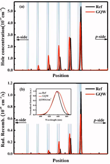
tions. Figure 1 shows the simulated hole distribution and radiative recombination distribution along MQWs at 100 A/cm2. For reference LED structure, it can clearly be
seen that holes mostly concentrate in the QW nearest p-side 共denoted as the first QW兲, so does the radiative recombina-tion. This phenomenon coincides with the optical measure-ment result in Ref.16, which is mainly due to poor transpor-tation of holes. While in the case of GQW LED structure, the hole concentration decreases in the first QW by about 16%, but increases in the second, third, and fourth QWs by 7%, 94%, and 175%, respectively, as compared with reference LED. It indicates that the holes are more capable of trans-porting across the first QW, consisted with our hypothesis. On the other hand, electrons are relatively not being affected due to their high mobility. Therefore, more wells will partici-pate in the recombination process, as illustrated by the radia-tive recombination distribution in Fig.1共b兲. Accordingly, the simulated EL spectrum of GQW LED at current density of 100 A/cm2 exhibits lager full width at half maximum 共FWHM兲 than that of reference LED, as shown in the inset of Fig.1共b兲. Moreover, due to the relative low carrier densi-ties in the first QW and more uniform of carrier distribution, the possibility of Auger scattering and carrier overflow can be lower. And the alleviation of efficiency droop can be expected.
Figure2 shows the power-dependent EL average wave-length and FWHM of reference and GQW LED at room
temperature. The EL measurement was performed by on-wafer probing with a spectrometer. The emission wavelength 共457.7 nm at 1 A/cm2兲 and FWHM 共21.9 nm at 1 A/cm2兲
for GQW LED are larger than those for reference LED 共448.5 nm and 17.9 nm兲, respectively. It could be due to the graded-thickness and wider wells near to p-side in GQW. Besides, as increasing the injection current from 1 to 100 A/cm2, EL spectrum for GQW LED exhibits significant
blueshift of 21.8 nm and broadening of about 11.6 nm, com-pared with 12.6 nm and 8.2 nm, respectively, for reference LED. Generally, the blueshift of the GaN-based LED can be attributed to the band filling effect in localized states and the charge screening effect of quantum confined Stark effect 共QCSE兲.17
And the broadening of FWHM is mainly due to the band filling effect and self-heating effect. In GQW and reference LEDs, the band filling effect and self-heating effect can be considered to be equivalent because they have the same indium content and total volumes of active region. Thus, there must be other reasons for such significant blue shift and broadening of EL spectra in GQW LED.
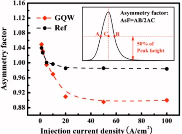
According to the simulated results mentioned above, more holes distribute in the narrower wells in GQW LED structure. Once more carriers radiatively recombine in nar-rower wells, the intensity of shorter-wavelength part in emis-sion spectrum will rise. Thus, changes in symmetry of spec-trum could be expected. To investigate the symmetry of EL spectrum in detail, the asymmetry factor 共AsF兲 was calcu-lated. As illustrated the inset of Fig. 3, it can be defined as the distance from the center line of the peak to the back slope 共AB兲 divided by twice the distance from the center line of the peak to the front slope 共2AC兲, with all measurements made at 50% of the maximum peak height. The calculated AsF under every injection level for both samples are sum-marized in Fig. 3. It can clearly be seen that, AsF of refer-ence LED decreases slightly from 1.04 to be about 0.98 when injection current increases from 1 to 100 A/cm2.
While GQW LED shows larger variation, the AsF starts at 1.05 共0.1 A/cm2兲 and saturates at about 0.89 共after
20 A/cm2兲. According to the definition of AsF, if the bluer
light emits from narrower wells, the symmetry of spectrum would be interrupted and smaller than 1. Therefore, we can conclude that GQW does have superior radiative recombina-tion distriburecombina-tion, which leads to the EL spectrum blueshifts and broadens significantly with increasing the injection cur-FIG. 1. 共Color online兲 Simulated 共a兲 hole distribution and 共b兲 radiative
recombination distribution in reference and GQW LEDs.
FIG. 2. 共Color online兲 Average wavelength and FWHM as a function of current density for reference and GQW LEDs.
181101-2 Wang et al. Appl. Phys. Lett. 97, 181101共2010兲
This article is copyrighted as indicated in the article. Reuse of AIP content is subject to the terms at: http://scitation.aip.org/termsconditions. Downloaded to IP: 140.113.38.11 On: Wed, 30 Apr 2014 09:56:33
rent. These enormous changes in wavelength and linewidth might make the design of the GQW concept impractical for lighting applications. In the future, we will optimize the GQW structure, such as appropriately reducing the indium content of the wider wells, to alleviate these effects.
Finally, we investigated the efficiency droop behaviors in both LEDs. The output powers measured with a calibrated integrating sphere and the normalized efficiency共兲 of ref-erence and GQW LED are plotted in Fig.4as a function of injection current density. The light output power of GQW LED is found to be enhanced by 35% at 20 A/cm2, as
com-pared with the reference LED 共24.3 mW versus 18.0 mW兲. This indicates that even with wider wells共worse wave func-tion overlap for electrons and holes兲 near p-side, the overall efficiency for GQW LED is still higher than reference, and the utilization rate of MQWs is improved. More importantly, the maximum efficiency 共peak兲 of GQW LED appears at
injection current density of 30 A/cm2, which is much higher than that for reference LED 共at 2 A/cm2兲. And the
effi-ciency droop, defined as 共peak-200 A cm2兲/peak, is
allevi-ated from 32% in reference LED to 16% in GQW LED. This improvement could be mainly attributed to the superior hole distribution and radiative recombination distribution, and also the reduction of Auger scattering resulting from the lower carrier concentration in QW nearest p-side.
In conclusion, InGaN/GaN LEDs with graded-thickness multiple quantum wells were investigated both experimen-tally and numerically. The APSYS simulations indicate that superior hole distribution can be achieved in the GQW de-signed MQWs, in which the well-thickness increases along 关0001兴 direction. It might be attributed to the longer radiative recombination lifetime in the wider well nearest to p-type layer. Moreover, by analyzing the EL spectra in detail, the additional emission from the narrower wells were demon-strated. This indicates that more carriers distribute in the pre-vious wells, which agrees well with the simulated results. As a result, the efficiency droop behavior was alleviated from 32% in reference LED to 16% in GQW LED. In addition, the light output power was enhanced from 18.0 to 24.3 mW at 20 A/cm2compared to reference LED with the same active volume. This work implies that with suitable active region design, carrier transportation behavior could be modified, which is very useful for alleviating efficiency droop.
The authors would like to thank Dr. T. C. Hsu and Dr. M. H. Shieh of Epistar Corporation for their technical support. This work was funded by the National Science Council in Taiwan under Grant No. NSC NSC98-3114-M-009-001.
1M. H. Kim, M. F. Schubert, Q. Dai, J. K. Kim, E. F. Schubert, J. Piprek, and Y. Park,Appl. Phys. Lett. 91, 183507共2007兲.
2K. J. Vampola, M. Iza, S. Keller, S. P. DenBaars, and S. Nakamura,Appl. Phys. Lett. 94, 061116共2009兲.
3K. Ding, Y. P. Zeng, X. C. Wei, Z. C. Li, J. X. Wang, H. X. Lu, P. P. Cong, X. Y. Yi, G. H. Wang, and J. M. Li,Appl. Phys. B: Lasers Opt. 97, 465
共2009兲.
4C. H. Wang, J. R. Chen, C. H. Chiu, H. C. Kuo, Y. L. Li, T. C. Lu, and S. C. Wang,IEEE Photon. Technol. Lett. 22, 236共2010兲.
5A. David and M. J. Grundmann,Appl. Phys. Lett. 96, 103504共2010兲. 6B. Monemar and B. E. Sernelius,Appl. Phys. Lett. 91, 181103共2007兲. 7M. F. Schubert, J. Xu, J. K. Kim, E. F. Schubert, M. H. Kim, S. Yoon, S.
M. Lee, C. Sone, T. Sakong, and Y. Park,Appl. Phys. Lett. 93, 041102
共2008兲.
8Y. K. Kuo, J. Y. Chang, M. C. Tsai, and S. H. Yen,Appl. Phys. Lett. 95, 011116共2009兲.
9R. A. Arif, Y. K. Ee, and N. Tansu,Appl. Phys. Lett. 91, 091110共2007兲. 10S. C. Ling, T. C. Lu, S. P. Chang, J. R. Chen, H. C. Kuo, and S. C. Wang,
Appl. Phys. Lett. 96, 231101共2010兲.
11J. Xie, X. Ni, Q. Fan, R. Shimada, Ü. Özgür, and H. Morkoç,Appl. Phys. Lett. 93, 121107共2008兲.
12X. Ni, Q. Fan, R. Shimada, Ü. Özgür, and H. Morkoç,Appl. Phys. Lett.
93, 171113共2008兲.
13C. K. Sun, S. Keller, T. L. Chiu, G. Wang, M. S. Minsky, J. E. Bowers, and S. P. DenBaars, IEEE J. Sel. Top. Quantum Electron. 3, 991共1997兲. 14R. Charash, P. P. Maaskant, L. Lewis, C. McAleese, M. J. Kappers, C. J.
Humphreys, and B. Corbett,Appl. Phys. Lett. 95, 151103共2009兲.
15F. Bernardini, in Nitride Semiconductor Devices: Principles and Simula-tion, edited by J. Piprek共Wiley, New York, 2007兲, pp. 49–67.
16A. David, M. J. Grundmann, J. F. Kaeding, N. F. Gardner, T. G. Mihopou-los, and M. R. Krames,Appl. Phys. Lett. 92, 053502共2008兲.
17T. Takeuchi, S. Sota, M. Katsuragawa, M. Komori, H. Takeuchi, H. Amano, and I. Akasaki,Jpn. J. Appl. Phys. 36, L382共1997兲.
FIG. 3.共Color online兲 Current-dependent asymmetry factor of EL spectra of reference and GQW LEDs.
FIG. 4. 共Color online兲 Comparison of normalized EL efficiency and L-I curves.
181101-3 Wang et al. Appl. Phys. Lett. 97, 181101共2010兲
This article is copyrighted as indicated in the article. Reuse of AIP content is subject to the terms at: http://scitation.aip.org/termsconditions. Downloaded to IP: 140.113.38.11 On: Wed, 30 Apr 2014 09:56:33