行政院國家科學委員會專題研究計畫 成果報告
矽奈米場效電晶體及氧化層奈米線: 理論,實驗,及應用潛
力(3/3)
計畫類別: 個別型計畫
計畫編號: NSC93-2215-E-009-002-
執行期間: 93 年 08 月 01 日至 94 年 07 月 31 日
執行單位: 國立交通大學電子工程研究所
計畫主持人: 陳明哲
計畫參與人員: 呂明霈,李建志,顏士貴,曾貴鴻,蔡鐘賢
報告類型: 完整報告
處理方式: 本計畫可公開查詢
中 華 民 國 94 年 10 月 31 日
行政院國家科學委員會補助專題研究計畫成果報告
※※※※※※※※※※※※※※※※※※※※※※
※
矽奈米場效電晶體及氧化層奈米線: 理論,實驗及應用潛力(3/3)
※
※※※※※※※※※※※※※※※※※※※※※※※
計畫類別:▓個別型計畫 □整合型計畫
計畫編號:
NSC 93-2215-E-009-002-
執行期間:
93/08/01 ~ 94/07/31
計畫主持人:陳明哲
計畫參與人員:呂明霈,李建志,顏士貴,曾貴鴻,蔡鐘賢
成果報告類型(依經費核定清單規定繳交):
□精簡報告 ▓完整報告
本成果報告包括以下應繳交之附件:
□赴國外出差或研習心得報告一份
□赴大陸地區出差或研習心得報告一份
□出席國際學術會議心得報告及發表之論文各一份
□
國際合作研究計畫國外研究報告書一份
處理方式:除產學合作研究計畫、提升產業技術及人才培育研究計畫、列管計畫
及下列情形者外,得立即公開查詢
□涉及專利或其他智慧財產權,□一年□二年後可公開查詢
執行單位:國立交通大學電子工程學系
中 華 民 國 94 年 10 月 31 日
行政院國家科學委員會專題研究計畫成果報告
矽奈米場效電晶體及氧化層奈米線: 理論,實驗及應用潛力(3/3)
Si NanoFET and Oxide Nanowire: Theory, Experiment, and
Potential Applications (3/3)
執行期限: 93/08/01 ~ 94/07/31
計畫編號: NSC 93-2215-E-009-002-
主持人:陳明哲教授 國立交通大學電子工程學系
一、中文摘要
本計劃為期三年,探索奈米場效電晶體 及氧化層奈米線之嶄新領域,在奈米場效電晶 體部份,以最先進製程製作奈米場效電晶體元 件,光罩閘極長度範圍 250 nm~20 nm,氧化 層厚度 5 nm~<1 nm。 進行電性量測及低溫 實驗。利用自行發展的量子力學模擬器與實驗 比較以萃取重要物理參數。改進傳統通道反向 散射理論之缺失,更新的版本能正確反映線性 區完整特性,臨界電壓定義清楚無誤,以及低 溫特性等。更新的通道反向散射理論將含有已 萃取的二維電子氣或二維電洞氣密度等,並表 達為通道長度,氧化層厚度,閘電壓及汲極電 壓之函數。也進行應用潛力之研究:(1)萃取 載子速度分布以具體闡明載子速度超越;(2) 預測閘極長度縮小至極限時彈道傳輸限制並 與文獻比較;(3)預測長通道(250 nm)遷移 率變化引至推動電流變化百分比(可與矽鍺通 道製程之測試數據比較);(4)表現與溫度無 關之奈米場效元件;(5)開發 Spice 電路模擬 器專用的更新通道反向散射奈米場效電晶體 模式;(6)晶片電路實現包括低溫電路;以及 (7)其它應用潛力之發掘。 在氧化層奈米線部分,將發展自動化奈 米線產生控制程式,一旦氧化層奈米線形成, 即進行電性量測(低電壓的範圍)。也量測時 域之電報雜訊,頻域之低頻雜訊特性,以及低 溫下的實驗量測。利用量子點接觸理論模式與 實驗比較,萃取相對應的參數。並發展出量子 點接觸之電報雜訊版本,低頻雜訊版本以及低 溫版本,也與實驗一一比較並萃取參數。亦進 行應用潛力之研究:(1)開發更為快速的奈米 線產生設備或產生電路;(2)因與矽的製程完 全相容,將包含其他傳統的矽元件以產生功能 電路如負電阻,階梯狀特性等;(3)利用所量 測到的低溫參數設計奈米線低溫電路;(4)在 小面積下或在低溫下應能表現出類似單電子 電晶體之特性;以及(5)其他應用潛力之發 掘。 關鍵詞:矽,奈米,場效電晶體,氧化層,奈米線, 散射,低溫,彈道傳輸,電報雜訊,低頻雜訊,量 子點接觸,單電子電晶體。英文摘要
This is a three-years project to explore new areas of nanoFET and oxide nanowire. In the nanoFET side , state-of-the-art process technologies are used for manufacturing nanoFETs with mask gate length ranging from 250 nm down to 20 nm and gate oxide thicknesses from 5 nm to less than 1 nm,then followed by I-V/C-V measurement as well as low temperature experiment. Our developed quantum mechanical I-V/C-V simulators are used to compare experimental data from which relevant physical parameters are extracted. Improved channel backscattering theory including two-dimensional electron or hole gas is expressed as a function of temperature,channel length,oxide thickness,gate voltage,and drain voltage. Also carried out are promising potentials :( 1 ) extract carrier velocity profile in order to highlight velocity overshoot ;( 2 ) predict ballistic limit as channel length is reduced down to extremity along with literature comparison;(3)predict device drive current change due to mobility change(compare data from strained-Silicon or Si-Ge channel process);(4)implementation of
nanoFETs having less temperature dependencies ;( 5 ) update SPICE models to account for improved channel backscattering in nanoFETs ;( 6 ) realization of integrated circuits including low temperature circuits; and (7)exploration of other applications.
In the oxide nanowire side,we will develop an automatic electrical control program for nanowire generation in gate oxide films. Once a nanowire is created therein , low-voltage I-V’s are measured. Also performed are random telegraph signal in time domain,low frequency noise in frequency domain,and low temperature experiment. Quantum point contact model is used to compare data in order to extract physical parameters. We will develop out random telegraph signal version,low frequency noise version,and low temperature version of channel back scattering theory , as well as experimental comparison and parameter extraction. We also examine potential applications:(1)develop fast equipment or circuits for nanowire generation;(2)owing to 100% compatibility with current silicon processes,combine other conventional silicon devices to constitute functional circuits with novel features like negative resistance and step-like current;(3)apply low temperature data and parameters to design and realize low temperature circuits;(4)under small area or low temperature conditions,expect nanoFETs to show behaviors of single electron transistors ; and ( 5 ) explore other applications.
Key Words:Silicon,nano,FET,oxide,MOS, nanowire , scatter , low temperature , random telegraph signal,low frequency noise,quantum point contact,single electron transistors
二、緣由與目的
1.
近年來隨著 Si MOSFET 元件的持續不斷 縮小, 其有效通道(channel)長度(等於 mask gate length 光罩閘極長度減去 Source/Drain overlap 長度)已經達到奈米級的尺寸,可與平均自由路徑 (mean-free-path)相當甚至更小,在此情況下,傳 統的載子遷移率(mobility)已無意義,因其在如此 超短通道內遭遇極為微少的碰撞(collision),故 必得以量子力學即波(wave)的觀點去闡釋並處理 相關問題。普渡大學的 Datta 教授與 Lundstrom 教 授所提出的通道背向散射理論(Channel Backscattering Theory)特別突出,尤能處理像載 子速度超越(Carrier Velocity Overshoot),彈道 傳輸限制(Ballistic Transport Limit)等爭議性
極高的問題,吸引全球目光。MIT 的 Antoniadis 教 授利用通道背向散射理論在載子速度這議題上有 傑出的表現,IBM 的 Yuan Taur 博士 (現加大教授) 在蒙地卡羅模擬及實驗上證明可與通道背向散射 理論銜接。
至於通道背向散射理論應用潛力,本研究群堅 信:
1. 目前電路模擬器 SPICE 所用之 Device Models 係基於載子之 Drift 及 Diffusion(也即 mobility) 行為而來,不適用於奈米 FET 元件。因之能以波動 處 理 通 道 傳 輸 特 性 之 背 向 散 射 理 論 應 可 為 奈 米 FETs 元 件 特 性 模 式 之 用 以 取 代 SPICE 中 元 件 Drift-Diffusion 版本。 2. 波動或透納(Tunneling)行為基本上為量子傳 輸應有與溫度無關的特性,因之奈米 FETs 元件表 現出與溫度無關的特性應可期待。 通道背向散射理論亦牽涉到 Subbands 上二維 電 子 氣 (2DEG) 或 二 維 電 洞 氣 (2DHG) 的 Quantum Confinement 效應。本研究群這幾年已自行發展出 量 子 力 學 (Quantum Mechanics) I-V/C-V 模 擬 器 (已算入 2DEG 及 2DHG),亦對波的入射及反射行為 鑽研至深。而基於奈米 FET 元件日趨重要,相關的 傳導機制必須釐清且應用潛力有待發掘及推廣,本 實驗室基於在此領域有良好研究基礎,特別提出此 一研究計畫。 本計畫亦探討閘極介電層 percolation 路徑 (截面積約 1nm2, 長度約為介電層厚度)的奈米線 nanowire-like 行為, 最近 Spain Sune 教授 group 提出 Quantum point contact 理論模式成功闡釋此 nanowire 行為。Percolation 路徑自身亦表現出 on-off switching 或 RTS(Random Telegraph Signal; 電報雜訊)現象, 甚至閘極介電層內有二 條 percolation 路徑或 nanowires,彼此之間產生詭 異的 on-off switching 現象, Sune 教授亦認為 percolation 路徑的 nanowire 行為可為未來元件候 選人之一, 且有一大優勢:與現有 Silicon CMOS 製 程完全相容, 問題是該如何實現。本研究群這幾年 在閘極氧化層 percolation 路徑的理論模式實驗已 作出好的研究, 我們並且觀察到 nanowire 在頻域 的 Lorentzian noise(相當於時域的 RTS 現象), 並 很清楚如何從電性上產生 percolation nanowire 且不致因隨後的大電流進入而產生的熱能造成鉅 大 的 結 構 破 壞 。 我 們 亦 要 研 究 percolation nanowire 在低溫下的巨觀及微觀行為特性, 希冀 能 觀 察 到 前 人 未 見 者 並 提 供 更 多 的 設 計 參 數 。 Percolation nanowire 的應用潛力也將具體地提出 及製程實現。
三、研究方法與成果
1.(
通道背向散射
)
channel backscattering coefficients into two distinct components: Mean-free-path and KT layer width, as shown in the published articles (2004 IEEE TED and
2005 Silicon Nanoelectronics Workshop, for example).
2.
(
奈米系統的雜訊與擾動
)
Coulomb energy is essential to the charging of a nanometer-scale trap in the oxide of a metal-oxide-semiconductor (MOS) system. Traditionally the Coulomb energy calculation was performed on the basis of an interface-like trap. In this paper, we present for the first time experimental evidence from a 1.7-nm oxide: substantial enhancements in Coulomb energy due to the existence of a deeper trap in the oxide. Other corroborating evidence is achieved using a multiphonon theory, which can adequately elucidate the measured capture and emission kinetics. The corresponding configuration coordinate diagrams are established. Then we elaborate on the clarification of the Coulomb energy and differentiate it from that in memories containing nanocrystals or quantum dots in the oxide. Eventually, some critical issues encountered are addressed as well.
3.
(
奈米線
)
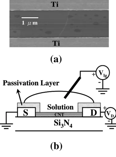
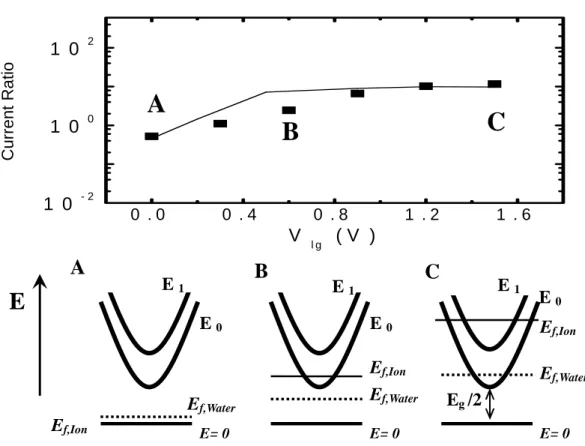
We fabricate and measure a single-walled carbon nanotube transistor having a liquid-gate electrode. The ratio value of Ion/Ioff is as high as 104, indicating the
presence of a semiconducting channel. A passivation layer over the source/drain electrode greatly suppresses the liquid-gate leakage by about three orders of magnitude. The channel currents are noticeably distinct between two liquid samples: distilled water and aqueous solution (1×10⁻⁴ M NaCl). This biological sensing ability is attributed to the different electrical double-layer capacitances with respect to the bulk part of the channel. The corresponding theoretical calculation is carried out in detail.
四、 結論與討論
1. 在奈米系統的雜訊與擾動領域當中我們確實 已作出世界級的貢獻:
(a) 一篇送至Physical Review - B 的論文獲致兩 位 國 際 評 審 的 高 度 推 薦 (well written, high quality, new data, novel linkage to quantum dots in a MOS system, and interesting and useful analysis)
(b) 一篇 Applied Physical Letters (M. J. Chen and M. P. Lu, APL, vol. 81, p. 3488, 2002) 論 文先後被 德國漢堡大學 Schroeder 教授 及 希臘 雅典大學 Varotsos 教授 於他們的APL and PRL 論 文引用:
2. 我們已將奈米線研究延伸至奈米碳管電晶體 測試鍵, 完成一篇 Applied Physical Letters 探 討生物樣本電性量測及量子力學理論計算, 特別 是後者確實 interesting and useful 且為APL 國 際 評 審 高 度 認 定 , APL 編 輯 最 近 的 回 應 是 : Considerable for publication.
3. 最後在通道背向散射領域, 我們確實完成了 大 量 的 實 驗 工 作 , 也 有 一 些 論 文 發 表 並 被 引 用 (部分見下). 然而每當我們自以為接近成功的一 步, 我們就愈發覺現有的通道背向散射理論架構 有所不足, 是以計畫雖然結束我們仍繼續肇清通 道背向散射理論架構, 作法是運用 Monte Carlo 技 巧, 到目前為止已見若干突破, 假以時日 (約需 數月) 我們定能在此嶄新領域取得國際性地位.
參考文獻:
1. M. J. Chen, H. T. Huang, Y. C. Chou, R. T. Chen, Y. T. Tseng, P. N. Chen, and C. H. Diaz, “Separation of channel backscattering coefficients in nanoscale MOSFETs,” IEEE Trans. Electron
Devices, vol. 51, pp. 1409-1415, September 2004.
2. M. P. Lu and M. J. Chen, “Anomalous behaviors of random telegraph signals in ultra-thin gate oxide MOSFETs,” SSDM, pp. 408-409, September 2004. (Tokyo)
3. M. J. Chen, R. T. Chen, and Y. S. Lin, “Decoupling channel backscattering coefficients in nanoscale MOSFETs to establish near-source channel conduction-band profiles,” Silicon
Nanoelectronics Workshop, pp. 50-51, June 2005. (Kyoto)
4. M. P. Lu, C. Y. Hsian, P. Y. Lo. J. H. Wei, Y. S. Yang, and M. J. Chen, “Semiconducting single-walled carbon nanotubes exposed to distilled water and aqueous solution: electrical measurement and theoretical calculation,” Applied Physics Letters, 2005 (under review for months, now approaching with positive results) 5. M. P. Lu and M. J. Chen, “Oxide trap enhanced Coulomb energy
in a metal-oxide-semiconductor system,” Physical Review - B, 2005 (under review for months, now approaching with positive results).
Figures:
(cited by a 2004 IEDM paper)
0 20 40 60 0.050 0.051 0.052 Tim e (sec) | I S | ( µ A) W /L=0.6 µm /0.07 µm VG= 0.2 V 0.150 0.152 0.154 0.156 | I S | ( µ A) VG= 0.25 V 0.384 0.388 0.392 0.396 | I S | ( µ A) VG= 0.3 V
0.2
0.3
0.4
10
-110
010
110
2τ
c/
τ
eV
G(V)
Exp. W/L=0.1 µm /0.16 µm Exp. W/L=0.6 µm /0.07 µm Eox-ET= 3.3 eV , ZT= 0 nm Eox-ET= 3.2 eV , ZT= 0.7 nm0.0
0.1
0.2
0.3
0.4
0.5
0.0
0.2
0.4
0.6
0.8
1.0
Qinv Qdep Normal ized Ima ge Charge VG (V) Tox = 1.7 nm ZT= 0 nm ZT= 0.3 nm ZT= 0.7 nm QG 0.0 0.1 0.2 0.3 0.4 0.5 0.10 0.15 0.20 0.25 0.30 C ou lomb En ergy (e V ) VG (V) Tox = 1.7 nm ZT= 0 nm ZT= 0.3 nm ZT= 0.5 nm ZT= 0.7 nm 1010 1011 1012 0.0 0.2 0.4 0.6 0.8 1.0 1.2 Qinv Norm al iz ed I m age Charge ns ( c m-2 ) TOX= 1 nm TOX= 2 nm TOX= 5 nm QG10
1010
1110
120.0
0.2
0.4
0.6
0.8
1.0
1.2
1.4
Qinv Q G N orma liz ed Im age Ch arge ns ( c m-2 ) ZT= 0 nm @ Tox = 1 nm ZT= 0.5 nm @ Tox = 1 nm ZT= 0 nm @ Tox = 5 nm ZT= 0.5 nm @ Tox = 5 nm Fig. 1 Schematic cross section of thedevice showing the capture-emission process.
Fig. 2 The measured fluctuations simultaneously occurring in both source and drain currents.
Fig. 3 The measured RTS recorded as a function of gate voltage.
Fig. 4 The measured (symbols) and calculated (lines) ratio of the mean capture time (τc) divided by the mean emission time (τe) against gate
voltage for two devices. The inset shows underlying band diagram indicating the trap position.
Fig. 5 The measured RTS amplitude versus gate voltage for two devices.
Fig. 6 A capacitive coupling model taking the effect of the trap depth into account.
Fig. 7 The image charge on the gate, the inversion layer, and the depletion region versus gate voltage for different trap depths.
Fig. 10 The image charge versus inversion layer carrier density for different oxide thicknesses and different trap depths.
G V +
n
−n
+ e D V D I S I type p− G V +n
−n
+ e D V D I S I type p− 0 4 8 12 16 20 0.260 0.264 ID ( µ A) Time (sec) 0 4 8 12 16 20 -0.264 -0.260 IS ( µ A) W/L=0.1 µm /0.16 µm VG= 0.3 V VD= 10 mV 0.1 0.2 0.3 0.4 0.5 0 2 4 6 ∆ I/I ( % ) VG (V) Exp. W/L=0.1 µm /0.16 µm Exp. W/L=0.6 µm /0.07 µm Ground oxC
depC
invC
GV
q − G Q dep Q inv Q T Z oxT
Ground oxC
depC
invC
GV
q − G Q dep Q inv Q T Z oxT
T ox E E− ' 0 E 0 E ox T substrate Si Oxide T Z T ox E E− ' 0 E 0 E ox T substrate Si Oxide T ZFig. 11 (a) Topside view of the CNT FET testkey and (b) its measurement setup.
S
D
Si
3
N
4
Passivation Layer
V
DV
lgSolution
+
+
-CNTS
D
Si
3
N
4
Passivation Layer
V
DV
lgSolution
+
+
-CNT(a)
(b)
1 μm
Ti
Ti
1 μm
Ti
Ti
A
B
C
E
f,IonE
f,WaterE
f,IonE
f,WaterE
C
B
A
E
0E
1E
1E
1E
0E
0 0 . 0 0 . 4 0 . 8 1 . 2 1 . 61 0
- 21 0
01 0
2 Cu rr en t R a tioV
l g( V )
E
g/2
E
f,WaterFig. 12 Theoretical Calculation and Measurement Results corresponding to Fig. 11.
E= 0 E= 0
E= 0