國
立
交
通
大
學
電機與控制工程學系
碩
士
論
文
減少等效串聯電感效應且不須等效串聯電阻補償的
固定導通時間控制直流直流降壓轉換器
Reduction of Equivalent Series Inductor Effect in Constant On-Time
Control DC-DC Converter without ESR Compensation
研 究 生:賴王為
指導教授:陳科宏 博士
減少等效串聯電感效應且不須等效串聯電阻補償的固定導通時
間控制直流直流降壓轉換器
Reduction of Equivalent Series Inductor Effect in Constant On-Time
Control DC-DC Converter without ESR Compensation
研 究 生:賴王為 Student:Wang-Wei Lai
指導教授:陳科宏 Advisor:Ke-Horng Chen
國 立 交 通 大 學
電 機 控 制 工 程 學 系
碩 士 論 文
A Thesis
Submitted to Department of Electrical and Control Engineering
College of Electrical Engineering
National Chiao Tung University
in partial Fulfillment of the Requirements
for the Degree of
Master
in
Electrical and Control Engineering
October 2010
Hsinchu, Taiwan, Republic of China
中華民國九十九年十月
i
減少等效串聯電感效應且不須等效串聯電阻補償的固定導通時
間控制直流直流降壓轉換器
研究生:賴王為 指導教授:陳科宏博士
國立交通大學電機與控制工程研究所碩士班
摘 要
隨著可攜式產品的需求逐漸增加,用來提供可攜式產品系統電源且具有高效 能以及小體積的電壓穩壓器變得越來越重要。常見於實際應用的固定導通時間控 制法電壓穩壓器具有幾項優點,如快速暫態反應、系統結構簡單,以及在輕負載 時具有高效率的優點。一般來說,固定導通時間控制法穩壓器是利用輸出端訊號 的漣波來穩壓,但是傳統的控制法使用具有小等效串聯電阻的輸出電容時,由於 輸出端訊號的漣波僅有電容的成分,故漣波很小系統易受雜訊影響。因此傳統上 須使用大等效串聯電阻的輸出電容才可有效控制系統。 本文提出之固定導通時間直流轉換器不須使用等效串聯電阻補償且可消除輸 出電容上的等效串聯電感效應。此外快速暫態反應與小電壓降變化皆可達成。並 且由於導通時間可隨輸入及輸出電壓調整,操作在連續導通模式時的系統切換頻 率可以在廣泛的輸入電壓裡維持幾乎定值。模擬結果顯示出輸出電壓漣波維持小 於 5 mV,在負載變動範圍為 500 mA 時輸出電壓的回復時間小於 10 μs。此時 使用的等效串聯電阻小於 5 mΩ。ii
Reduction of Equivalent Series Inductor Effect in Constant On-Time Control
DC-DC Converter without ESR Compensation
Student: Wang-Wei Lai Advisor: Dr. Ke-Horng Chen
Department of Electrical and Control Engineering
National Chiao-Tung University
Abstract
With the growing demand of portable devices, voltage regulators which have high performance and compact size become more important to provide system power. Constant on-time control regulators are preferred in practice for some important advantages, such as fast response time, simple system structure and good efficiency for light load. In general, constant on-time control regulators regulate their output voltage based on the ripple component in the output signal. However, in conventional constant on-time control with small ESR value on the output capacitor, the regulator is easily affected by the noise due to small output ripple, which is dominated by the ripple on the output capacitor. Thus, for constant on-time control regulators, an output capacitor with a large ESR has to be used so that effective ripple control can be realized.
The proposed constant on-time control DC-DC converter removes the need of conventional equivalent series resistor (ESR) compensation and simultaneously aims to eliminate equivalent series inductor (ESL) effect of the output capacitor. Besides, fast transient response and small dip voltage variation can be achieved. Furthermore, since the on-time period is set simply by input and output voltages, the switching frequency in continuous conduction mode (CCM) operation is relatively constant over a wide input voltage range. Simulation results show that the output ripple and the recovery time keep smaller than 5mV and 10μs, respectively, when load current step is 500mA and ESR is smaller than 5mΩ.
iii
誌 謝
首先要感謝我的指導老師陳科宏博士,有老師在這兩年多來的細心指導,才得以 讓這篇論文順利的完成。在研究所的這兩年多,老師教導我許多電路上的知識,以及 作電路的技巧,充實了我許多的專業知識。此外,平時還會教導我許多待人處事的道 理,讓我的知道在畢業之後如何在社會上立足。非常感謝老師在研究所時期的諄諄教 誨。 同時要感謝實驗室的小乖、輝哥、小契、小菜、國林學長,在我研究遇到困難時, 都會細心解惑,分享了許多坐電路的經驗,讓我受益良多。接著,要感謝小瑛瑛、小 群群、五點、士偉,你們在我求學過程中,一起討論、一起研究,在研究之餘,也一 起玩樂,有了你們陪伴,讓我的研究所回憶增添不少色彩,感謝你們。再來,要感謝 Lab 912 的學長、同學以及學弟妹們,有了你們的幫助,讓我在實驗室研究順利。 感謝我的女友雅萍,對我的支持與包容,以及在實驗室的陪伴,在繁雜的課業以 及研究進度下,讓我減輕許多壓力,才得以繼續朝目標努力,順利的畢業,往下個目 標邁進。最後要感謝我的父母,以及家人,有了你們的支持與關心,讓我無憂無慮地 作研究,專心在課業上的進度,感謝你們。 謹以此篇論文獻給我身邊的每位好朋友。iv
Contents
Chapter 1 ... 1
Introduction ... 1
1.1 Power Management System ... 1
1.2 Classification of Voltage Regulators ... 3
1.2.1 Linear Regulator ... 3 1.2.2 Charge Pump ... 5 1.2.3 Switching Regulator ... 6 1.2.4 Comparison ... 7 1.3 Motivation ... 8 1.4 Thesis Organization ... 10 Chapter 2 ... 11
Basic Knowledge of Switching Regulator ... 11
2.1 Performance Specification of Switching Regulator ... 11
2.1.1 Losses and Efficiency ... 12
2.1.2 Load and Line Regulation ... 14
2.1.3 Transient Response ... 15
2.2 Modulation Technologies ... 18
2.2.1 Pulse Width Modulation (PWM) ... 18
2.2.2 Pulse Frequency Modulation (PFM) ... 19
2.3 Descriptions of Ripple-Based Control Methods ... 21
2.3.1 Hysteretic Control Method ... 21
2.3.2 Constant On-time Control Method ... 23
2.3.3 Constant Off-time Control Method ... 25
Chapter 3 ... 27
Topology of Constant On-time Control DC-DC Buck Converter without ESR Compensation ... 27
3.1 System Stability Analysis of Conventional Constant On-time Control 27 3.2 Topology of the Proposed System ... 33
Chapter 4 ... 36
Circuit Implementation ... 36
4.1 Zero ESR Compensation Circuit ... 36
4.2 On-Time Timer ... 38
v
Chapter 5 ... 42
System of Reduction of Equivalent Series Inductor Effect in Constant On-Time Control DC-DC Converter without ESR Compensation Simulation Results, Conclusions and Future Work ... 42
5.1 Simulation Results ... 42
5.2 Conclusions ... 47
5.3 Future Work ... 48
vi
Figure Captions
Fig. 1. Energy constrained operation. ... 2
Fig. 2. Power management system. ... 3
Fig. 3. The basic structure of linear regulator. ... 4
Fig. 4. The basic structure of charge pump. ... 5
Fig. 5. The basic structure of buck type voltage mode switching regulator. . 7
Fig. 6. Transient waveform of VDS and ID curve in switching losses. ... 13
Fig. 7. The transient response of output voltage relates to load current. ... 16
Fig. 8. Pulse width modulation waveform. ... 18
Fig. 9. Analysis of conduction loss and switching loss at pulse width modulation. ... 19
Fig. 10. Pulse frequency modulation waveform. ... 20
Fig. 11. Analysis of conduction loss and switching loss at pulse frequency modulation. ... 21
Fig. 12. The block diagram of hysteretic control method. ... 23
Fig. 13. The block diagram of constant on-time control method. ... 24
Fig. 14. Inductor current and feedback voltage waveforms in DCM operation of constant on-time control. ... 25
Fig. 15. Inductor current and feedback voltage waveforms in DCM operation of constant off-time control. ... 26
Fig. 16. Small ESR caused double-pulse problem. ... 28
Fig. 17. Large ESL caused double-pulse problem. ... 30
Fig. 18. The noise effect on feedback voltage and power MOSFET switching signal. ... 31
Fig. 19. Enlarged waveform of feedback voltage and reference voltage that affected by noise. ... 32
Fig. 20. Topology of proposed constant on-time control DC-DC buck converter. 33 Fig. 21. The concept of the proposed technique. ... 34
Fig. 22. The operational scheme of the proposed technique. ... 35
Fig. 23. The proposed zero ESR compensation circuit. ... 37
Fig. 24. The on-time timer. ... 38
Fig. 25. The control logic circuit. ... 40
Fig. 26. Flow chart of control logic circuit. ... 41
Fig. 27. Chip layout. ... 43
Fig. 28. Waveforms of the output voltage and inductor current at different load current condition. (a) Iload =30mA (b) Iload =50mA (c) Iload =100mA. . 45
vii
Fig. 29. Transient response (a) when load current changes from 100mA to 600mA and (b) from 600mA to 100mA. ... 46
viii
Table Captions
TABLE I. COMPARISONS OF DIFFERENT TYPE REGULATORS. ... 8 TABLE II. DESIGN SPECIFICATIONS. ... 47
1
Chapter 1
Introduction
Portable devices such as cellular phones, laptops, and PDAs are widely used in today’s life. For the electronic device application, compact size and high performance voltage regulator plays an important role to provide system power. To extend the battery life of the battery-operated devices is the important issue for power management module in portable devices.
In this chapter, we will show the background and basic knowledge of power management system in chapter 1.1 firstly. The classification of power management circuits which including switching converters, linear regulators, and charge pump converters will show in chapter 1.2. The motivation will give in chapter 1.3. Finally, the thesis organization will show in chapter 1.4.
1.1 Power Management System
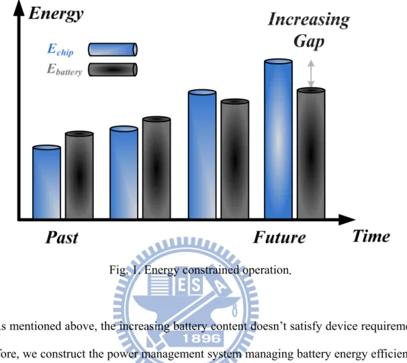
According to increasing demand for low-power multifunction system-on-a-chip (SOC), more and more functions are embedded in a device to meet the requirement. However, the growing of battery energy is not satisfied to chip requirement. As shown in Fig. 1, the growing of battery energy is not enough to supplying power of chips in the future. The running time of the portable devices, such as the lap tap, mobile phones and digital cameras, is a very important requirement for the consumers. Therefore, how to save the battery energy and use it more efficiently is the most important topic for power management system.
2
Fig. 1. Energy constrained operation.
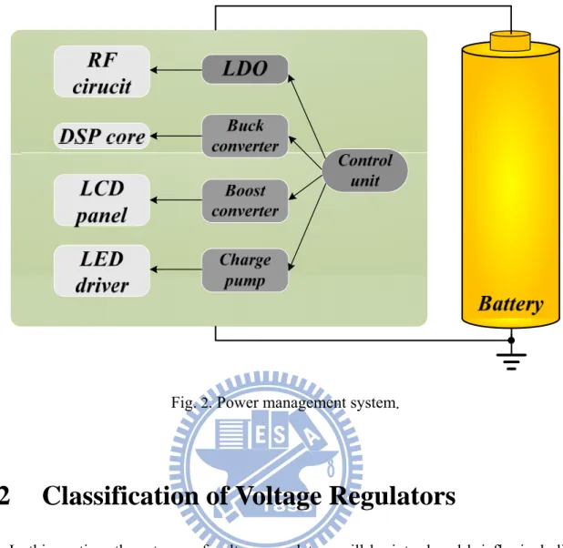
As mentioned above, the increasing battery content doesn’t satisfy device requirement. Therefore, we construct the power management system managing battery energy efficiently. As shown in Fig. 2, it may have many power devices for a mobile phone, which needs four regulated voltages, one buck converter for core micro processor, one boost converter for LCD panel, one charge pump for white LED driver and one Low-dropout (LDO) regulator for RF power amplifier [1]. The system of cell phone will operate in different modes, such as sleeping mode, communication mode and so on. And these blocks are only needed powered when the function are active. The control unit is used to control these block enable or disable, respectively. As a result, we can enhance system efficiency by using the control unit cell that decides the operational mode of power supply module.
3
Fig. 2. Power management system.
1.2 Classification
of
Voltage
Regulators
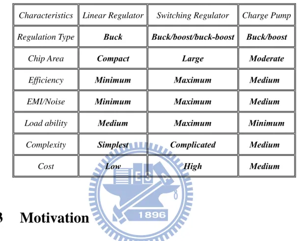
In this section, three types of voltage regulators will be introduced briefly, including linear regulators, switched capacitor circuits and switching regulators. Finally, a brief comparison will be given about three types of voltage regulators. The comparisons included circuit complexity, cost, efficiency, load ability and so on.
1.2.1 Linear Regulator
Linear regulator is also called LDO voltage regulator because there is a low drop-out voltage between input and output pin about 100~500mV [2]. LDO regulators are widely used as power management ICs in portable communication systems since they occupy a small chip area and can convert Li-Ion battery voltage to a low-noise and high-precision voltage to noise-sensitive analog blocks for ensuring high performance. The characteristic
4
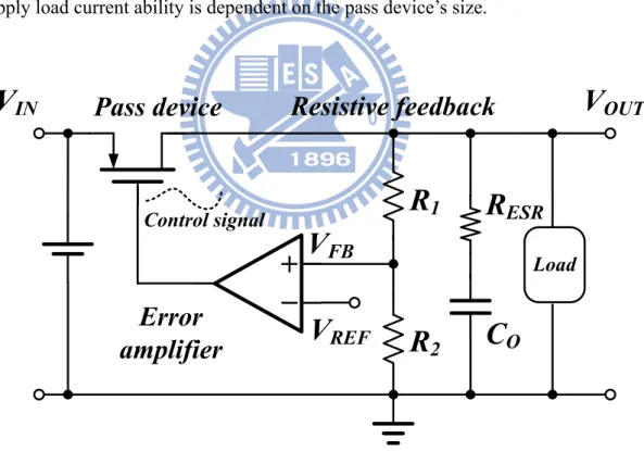
of LDO is compact without complex control unit, results in smaller chip size and cost. As shown in Fig. 3, the construction of LDO regulators usually utilizes a pass device, an error amplifier and a resistive feedback network. The pass device typically uses a p-type MOSFET for low dropout voltage. The error amplifier is used to regulate output voltage by controlling the pass device to supply load current. That is, LDO regulator utilizes the feedback network to construct shunt negative feedback effect to regulate output voltage. Therefore, LDO regulator does not need oscillation clock, then the output noise can be minimized and the output voltage does not have ripple. However, the disadvantage of this type regulator is the conversion efficiency, which is about the output voltage dividing input voltage. The highest efficiency occurs when output voltage is near input voltage. Besides, the supply load current ability is dependent on the pass device’s size.
V
OUTC
OR
1R
2V
REFV
IN Control signalError
amplifier
V
FB LoadR
ESRPass device
Resistive feedback
5
1.2.2 Charge Pump
The features of charge pump are described as follows [3] [4]. Firstly, the charge pump can be operated in both buck and boost mode, it depends on the reference voltage of the hysteric feedback control, but it is more efficiently in boost mode operation. Secondly, the circuit complexity of charge pump is between linear regulator and switching regulator. Thirdly, the electromagnetic interference (EMI) and switching noise problem are not heavier than switching regulator because of lower switching frequency. Finally, the load ability is weak because of output capacitor and switching frequency.
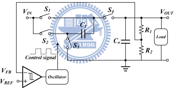
Fig. 4. The basic structure of charge pump.
Fig. 4 shows the basic structure of two phase charge pump regulator. It consists of four switches, two capacitors, one hysteric comparator, one oscillator and resistive feedback. The operation concept is charging and discharging the capacitor C1 in complementary phases.
Firstly, during phase Φ1, switches S1 and S3 are closed and switches S2 and S4 are opened,
6
switches S1 and S3 are opened and switches S2 and S4 are closed. Vin added the voltage on
capacitor C1 to charge output capacitor Co, so Co maintains an output voltage close to 2Vin.
With the hysteric feedback control, the output voltage level can be regulated at a desired value.
1.2.3 Switching Regulator
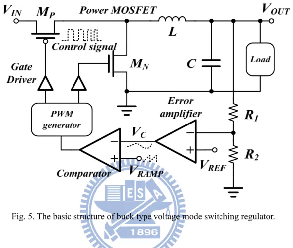
Switching regulators are mixed-signal circuits which have both analog and digital block in feedback loop. An analog signal which is error signal feeds back to produce a digital signal at a certain frequency rate which calls duty cycle. Output capacitor and inductors use duty cycle to regulate output voltage. The basic structure of buck type voltage mode switching regulator is shown in Fig. 5 [5]. The power stage of switching regulator consists of a couple of complementary power MOSFET (MP MN), passive storage elements inductor (L) and
capacitor (C) and resistive feedback network (R1 R2). Detailed operation is described as
follows; the resistors R1 and R2 sensing the variation of output voltage and error amplifier
receives the voltage variation information then brings the error signal (VC). The
comparator’s inputs receive the error signal from error amplifier and the ramp signal (VRAMP)
from ramp generator, then compares the quantity between the error signal and the ramp signal to decide the duty cycle. After generating the control signal, the PWM generator control the detail timing to avoid short through current. At last, the purposes of gate drivers are driving huge complementary power MOSFET.
Generally speaking, the conversion efficiency of switching regulator can achieve above 90% under heavy load condition. Meanwhile, with higher switching frequency in the range from hundreds of Kilo-Hertz to several Mega-Hertz, the storage components can be designed smaller to save the cost. But the EMI and noise problems become critical. The supply load
7
ability is the largest always in the range about hundreds of milliamps to several amps.
Fig. 5. The basic structure of buck type voltage mode switching regulator.
The characteristics of switching regulator are described as the following. Firstly, due to the storage components such as inductor and capacitor, the switching regulator can operate in three kinds of type including buck, boost and buck-boost mode. But the more external components cause the bigger PCB size and cost. Secondly, it suffers from EMI and switching noise problem due to switching based circuits.
1.2.4 Comparison
As the above description, three types of voltage regulator have its own advantages and disadvantages. How to choose the best voltage regulator as power supply depend on the electronic applications characteristics and specifications. The comparison of different type
8
voltage regulator is listed in TABLE I.
1.3 Motivation
The buck converters are widely used in portable devices to provide power from battery. In these applications, the DC-DC converter has to regulate the output voltage to lower voltage and must quickly respond to load current variation to keep the output voltage within a limited range. Conventional control methods for switching converter such as voltage-mode and current-mode control include the error amplifier, which is connected with frequency compensation network, to compensate for step changes in the load current. However, it leads to relatively slow response time and thus makes the switching converter hard to meet the load transient response requirement.
Switching converters using the output voltage ripple as the PWM ramp signal have been widely used to extend the battery life due to the simple control mechanism [6] [7].
TABLE I. COMPARISONS OF DIFFERENT TYPE REGULATORS.
Characteristics Linear Regulator Switching Regulator Charge Pump
Regulation Type Buck Buck/boost/buck-boost Buck/boost
Chip Area Compact Large Moderate
Efficiency Minimum Maximum Medium EMI/Noise Minimum Maximum Medium Load ability Medium Maximum Minimum
Complexity Simplest Complicated Medium
9
Besides, the response time of line and load transient is fast due to large control loop bandwidth. Its control method is usually called ripple-based control [8] [9]. Ripple-based control methods include hysteretic control, constant on-time control, and constant off-time control. The hysteretic control is widely used for buck converter to achieve a fast transient response, and the circuitry of the hysteretic control method is compact without complexity. But the major disadvantage of the hysteretic control is the noise effect on the output voltage ripple. This noise can prematurely terminate or initiate a switching period. Another drawback is the switching frequency is affected by parasitic parameters and can change a lot with different input and output voltage.
Constant on-time control operates at a relatively constant frequency without a oscillator due to the on-time period is set by input supply voltage and output voltage, and it does not require error amplifier and loop compensation network, leads to a fast line and load transient response due to its wide control bandwidth. For practical implementation, the equivalent series resistance (ESR) of the output capacitor can be used as the sensing resistor, which means the output voltage ripple including the current information. Moreover, the larger ESR value can reduce the noise effect on the output voltage ripple because of large output voltage ripple induced by ESR, but the unfavorably large overshoot/undershoot voltage in transient period comes from the use of large ESR. Therefore, in this thesis, a constant on-time control DC-DC converter without ESR compensation allows to use low ESR output capacitors, eliminating the need for ESR induced output ripple.
10
1.4 Thesis
Organization
The thesis introduces the basic knowledge of switching regulator in the Chapter 2. In the Chapter 3, the design and architecture of constant on-time control DC-DC converter without ESR compensation are presented. The internal overall circuit implementation and simulation results are shown in Chapter 4. Finally, the whole system chip simulation, system specification, conclusions and future work are presented in Chapter 5.
11
Chapter 2
Basic Knowledge of Switching
Regulator
In this chapter, the basic knowledge of switching regulator is presented. The characteristics and performance specification of switching regulator are shown in section 2.1. In section 2.2, the controlling modulator including pulse width modulation (PWM) and pulse frequency modulation (PFM) are introduced. Three kinds of ripple-based control method including hysteretic control, constant on-time control and constant off-time control are described in section 2.3.
2.1 Performance
Specification
of
Switching Regulator
Due to more and more electronics application need to be supplied by switching converter, the performances of switching converter have to be considered. The following are significant specifications of switching regulators. Firstly, the conversion efficiency of switching regulator is an important topic, how to keep high efficiency over wide loading range and loss analysis will be discussed in the section 2.1.1. The second part is excellent load and line regulation, the lower steady-state error of switching regulator will be discussed in the section 2.1.2. The final part is transient response, how to immediately response when the sudden large current changing will shown in the section 2.1.3.
12
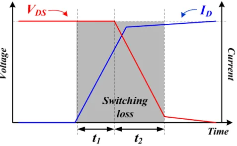
2.1.1 Losses and Efficiency
2.1.1.1 Conduction Loss
Power loss of regulators is the combination of the switching loss and the MOSFET’s conduction loss in Eq. (1). The conduction loss also can classify into high-side transistor loss and low-side transistor loss.
MOSFET SW COND
P P P (1)
Calculating the high-side conduction loss is straightforward that the conduction loss is just the I2R loss timing the MOSFET’s duty cycle as below:
2 ( ) OUT COND OUT DS ON IN V P I R V (2)
Where RDS(ON) is at the maximum operation MOSFET junction temperature (TJ(MAX))
Low-side loss are also comprised of conduction loss and switching loss. Conduction loss for low-side is given by:
2 ( ) (1 OUT) COND OUT DS ON IN V P I R V (3)
2.1.1.2 Switching Loss
The switching interval begins when the high-side MOSFET driver turns on and begins to supply current power MOSFET’s gate to charge its input capacitance. There is no switching loss until VGS reaches the MOSFET’s VTH therefore power loss equal zero.
13
Fig. 6. Transient waveform of VDS and ID curve in switching losses.
When VGS reaches VTH, the input capacitance (CISS) is being charged and ID (the
MOSFET’s drain current) is rising linearly until it reaches the current IL which is presumed
to be Iout. During this period (t1) the MOSFET is sustaining the entire input voltage across it,
the energy in MOSFET during t1 is:
1 1 ( 2 )
in out t
V I
P t (4)
Now, we enter t2. At this point, Iout is flowing through high-side MOSFET, and the VDS
begin to fall. All of the gate current will be going to recharge CGD. CGD is similar to the
“Miller” capacitance of transistor, so t2 could be thought of as “Miller time”. During this
time the current is constant (at Iout) and the voltage is falling fairly linearly from VIN to 0,
therefore: 2 2 ( 2 ) in out t V I P t (5)
The switching loss for any given edge is just the power that occurs in each switching interval, multiplied by the duty cycle of the switching interval:
1 2 ( ) ( ) 2 in out SW S V I P t t F (6)
14
2.1.1.3 Static Loss
The static loss also called as quiescent loss that was consumed by controllers of switching regulators. The smaller quiescent loss had higher efficiency.
Q in Q
P V I (7)
The other power losses that don’t be mentioned above obeyed the rules of I2R.
2.1.1.4 Efficiency
The efficiency of switching regulator is defined as the ratio of the output power consumption and input power supplies, formed as below:
100% O O ff in O Q SW COND Else P P E P P P P P P (8)
The input power supplies consist of the output consumption (PO), quiescent loss (PQ),
switching loss (PSW), conduction loss (PCOND) and other losses (PElse) in parasitic elements.
A high efficiency results in a high performance extending the battery life.
2.1.2 Load and Line Regulation
Switching regulators are powerful system of stepping up or down the desires voltage. Therefore, to keep the regulated voltage and decrease the steady state error when increasing the supply voltage and load condition of DC-DC converter is most important.
The load regulation is defined as the percentage of steady state error of output voltage when the load condition changes and can be calculated as follows.
15
_
100
%
.
out
out norm load
V
Load Regulation
V
I
mA
(9)The line regulation is defined as the percentage of steady state error of output voltage when the input voltage changes and can be calculated as follows.
_
100
%
.
out out norm INV
Line Regulation
V
V
mV
(10)2.1.3 Transient Response
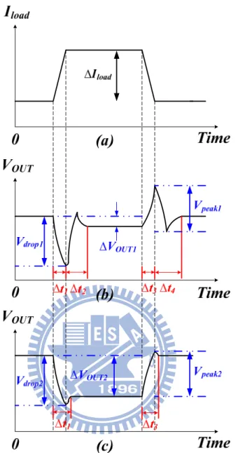
The transient response is an important specification of DC-DC converter for the system applications [10]. The large load current changes suddenly will cause a voltage fluctuation at output of DC-DC converter. The voltage fluctuation may trigger the logic circuit or affect the analog circuit. Therefore, it’s important to reduce the large voltage changing and the time during voltage variation. The transient response of output voltage relates to load current is shown in Fig. 7. During the first period Δt1, the large current flow into the output
load from DC-DC converter, due to the DC-DC converter cannot provide enough energy to maintain the output voltage, the output voltage will drop in this period because the output capacitor discharges the energy to support the load current. The drop voltage is shown in Eq. (11). According to the parameters of Eq. (11), selecting the output capacitor well can reduce the drop in this period.
16
Fig. 7. The transient response of output voltage relates to load current.
1
1 2
drop drop out ESR out
t
V
V
I
R
C
(11)During the second period Δt2, the system senses the output variation by feedback
loop then turn on the power P-type MOSFET to recover the regulated output voltage. The sum of Δt1 and Δt2 is called the recovery time and the second periodΔt2 depends on the
system bandwidth of the DC-DC converter
The static error ΔVOUT between light load and heavy load is relates to the voltage
17
to the Fig. 7(b) and Fig. 6(c), the performance of Fig. 7(b) due to the large DC gain and causes the better load regulation, but the second period Δt2 extend the recovery time.
However, it reduces the time of transient response. The performances of Fig. 7(c) due to the poor DC gain and cause huge static error but reduce the time of second period Δt2 and
improve the dynamic performance.
When the load current is decreasing to light load suddenly, the output voltage will jump until the DC-DC converter start to recovery the regulated voltage. The redundant current charges the output capacitor resulting to a peak voltage as shown in shown in Eq. (12) before the feedback loop of DC-DC converter react.
3
1 2
peak peak out ESR out
t
V
V
I
R
C
(12)During the final periodΔt4 the output capacitor discharged the redundant current to
feedback resistors. As mention described, the transient response is relates to the bandwidth of DC-DC converter, output capacitor, equivalent series resistance (RESR) of output voltage
18
2.2 Modulation
Technologies
There are two mainly kind of modulation technologies in switching regulators. Firstly, PWM modulates the switching signal by a fixed switching frequency. Secondly, PFM uses a hysteresis window to generate a switching signal. Both of the technologies modulate the on and off time of switches to control the energy transfer to output.
2.2.1 Pulse Width Modulation (PWM)
Operating with PWM control, the power MOSFET are controlled by a constant clock cycle, the PWM control waveform is shown in Fig. 8 [12] [13]. While the ramp signal is lower than the control signal, the PWM signal at high level; the ramp signal is higher than the control signal, the PWM signal changes to low level. The main modulation is change the width of every clock cycle by the control signal and the output voltage is determined by the duty ratio of the PWM signal.
Fig. 8. Pulse width modulation waveform.
19
total power loss is expressed as follows.
2
(
)
2SW CON OUT Duty GP GN IN SW
P
P
I
R
C
C
V
F
(13)As shown in Eq. 13, operating at PWM control the switching frequency is constant but output current varies with loading. That is to say, the switching loss is invariable with load but conduction loss will increase with the output loading, as shown in Fig. 9.
Fig. 9. Analysis of conduction loss and switching loss at pulse width modulation.
2.2.2 Pulse Frequency Modulation (PFM)
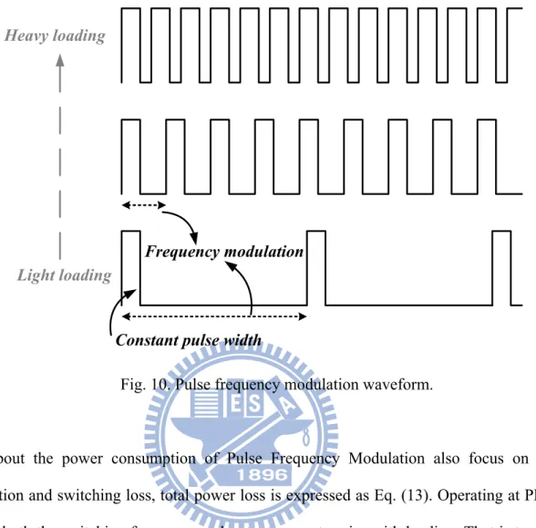
Operating with PWM control, the power MOSFET are controlled by a vary frequency, the PFM control waveform is shown in Fig. 10 [14] [15]. The on-time of PFM controller is constant width and off-time is variable with loading. By controlling the off-time of every switching cycle can obtain different switching signal to achieve desirable output voltage. Therefore, the smaller output loading can reduce the switching frequency.
20
Constant pulse width Frequency modulation
Light loading Heavy loading
Fig. 10. Pulse frequency modulation waveform.
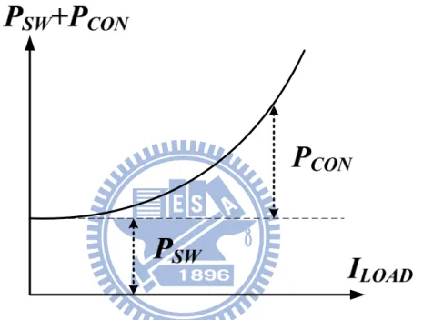
About the power consumption of Pulse Frequency Modulation also focus on the conduction and switching loss, total power loss is expressed as Eq. (13). Operating at PFM control both the switching frequency and output current varies with loading. That is to say, the switching loss and conduction loss will increase with the output loading, as shown in Fig. 11.
21
Fig. 11. Analysis of conduction loss and switching loss at pulse frequency modulation.
2.3 Descriptions of Ripple-Based Control
Methods
Three kinds of ripple-based control method of buck converter including hysteretic control, constant on-time control and constant off-time control are introduced in this section.
2.3.1 Hysteretic Control Method
The hysteretic controller is shown in Fig. 12 [16], the main control method is generating a hysteresis window. By controlling the upper and lower boundary to regulate the output voltage, when the feedback voltage touch to the hysteretic upper boundary, the power N-type MOSFET will turn on and power P-type MOSFET will turn off to discharge the inductor current and feedback voltage will decrease. At the same time, the hysteretic
22
window will change to the lower boundary. While the feedback voltage touch to the hysteretic lower boundary, the power P-type MOSFET will turn on and the power N-type MOSFET will turn off to charge the inductor current and feedback voltage will increase. The hysteretic window which is calculating by superposition theorem can be expressed as follows.
2 1 2 1
1 2 1 2 1 2 1 2
(
) (
)
H uppper lower REF IN REF IN
R
R
R
R
V
V
V
V
V
V
V
R
R
R
R
R
R
R
R
(14)The features of hysteretic controller are described as follows; firstly, the main control circuit is comparator and the error amplifier does not be used, so it is no problem about system compensation. Secondly, without using any clock generator, the switching frequency of hysteretic controller is generated by system itself. The following is the calculation of feedback voltage variation, as expressed as follows.
0
0
(1
)
FBAVG FB OFF FBAVG IN
FB OFF
dV
V
V
t
V
DV
D T
I
C
C
V
dt
R
t
RC
RC
(15)The voltage VFBAVG is the average voltage of feedback voltage, ideally is DVIN, the
parameter D is the duty ratio of buck converter. And the hysteresis window variation (VH)
equals to feedback voltage variation (ΔVFB). Combining the Eq. (14) and Eq. (15), the
switching frequency can as expressed as follows.
1 0 2 0 1 2 0 1
(1
)
1
1
(1
)(1
)
IN H FB INR
DV
D T
R
V
V
V
f
D
D
R
R
RC
T
RC
R
(16)By controlling the resistor R, capacitor C and the ratio of resistors R1 and R2 can define
the switching frequency. However, as line and load conditions change, the hysteretic regulator operates over a wide frequency range that depends on the input and output voltages, the output filter inductance, the hysteresis window and ESR of output capacitor. Finally, because the output ripple has been defined, it can’t choose the low ESR capacitor to
23
reduce output ripple.
V
REFR
1 Gate DriverM
NM
PV
INV
OUTR
C
L
R
LR
esrC
oC
TR
T LoadR
2 Deadtime CompV
FBFig. 12. The block diagram of hysteretic control method.
2.3.2 Constant On-time Control Method
As shown in Fig. 13, the basic constant on-time control structure consists of a comparator and one-shot on-time timer, with the output voltage feedback compared with an internal reference. The constant on-time control method is a modification of hysteretic control that operates at a relative constant frequency without an oscillator. It controls the high side power MOSFET switch whose on-time varies inversely with the input supply voltage.
In normal operation, the system initiates an on-time period when the feedback voltage VFB falls below the reference voltage VREF, which can be viewed as a valley voltage. The
high side power P-type MOSFET stays on for the programmed on-time, causing the feedback voltage to rise above the reference voltage. After the on-time period, the power
24
P-type MOSFET remains off until the feedback voltage falls below the reference voltage. Besides, the one-shot on-time timer provides a period that is inversely proportional to input supply voltage for constant frequency operation over input supply voltage variation.
Fig. 13. The block diagram of constant on-time control method.
In continuous conduction mode (CCM) the frequency depends only on duty cycle and on-time period. This is in contrast to hysteretic regulators where the switching frequency is determined by the output inductor and capacitor. In discontinuous conduction mode (DCM), experienced at light loads, the frequency will vary according to the load condition, similar to the operation in PFM mode [17]. This leads to high efficiency and good transient response.
25
Fig. 14. Inductor current and feedback voltage waveforms in DCM operation of constant on-time control.
Fig. 14 shows the waveforms of constant on-time control in DCM operation, inductor current IL raises to peak value during the fixed on-time period, and it falls back to zero
before feedback voltage VFB reaches valley voltage VREF for constant on-time control.
When VFB reaches VREF, the next on-time period is introduced. Therefore, the off-time
period of constant on-time control is dependent on load current condition in DCM operation.
2.3.3 Constant Off-time Control Method
The approach of constant off-time control is similar to constant on-time control. In normal operation, the system initiates an off-time period when the feedback voltage VFB
rises above the reference voltage VREF, which can be viewed as a peak voltage. However,
26
power management system. The reason is that the switching frequency in DCM operation of constant off-time control is inversely proportional to the load current.
Fig. 15. Inductor current and feedback voltage waveforms in DCM operation of constant off-time control.
As shown in Fig. 15, the off-time period of constant off-time control is fixed, which is independent of load current condition. However, the voltage difference ΔV is proportional to output current. As the ΔV becomes larger, the VFB needs to extend on-time period to
reach VREF to cause the decrease of the switching frequency. The switching frequency
increases as output current decreases in the DCM. It deteriorates the system efficiency. Thus, constant on-time control is widely used in practice [18].
27
Chapter 3
Topology of Constant On-time
Control DC-DC Buck Converter
without ESR Compensation
In this chapter, the system stability analysis and operation of proposed constant on-time control DC-DC buck converter are presented. The system stability analysis of conventional constant on-time control converter is shown in section 3.1. In section 3.2, the system operation is introduced.
3.1
System Stability Analysis of Conventional
Constant On-time Control
The basic concept of constant on-time control is introduced in chapter 2. Besides, constant on-time control is more popular than constant off-time control owing to the conversion efficiency at light loads. In this section, we will analyze the system stability of constant on-time control in time-domain and frequency-domain, respectively.
28
Fig. 16. Small ESR caused double-pulse problem.
In conventional constant on-time control with small ESR value on the output capacitor, the converter is easily affected by the noise due to small output ripple, which is dominated by the ripple on the output capacitor. Besides, the loop phase delay may further decrease the system stability owing to the double-pulse problem. As illustrated in Fig. 16, the delayed output voltage, Vout, is unable to reach the reference voltage, Vref, even after the first
constant on-time period. Consequently, the second constant on-time is inserted after the minimum off-time period to raise Vout higher than Vref. The constant on-time control can’t
regulate the output voltage within one switching cycle and thus induces the double-pulse problem. That is, the system needs two or more switching periods to regulate the output voltage. The output voltage ripple is increased to ensure the system stability due to the decreased switching frequency.
In Fig. 16, the slope of the inductor current is m, which is expressed in Eq. (17), during the on-time period.
29 in out L
V
V
dI
m
dt
L
(17)The value of Vout for time=t can be calculated as shown in Eq. (18). Resr is the ESR on
output capacitor, CO. Lesl is the ESL on the output capacitor. ΔIL is the inductor current
variation during one on-time period.
1
( )
(
)
Lout ref esr L esl O
dI
V
t
V
R mt
I
mt dt
L
C
dt
(18)The output ripple is composed of three components including ESR part, capacitor part and ESL part. In Eq. (18), the second term indicates the contribution of the ESR while the third term represents the ripple on the output capacitor. The last term indicates the contribution of the ESL. To ensure the system can be regulated for each switching cycle. At t=TON, the value of Vout(TON) needs to be larger than Vref as shown in Eq. (19).
2 2
(
)
0
2
ON ONout ON ref esr ON esl O O
mT
mT
V
T
V
R mT
L m
C
C
(19)The arrangement of Eq. (19) can be expressed in Eq. (20).
2
esl O ON esr O ONL C
T
R C
T
(20)Generally speaking, as the ESL of output capacitor is not sufficient large, the criterion of system stability is decided by the time constant, ResrCO, and it can be derived in Eq. (21).
2
ON esr O
T
R C
(21)30
the system stability. Consequently, the ripple contributed by the ESR dominates the whole output ripple to guarantee the system stability. Therefore, a large ESR is utilized in the conventional constant on-time control at the sacrifice of large output ripple. However, for certain applications of output capacitor combination, as the total ESL of the output capacitor becomes larger, the double-pulse problem will appear as shown in Fig. 17. At the beginning of the minimum off-time, the voltage across ESL will step down since the negative slope of inductor current. If the voltage spike on the ESL is larger enough to let the output voltage smaller than Vref, the second constant on-time period will appear. Large ESL will cause the
system unstable due to large step voltage on ESL.
Fig. 17. Large ESL caused double-pulse problem.
Considering the noise causes the variation of reference voltage as shown in Fig. 18, the rising edge of the power MOSFET switching signal is perturbed to induce a large jitter. The time deviation of tn indicates the jitter caused by the noise. Unfortunately, the switching
frequency can’t be kept constant and thus the system suffers from the electromagnetic interference (EMI) problem. The performance of system is seriously deteriorated. Thus,
31
small jitter and constant switching frequency are also demanded in the constant on-time control.
Fig. 18. The noise effect on feedback voltage and power MOSFET switching signal. Fig. 19 shows the enlarged waveform of Vfb with a negative slope of a when the
inductor current decreases. If the slope becomes more sharp and has a value of a’, the new waveform of Vfb’ decides another switching period. Once the noise perturbs the reference
voltage from Vref to Vref’, the variation of switching period can be decreased from t1 to t0
due to the sharp slope. Basically, the slope can be expressed as Eq. (22), which is proportional to the value ESR. Eq. (22) is under the assumption of neglecting the voltage across ESL and capacitor. In other words, the ESR value can determine the system stability in the constant on-time control. Thus, the conventional design uses a large ESR value to suppress the jitter problem. A lower jitter effect can be derived by a larger ESR value. But, a large ESR value will cause the increase of output ripple and transient dip voltage.
2 1 2
esr out FB esr
FB FB
R
V
R
R
slope
L
R
R
L
(22)32
Fig. 19. Enlarged waveform of feedback voltage and reference voltage that affected by noise.
A large ESR is usually selected to avoid the double-pulse problem. In other words, the ripple content at the output voltage should have a minimum value to maintain the system noise margin. The larger ESR value causes the larger output voltage ripple. For the purpose of solving the dependence of ESR value, the proposed constant on-time control DC-DC converter provides sufficient noise margin without using large ESR capacitor so that the low jittery behavior can be attained to eliminate the double-pulse problem.
33
3.2
Topology of the Proposed System
Fig. 20. Topology of proposed constant on-time control DC-DC buck converter.
Fig. 20 shows the proposed constant on-time control DC-DC converter without ESR compensation. The Vout is regulated by the loop comparator through the voltage divider,
RFB1 and RFB2. The Vr from the zero ESR compensation circuit and the feedback voltage Vfb
are compared by the loop comparator. The output of loop comparator is used to decide the timing to store energy in the inductor. The minimum off-time signal Voff is used to provide a
minimum off-time period to ensure a minimum off-time during startup interval and extreme duty condition. Besides, the zero current detector signal, Vzcd, is used to avoid the reverse
inductor current. The deadtime control circuit is used to avoid the short-through current. The output stage of converter can be viewed as an integrator. As a result, the output voltage ripple can be recognized as an integration of the inductor current ripple. Therefore, the inductor current information can be derived by differentiating the output voltage. As shown in Fig. 21, the proposed zero ESR compensation technique generates a differential
34
signal Vs to get the inductor current information. Vs can be viewed as a ramp signal,
providing good noise immunity for system operation [19]. However, the ESL, Lesl, on
output capacitor CO will distort the differential signal of the conventional differentiator. The
output voltage Vout contains high frequency component caused by Lesl. It will deteriorate the
system stability due to the double-pulse problem. Afterwards, the Vs goes through the
reflector, which produces the reflective signal Vr. Once the inductor current rises up, Vr
starts to fall. Fortunately, the Vr can generate a sufficient noise margin at the input node of
loop comparator.
Output voltage ripple
V
outDifferentiator
V
sv
outDifferential signal
V
rReflective signal
Reflector
Zero ESR
Compensation
equivalent series inductor effect
v
sv
rcrooked curve due to small ESR
small ESR effect
off-time period on-time period
35
V
fbI
L
V
r
Enlarged noise marginV
s
V
SWP
time (s)
On-time period Reflecting Sensingtime (s)
time (s)
time (s)
Switching periodFig. 22. The operational scheme of the proposed technique.
At the beginning of the inductor charging period, the control signal Vclr clears the
on-time timer in order to recount on-time period. As on-time period ends up, the signal Vreset
goes from low to logic high. The high-side power MOSFET SWP turns off to start the
inductor discharging period to release the stored energy. When the Vr rises above the Vfb,
the high-side power MOSFET SWP turns on and the on-time timer is cleared, again, to
restart the inductor charging period as shown in Fig. 22. The Vfb is compared with the Vr,
which represents the opposite shape of the differential signal Vs. The ripple of Vfb is much
smaller than Vr. That is, Vr can be regard as the feedback voltage in the original constant
on-time control and the Vfb can be regard as the reference voltage. In other words, the Vfb
can be viewed as the peak voltage of the Vr. When the Vr starts to decline from the level of
Vfb, the slope of Vr is sufficient steep and thus it can provide good noise immunity. That is,
36
Chapter 4
Circuit Implementation
In this chapter, the sub-circuits of the proposed constant on-time control DC-DC buck converter are introduced. In section 4.1, zero ESR compensation circuit is presented. It consists of differential circuit part and reflection circuit part. In section 4.2, the on-time timer is presented. It generates one on-time pulse each switching cycle to control switches.
4.1 Zero
ESR
Compensation
Circuit
The proposed zero ESR compensation circuit is depicted in Fig. 23. The differentiator is composed of M1-M9, C1-C2, and OP1. Differentiating feedback voltage Vfb through the
capacitor C1, the inductor current can be derived. Vd is composed of ESR and inductor
current ripple information. However, Vd has unwilling distortion due to equivalent series
inductor effect of output capacitor. The expressions of Vfb and Vd are shown in Eq. (23) and
Eq. (24), respectively.
1
L fb esr L L esl Odi
V
k R i
i dt
L
C
dt
(23) 2 ' 2 in out L L d fb esr esl OV
V
i
d i
V
V
k R
L
L
C
dt
(24)k is the feedback ratio and τ is a constant generated in the procedure of differentiation. The unwilling ESL effect caused by Lesl is a high frequency component, which will result in
37
the gates of transistors M6 and M7. Therefore, the current IL flowing into M7 is filtered by
C2. That is, the high frequency component of Vd has been eliminated. Then, the equivalent
series inductor effect can be reduced. After that, the current IH flowing into M8 is mirrored
to M9, and IH is the deduction of IHL about IL. That is, IH contains high frequency
component of Vd. The low frequency component current IL can be obtained by deducting IH
from IHL. The voltage Vs would therefore contain low frequency component only,
eliminating the equivalent series inductor effect of output capacitor. The expression of Vs is
shown in Eq. (25).
Fig. 23. The proposed zero ESR compensation circuit.
in out L s esr O
V
V
i
V
k R
L
C
(25)38
operational amplifiers OP2 and OP3, constitute the voltage-to-current converter. R1, R2 and
R3 are the conversion factors of the voltage-to-current converter. The Vref decides the DC
level of the Vr, which affects the DC level of the Vout. The expression of Vr is shown in Eq.
(26). 3 1 2
(
ref s)
rV
V
V
R
R
R
(26)4.2 On-Time
Timer
Fig. 24. The on-time timer.
Fig. 24 shows the on-time timer circuit. The transistors M1-M4 and the resistor Ron
generate a current Ion to charge the capacitor Con. Variable current Ion depends on the Vin. Ion
39 1 in GS on on
V
V
I
R
(27)The transistors M5-M6 and Vclr are used to decide the on-time capacitor, Con, to be
charged or discharged. At the beginning of first switching period, Vclr is high and Con is
charged by Ion. Then, Von is raised. As the Von reaches the Vout, the Vreset becomes high to
decide the on time period. As a result, the time Ton required to reach Vout is inversely
proportional to the Vin and proportional to the Vout. Ton is expressed in Eq. (28).
1 on out on out on on on in GS
C V
C V R
T
I
V
V
(28)The switching frequency is relatively constant as the duty ratio D as expressed in Eq. (29). out in
V
D
V
(29)4.3
Control Logic Circuit and Flow Chart
Fig. 25 shows the detailed control logic circuit of the proposed constant on-time control DC-DC converter. The circuit consists of one inverter, two AND gates, two OR gates and two SR-latch. The purpose of the control logic circuit is producing the pulse width modulation (PWM) switching signal VSWP and VSWN to control power MOSFET SWP and
SWN. Voff and Vzcd are the minimum off-time timer signal and zero current detector signal,
respectively. Voff, when the minimum off-time period gets through, it will go from logic low
to logic high. Vzcd, goes from logic low to logic high as the reverse inductor current appears,
40
feedback voltage and reflective voltage of differential signal Vs. Vreset, produced by on-time
timer, resets the SR-latch in order to turn off the power MOSFET SWP.
Fig. 25. The control logic circuit.
Fig. 26 shows the flow chart of control logic circuit, it can be divided into two parts, on-time period and off-time period. The logic level of inner nodes in the control logic circuit is shown in the flow chart, which interprets the operational procedure of proposed converter.
41
42
Chapter 5
System of Reduction of Equivalent
Series Inductor Effect in Constant
On-Time Control DC-DC Converter
without ESR Compensation Simulation
Results, Conclusions and Future Work
In this chapter, the simulation results are shown in section 5.1. The conclusions are made in section 5.2. Finally, the future work is shown in section 5.3.
5.1 Simulation
Results
The circuit was fabricated in TSMC 0.25µm CMOS process. The chip layout is shown in Fig. 27 The filter components contain L=4.7µH, CO=4.7µF, Resr=0mΩ and Lesl=2nH. The
input voltage ranges from 3V to 4.5V and output voltage is 2V. The switching frequency is designed as 1MHz.
43
Fig. 27. Chip layout.
Fig. 28 shows the output waveforms at different load current condition when the converter operates in the CCM and DCM. Fig. 28(a) and (b) show that the proposed zero ESR compensation technique adjusts the switching frequency of the buck converter
dynamically according to the load current condition. When the load current is about 30mA, the switching frequency is about 377kHz. As the load current increases to 50mA, the switching frequency increases to 660kHz. On the other words, when the converter operates in the DCM, the switching frequency is proportional to the load current condition. Besides, the noise margin between Vfb and Vr is not less than 80mV. Fig. 28(c) shows the converter
correctly operates in the CCM without the double-pulse problem when 2nH of ESL and no ESR exist at output capacitor. The output voltage ripple is about 2.6mV due to small ESR.
44
Furthermore, the switching frequency reduces for power saving when the load current decrease in the DCM.
(a)
45
(c)
Fig. 28. Waveforms of the output voltage and inductor current at different load current condition. (a) Iload =30mA (b) Iload =50mA (c) Iload =100mA.
As shown in Fig. 29, simulation results of the output voltage and the inductor current demonstrate the CCM operation during load transient response. The recovery times are about 9µs and 10µs when the load current changes from 100mA to 600mA and vice versa, respectively, if Vin = 3.3V. The zero compensation circuit provides good noise margin for
constant on-time control system to operate correctly with no ESR exist at output capacitor. Besides, constant on-time control can achieve fast transient response since the system is not need frequency compensation. The specifications are listed in Table II.
46
(a)
(b)
Fig. 29. Transient response (a) when load current changes from 100mA to 600mA and (b) from 600mA to 100mA.
47
5.2 Conclusions
A reduction of equivalent series inductor effect in constant on-time control DC-DC converter without using ESR compensation is proposed to eliminate equivalent series inductor effect of output capacitor and remove the dependency of output ripple induced by ESR. Besides, the noise margin at the comparator input node has been increased.
Furthermore, although the ramp compensation is applied at feedback point, the system still presents a good transient response. The system can operate correctly even that no ESR exists at output capacitor both in CCM and DCM.
TABLE II. DESIGN SPECIFICATIONS.
PARAMETER VALUE UNIT
Supply variation (Vin) 3 - 4.5 V
Output voltage (Vout) 2 V
Switching frequency 1 MHz Undershoot voltage recovery time
@ IOUT changesfrom 100mA to 600mA
9 μs Overshoot voltage recovery time
@ IOUT changes from 600mA to 100mA
10 μs Maximum load current 800mA mA
Inductor (L) 4.7 μH Output capacitor (Co) 4.7 μF
ESR on output capacitor (Resr) 0 Ω
48
5.3 Future
Work
The proposed zero ESR compensation technique not only removes the need of conventional ESR compensation but also aims to eliminate ESL effect of the output capacitor. Besides, fast transient response and small dip voltage variation can be achieved. The noise margin at the loop comparator input nodes can also be extended. Therefore, the SNR of the constant on-time control system is increased. However, the phase delay caused by zero ESR compensation circuit will reduce the noise margin and deteriorate the transient response. In addition, the output voltage DC level is not accurately defined. On the other words, the output voltage accuracy will be affected by parasitic component, such as ESR and ESL. Finally, the experimental result should be presented to prove simulation result of whole system is matching.