國 立 交 通 大 學
電子工程學系 電子研究所
博 士 論 文
低溫複晶矽薄膜電晶體之氟鈍化製程與可靠度的
研究
Study on Fluorine Passivation Techniques and the
Reliability for Low Temperature Polycrystalline
Silicon Thin-Film Transistors
研 究 生 :王 獻 德
指導教授 :雷 添 福
低溫複晶矽薄膜電晶體之氟鈍化製程與可靠度的研究
Study on Fluorine Passivation Techniques and the
Reliability for Low Temperature Polycrystalline Silicon
Thin-Film Transistors
研究生:王獻德 Student:Shen-De Wang
指導教授:雷添福 博士
Advisor:Dr. Tan-Fu Lei
國立交通大學
電子工程學系 電子研究所
A Dissertation
Submitted to Department of Electronics Engineering
and Institute of Electronics
College of Electrical Engineering and Computer Science
National Chiao Tung University
In Partial Fulfillment of the Requirements
For the Degree of
Doctor of Philosophy
in
Electronics Engineering
September 2005
Hsinchu, Taiwan, Republic of China
低溫複晶矽薄膜電晶體之氟鈍化製程與可靠度
的研究
學生: 王 獻 德
指導教授: 雷 添 福 博士
國立交通大學
電子工程學系 電子研究所博士班
摘 要
此論文提出多種氟鈍化(passivatation)技術以製作高效能且高可靠度的複晶 矽薄膜電晶體(poly-Si TFTs)。此外,我們亦研究在電壓應力(electrical stress)測試 下,複晶矽薄膜電晶體之開啟電流(On-current)及關閉電流(Off-current)的不穩定 性 。 最 後 , 我 們 利 用 高 解 析 度 的 掃 描 式 電 容 顯 微 鏡(scanning capacitance microscopy, SCM)系統開發出一種探測氧化層崩潰(oxide breakdown)點的技術。首先,我們提出與現有製程具高度匹配性的四氟化碳電漿處理(CF4 plasma
treatment)技術,用以製作高效能的固態結晶(solid-phase-crystallized)之複晶矽薄 膜電晶體。利用此技術,氟原子可以有效地被導入複晶矽薄膜中以消除薄膜中的 載子補獲態(trap states),進而有效地提升元件特性。經由四氟化碳電漿處理的複 晶矽薄膜電晶體具有好的臨限擺幅(subthreshold swing)、低的臨界電壓(threshold voltage) 及 高 的 元 件 開 關 電 流 比 (On/Off current ratio) ; 其 載 子 電 致 遷 移 率 (field-effect mobility)也提升了 22.8 %。此外,四氟化碳電漿處理也提升元件的抗 熱載子(hot-carrier)破壞的能力。之後,我們在將此技術搭配準分子雷射退火 (exciner laser annealing),應用於製作高性能的雷射處理之複晶矽薄膜電晶體
(ELA poly-Si TFTs)。實驗結果證明氟電漿處理能有效地鈍化複晶矽中及氧化層與 複晶矽界面上的缺陷。因此,元件的特性可獲得大幅的提升。最重要的是因為矽 -氟的高強度鍵結能,經過熱載子應力(hot carrier stress)測試後,發現摻入氟原子 的複晶矽薄膜電晶體具有較好的可靠度。另外,我們亦提出一種利用氟矽玻璃 (fluorinated silicate oxide, FSG)當緩衝層的複晶矽薄膜電晶體製程。利用此方法亦 可有效的鈍化複晶矽缺陷,進而大幅改善元件特性、均勻性及可靠度。其中,氟 在氟矽玻璃中最佳的含量大約介於 2% 到 4% 間。
接著,本論文探討複晶矽薄膜電晶體在不同電壓應力測試下的開啟電流 (On-current)及關閉電流(Off-current)的不穩定性。利用施加不同的閘極及汲極電 壓來研究應力測試下所產生的元件劣化情形。經由結果我們歸納出,氧化層的捕 獲電荷(trap charges)及複晶矽通道中的載子補獲態(trap states)之數量與空間分佈 是造成開啟電流(On-current)及關閉電流(Off-current)的變化的最主要因素。我們 利用此技術完成一個完整的模型以解釋複晶矽薄膜電晶體的開啟電流及關閉電 流之不穩定性的原因。
在論文的最後,我們開發出一種利用掃描式電容顯微鏡(scanning capacitance microscopy, SCM)搭配原子力顯微鏡(atomic force microscopy, AFM)的探針掃描 技術以研究氧化層的崩潰(oxide breakdown)現象。此技術可以清楚地掃描出氧化 層 崩 潰 點(breakdown spots) 的 局 部 分 佈 。 這 些 崩 潰 點 因 為 具 高 度 導 通 性 (conductivity)因而顯示出非常低的微分電容值(dC/dV)訊號。由結果顯示出,氧化 層的崩潰點的直徑大概為 6 奈米(nm)到 13.5 奈米之間。此外,根據原子力顯微 鏡的結果,我們亦發現氧化層的崩潰現象並不會造成其表面平坦度的改變。
Study on Fluorine Passivation Techniques and the
Reliability for Low Temperature Polycrystalline
Silicon Thin-Film Transistors
Student: Shen-De Wang
Advisor: Dr. Tan-Fu Lei
Department of Electronics Engineering &
Institute of Electronics
National Chiao Tung University
ABSTRACT
In this thesis, various fluorine passivation techniques for fabricating high-performance and high-reliability polycrystalline silicon thin-film transistors (poly-Si TFTs) are proposed and discussed. In addition, the On-current (Ion) and
Off-current (Ioff) instabilities of poly-Si TFTs under electrical stress are thoroughly
investigated. At last, a new scheme by employing high-resolution scanning capacitance microscopy (SCM) is developed to scan the breakdown spots on oxide films.
First, a process-compatible CF4 plasma treatment for fabricating
high-performance solid-phase-crystallized (SPC) poly-Si TFTs is demonstrated. Using this technique, fluorine atoms can be introduced into poly-Si films to passivate trap states, and hence the performance of SPC poly-Si TFTs can be significantly improved. The fluorinated SPC poly-Si TFTs exhibit good subthreshold slope, low threshold voltage, and better On/Off current ratio. The fluorinated poly-Si TFT also shows approximately 22.8 % enhancement in the maximum field-effect mobility. Moreover,
the CF4 plasma treatment also promotes the device’s hot-carrier immunity. Then, CF4
plasma treatment combined with excimer laser annealing (ELA) is proposed to fabricate high-performance ELA poly-Si TFTs. Fluorine can effectively passivate the trap states near the SiO2/poly-Si interface. With fluorine incorporation, the electrical
characteristics of ELA poly-Si TFTs are significantly improved. The CF4 plasma
treatmentalso improves the device reliability of ELA poly-Si TFTs with respect to hot-carrier stress, which is due to the formation of strong Si-F bonds. Another fluorine passivation technique is also proposed by adopting fluorinated silicate oxide (FSG) as a buffer layer. Experimental results reveal that the device performance, uniformity and reliability can be remarkably improved with appropriate fluorine content (2% to 4%) in the FSG layer.
Then, the On-current (Ion) and Off-current (Ioff) instabilities of poly-Si TFTs are
thoroughly investigated under various electrical stress conditions. The stress-induced device degradation is studied by measuring the dependences of Ion and Ioff on the
applied drain/gate voltages. From the results, dissimilar variations of Ion and Ioff can be
observed, which is attributed to the variances in the amount of trap charges in the gate oxide and the spatial distributions of trap states generated in the poly-Si channel. A comprehensive model for the degradation of Ion and Ioff in poly-Si TFTs under various
electrical stress conditions is proposed.
Finally, scanning capacitance microscopy (SCM), combined with atomic force microscopy (AFM), is employed to investigate the dielectric breakdown phenomena in SiO2 films. The localized breakdown spots can be clearly imaged by this technique.
The breakdown spots exhibit signals with low differential capacitance (dC/dV) due to high conductivity. The diameters of these breakdown spots are from 6 nm to 13.5 nm. Moreover, according to the corresponding AFM images, theirsurface morphology shows little change after the occurrence of oxide breakdown.
誌謝
首先我要向我的指導教授雷添福博士致上最高的敬意。感謝他在學業研究與 生活上給我的指導與鼓勵。在這四年的學習生涯中,讓我學習到研究的態度及方 法,也讓我能充實自我的學問。此外,我也要感謝趙天生教授、簡昭欣教授、崔 秉鉞教授、張茂男博士與林孝義博士無論是在課堂上、研究上或平日會議時給我 的非常多地指導與幫助,令我獲益良多。 感謝張子云學長帶我進入半導體領域,還有李名鎮、俞正明、李介文、陳志 遠學長對我的照顧及協助。特別要感謝我所帶過的兩位學弟羅韋翔與桑任逸,此 論文是我們一齊努力出來的成果。此外,已畢業的溫凰君、陳筱薇學姊及李美錡、 謝德慶同學,謝謝你們陪我度過漫長的實驗時間。也感謝實驗室裡一起研究的夥 伴,謝明山、小強、建豪、楊紹明、小賢、伯儀、志仰、家文,以及久盟、松霖、 國誠、余俊、伯浩、宗元、梓翔、源俊、俊嘉、統億、錦石、子恆、張婷以及李 耀仁、林家彬學長,有你們的陪伴與討論,實驗過程不再枯燥乏味而是充滿著歡 樂。因為有你們的幫忙與笑聲,讓我能以快樂的心情面對實驗上與生活上的挑戰。 由衷地感激在實驗中曾給我幫助的朋友們,特別是計測實驗室的彭作煌先 生、教學實驗室的彭兆光先生,與奈米中心的徐秀鑾、林素珠、黃月美、楊月嬌、 范秀蘭、陳悅婷、何惟梅、劉曉玲小姐以及奈米元件實驗室徐台鳳小姐及其他工 程師們,若沒有你們的大力幫忙,我無法順利地完成此論文,在此獻上我最深的 敬意。 最後,謝謝我的家人與我可愛的女友,感謝你們在我心情低落時給我打氣, 在我需要溫暖時給我照顧,謝謝你們陪我一路走過這漫長的求學生涯。僅此論文 獻給所有關心我的朋友。Contents
Abstract (Chinese) ………I
Abstract (English) ………..III
Acknowledge ………V
Contents ………..VI
Figure Captions& Table Lists .………..………... IX
Chapter 1 Introduction ……….1
1.1 Overview of Poly-Si Thin-Film Transistors ....………...1
1.2 Motivation ……….………..……...3
1.3 Thesis Organization ……….………..5
References ………8
Chapter 2 CF4 Plasma Treatment on Solid-Phase-Crystallized (SPC) Poly-Si TFTs.………....…....……….………...16
2.1 Introduction ……….………...…..16
2.2 Experimental …...………..………...………..17
2.3 Results and discussion………..18
2.3.1 Comparison of Device Characteristics ....………...……..…..18
2.3.2Extraction ofTrap StateDensity..………..……..19
2.3.3 OutputCharacteristicsandActivationEnergy...….………..……..……21
2.3.4 DeviceReliability.……….………..21
2.5 Summary ……….……….…22
References ………..………24
(ELA) Poly-Si TFTs with CF4 plasma treatment ..………..39
3.1 Introduction ………..39
3.2 Experimental ………..………..40
3.3 Results and Discussion ……….41
3.3.1Material Analysis ………41
3.3.2 Device Characteristics………...……….………...42
3.3.3Extraction ofTrap StateDensity..………..……..43
3.3.4 Gateoxideintegrity……….44
3.3.5 DeviceReliability.……….………..45
3.4 Summary ………...………...47
References ……….……….48
Chapter 4 Performance and Reliability of Poly-Si TFTs on FSG Buffer Layer ..………..…..………..66
4.1 Introduction ………..66
4.2 Experimental ………..………..67
4.3 Results and Discussion ……….68
4.3.1 Device Characteristics………...……….………...68
4.3.2Device Uniformity………...………..……..69
4.3.3 DeviceReliability.……….………..70
4.4 Summary ………...………...71
References ……….……….72
Chapter 5 Drain/Gate-Voltage-Dependent On-Current and Off-Current Instabilities in Poly-Si TFTs underElectricalstress………...…..…...86
5.1 Introducion ……….………..86
5.2 Experimental …...……….………87
5.3 Results and Discussion ……….88
5.4 Summary ...………...94
References ……..………95
Chapter 6 Observation of Localized Breakdown Spots in OxideFilms using Scanning Capacitance Microscopy ………..………...…..….111
6.1 Introducion ……….………111
6.2 Experimental …...……….…………..113
6.3 Results and Discussion..………114
6.4 Summary ...……….116
References ……..………..118
Chapter 7 Conclusions and Further Recomendations...………….…………...130
7.1 Conclusions...……….………130
7.2 Further Recomendations..……….…………..132
Vita
Figure Captions
Chapter 2
Fig. 2.1 Schematic diagram of fabrication process for SPC poly-Si TFTs with CF4
plasma treatment.
Fig. 2.2 (a)Transfer characteristics of the control and fluorinated poly-Si TFTs with VDS=0.1V and 5V. (b) Field-effect mobility of the control and fluorinated
poly-Si SPC TFTs with VDS=0.1V.
Fig. 2.3 ln[ID/(VGS-VFB)] versus 1/(VGS-VFB)2 curves at VDS = 0.1V and high VGS for
control and fluorinated SPC poly-Si TFTs.
Fig. 2.4 SIMS analyses of (a) control and (b) fluorinated SPC poly-Si films.
Fig. 2.5 Schematic cross-sectional view of the SiO2/poly-Si interface (a) without CF4
plasma and (b) with CF4 plasma treatment.
Fig. 2.6 Output characteristics of the control and fluorinated SPC poly-Si TFTs with VGS= 10V, 15V and 25V.
Fig 2.7 Activation energy versus gate voltage of the control and fluorinated SPC poly-Si TFTs.
Fig. 2.8 On-current variation as a function of stress time under a hot carrier stress of the control and fluorinated SPC poly-Si TFTs.
Chapter 3
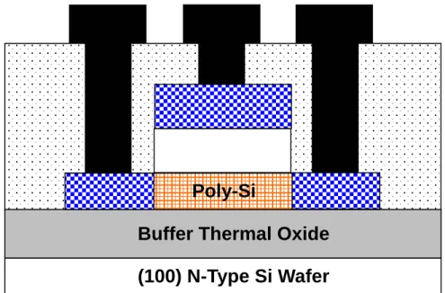
Fig. 3.1 Schematic diagram of the fabrication process for ELA poly-Si TFTs with CF4
plasma treatment. (a) Depositing amorphous silicon and ELA processing. (b) Defining active region and CF4 plasma treatment. (c) S/D implantation and
dopand activation by ELA. (d) Depositing passivation oxide, opening contact holes, depositing metal, and patterning metal.
Fig. 3.2 SIMS profiles of the control and the CF4 plasma-treated ELA poly-Si films.
Fig. 3.3 ESCA profiles of the control and the CF4 plasma-treated ELA poly-Si films.
Fig. 3.4 FTIR spectra of the conventional and the CF4 plasma-treated ELA poly-Si
films.
Fig. 3.5 Transfer characteristics and field-effect mobility versus gate voltage for the control and the CF4 plasma-treated ELA poly-Si TFTs.
Fig. 3.6 Output characteristics of the control and the CF4 plasma treated ELA poly-Si
TFTs.
Fig. 3.7 ln[ID/(VGS-VFB)] versus 1/(VGS-VFB)2 curves at VDS = 0.1V and high VGS for
control and fluorinated ELA poly-Si TFTs.
Fig. 3.8 Density of states (DOS) in the energy band gap of the control and the CF4
plasma-treated ELA poly-Si TFTs.
Fig. 3.9 Cumulative distributions of (a) the time-zero-dielectric-breakdown (TZDB) characteristics (b) leakage current of the gate dielectrics with and without CF4 plasma treatment.
Fig. 3.10 Two accelerating electrical stress tests. (a) hot-carrier stress (HCS), (b) self-heating stress (SHS).
Fig. 3.11 Variations in (a) the On-current and (b) the field-effect mobility as a function of stress time under hot-carrier stress for the control and CF4 plasma-treated
ELA poly-Si TFTs.
Fig. 3.12 Variations in (a) the On-current and (b) the field-effect mobility as a function of stress time under self-heating stress for the control and CF4
plasma-treated ELA poly-Si TFTs.
Chapter 4
with a FSG buffer layer.
Fig. 4.2 SIMS profiles of the as-deposited FSG samples.
Fig. 4.3 Transfer characteristics of the conventional and the proposed poly-Si TFTs with different FSG layers.
Fig. 4.4 SIMS profiles of the conventional and the proposed poly-Si TFTs with different FSG layers.
Fig. 4.5 Trap state density extraction of the conventional and proposed poly-Si TFTs with different FSG layers.
Fig. 4.6 Distribution of (a) filed-effect mobility and (b) leakage current of the poly-Si TFTs on different buffer layers. The vertical bars indicate the minimum and maximum values of the device characteristics and the squares are the average values.
Fig. 4.7 (a) On-current, (b) threshold voltage and (c) field-effect mobility degradation as a function of stress time under hot-carrier stress.
Chapter 5
Fig. 5.1 (a) Schematic diagram of cross-sectional view of poly-Si TFT used in this study. (b) Transfer curves of poly-Si TFT before electrical stress.
Fig. 5.2 Stress gate voltage dependence of Ion degradation of poly-Si TFTs.
Fig. 5.3 Potential barrier for carrier transport raised by filled negative trap states (or charges) in poly-Si channel near drain.
Fig. 5.4 Schematic diagram of traps in drain depletion region and corresponding energy band diagram of Off-stated poly-Si TFT.
Fig. 5.5 Stress gate voltage dependence of Ioff degradation of poly-Si TFTs.
Fig. 5.6 Comparison of electric fields in gate oxide and poly-Si near drain before and after creation of positive oxide charges.
Fig. 5.7 Schematic diagram of our experimental process. The variations in Ion and Ioff
were measured and compared before and after stress under various drain voltages.
Fig. 5.8 Off-current differences vs. drain voltage under various stress conditions, where ∆Ioff = Ioff,stress – Ioff,0.
Fig. 5.9 On-current variations as a function of drain voltage under three stress conditions.
Fig. 5.10 Schematic diagram of effective potential barrier created by trap states near drain under different drain voltages.
Fig. 5.11 Comparison of effective potential barriers created by (a) fixed negative charges and (b) acceptor-like trap states.
Fig. 5.12 Variations of Ion vs. drain voltage for various gate voltages under three stress
conditions (a) VG,stress= 0 V, (b) VG,stress= 10 V and (c) VG,stress= 20 V with
VD,stress = 20 V.
Fig. 5.13 Schematic diagram of device cross-sectional view under three types of stress conditions. Different amounts and spatial distributions of charges trapped in the gate oxide and trap states created in the poly-Si channel lead to different behaviors of the device degradation.
Chapter 6
Fig. 6.1 Equipment setup of scanning capacitance microscopy.
Fig. 6.2 Schematic diagram of SCM scanning on a thin oxide film to detect the defect regions.
Fig. 6.3 (a) Schematic structure of the MOS capacitor fabricated in this study (b) C-V measurements followed by the OBD achieved by the semiconductor parameter analyzer (c) Removal of the poly-Si gate (d) SCM measurements.
Fig. 6.4 (a) High frequency (1MHz) capacitance versus gate voltage (C-V) characteristic swept from inversion to accumulation. (b) J-E characteristics of the thin oxide under –Vg injection.
Fig. 6.5 (a) SCM image and (b) the corresponding AFM image of the fresh oxide film. Fig. 6.6 (a) SCM image and (b) the corresponding AFM image of the oxide film after
OBD.
Fig. 6.7 Enlargement of SCM images for (a) fresh oxide film and (b) oxide film with a single OBD spot.
Fig. 6.8 Enlargement of SCM image for an oxide sample with three OBD spots Fig. 6.9 Corresponding roughness (RMS) distributions of the oxide layer with OBD. Fig. 6.10 Enlarged SCM image of one OBD spot and a cross-sectional view of the low
Table Lists
Chapter 2
Table 2.1 Comparison of device characteristics of the control and fluorinated SPC poly-Si TFTs.
Chapter 3
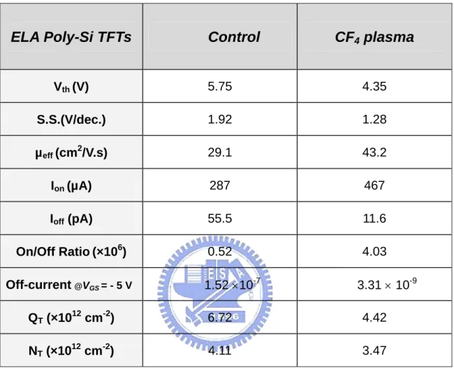
Table 3.1 Comparison of the extracted device parameters for the control and the CF4
plasma-treated ELA poly-Si TFTs.
Chapter 4
Table 4.1 Conditions of gas flow rates to deposit FSG buffer layers.
Table 4.2 Comparison of device characteristics of the conventional and the proposed ELA poly-Si TFTs (W/L = 40μm/10μm).
Chapter 1
Introduction
1.1
Overview of Poly-Si Thin-Film Transistors
Thin-film transistors (TFTs) have been widely used in static random access memories (SRAMs) [1], electrical erasable programming read only memories (EEPROMs) [2], linear image sensors [3], thermal printer heads [4], photodetector amplifier [5], scanner [6], and active matrix liquid crystal displays (AMLCDs) [7]-[9]. Over the past decade, the thriving growth of the flat-penal-displays (FPDs) industry has become the main driving force in the development of the TFTs technology. Currently, AMLCD is believed to be the most promising candidate to realize large-area FPDs with high resolution. Conventionally, amorphous silicon (a-Si) TFTs are used for the pixel switching elements. However, due to their low electron mobility ( ≤1 cm2/Vs), it is hard to realize the integration of the switching pixels with the peripheral driver circuits in one signal substrate to further reduce the production cost of AMLCDs. In 1966, the first polycrystalline silicon thin film transistors (Poly-Si TFTs) were fabricated by C. H. Fa et al. [10]. In comparison with a-Si TFTs, poly-Si TFTs have a superior carrier mobility, higher CMOS capability, and better reliability [11]-[27].
The high driving current of poly-Si TFTs makes the integration of switching pixels and driver circuits possible [11]. Moreover, the aperture ratio and the panel brightness can be also greatly promoted due to small device size needed using poly-Si TFTs [12]. Therefore, the performance of display can be significantly improved. As a
result, poly-Si TFTs have a great potential to realize high-performance large-area AMLCDs applications, and further to accomplish System-on-Panel (SOP).
Process temperature is one of the most important concerns to fabricate poly-Si TFTs on inexpensive, low-melting point and large-area glass substrates. Many crystallization techniques have been proposed to achieve low temperature polycrystalline silicon (LTPS) TFTs (≤ 620℃), such as solid phase crystallization (SPC) [13]-[16], laser annealing crystallization [17]-[21], metal induced crystallization (MIC) [22]-[24], and metal-induced lateral crystallization (MILC)[25]-[27]. In such low temperatures, the quality of poly-Si films plays a critical role in the device performance and reliability. Among these techniques, excimer laser annealing (ELA) is believed to become the mainstream technology for mass production because high-quality poly-Si films can be obtained.
Compared to single crystal silicon, poly-Si is rich in grain boundary defects and intra-grain defects, resulting in numerous trap states. Trap states in the TFT’s channel can trap carriers to generate barriers for carrier transport when TFT is turned on, lowering the device’s diving current [28]. As the device is off, large trap states enhance the traps-assisted tunneling near the drain, causing a large leakage-current [29]. That is to say, the electrical properties of poly-Si TFT’s is strongly related to the amount of defects. Two methods have been developed to reduce the defect density. One is enlarging the poly-Si grain size [30], [31]. This can reduce the number of grain boundaries within the channel and therefore improve the device performance. The other is plasma treatments. Radicals existed in plasmas can terminate defects in the poly-Si, and thus reduce the trap state density. Recently, various plasmas such as H2
[32], NH3 [33], N2O [34] and O2 plasmas [35] have been intensely investigated to
accomplish this goal.
high-performance poly-Si TFTs. This technique focuses on the reduction of the electric field near the drain junction, and thus suppresses the device’s Off-state leakage current. Many structures including multiple channel structures [36], offset drain/source [37], [38], lightly doped drain (LDD) [39], gate-overlapped LDD [40]-[42], field induced drain [43] and vertical channel [44] have been proposed and investigated intensively.
1.2
Motivation
In the poly-Si TFT’s channel, trap states, resulted from grain boundary and intra-grain defects, can trap carriers to form potential barriers, and thus affect the current transport [28]. Moreover, the Off-current in poly-Si TFTs is associated with the amount of trap states in the drain depletion region. The generation of it can be attributed to thermionic emission at a low electric field and the field-enhanced emission (i.e. F-P emission or trap-assisted band-to-band tunneling) at a high electric filed [29]. Hence, trap states can lead to a poor device performance, such as low field-effect mobility, large leakage current, bad subthreshold slope and high threshold voltage.
Plasma treatments are believed to be the most effective methods to reduce trap states in the poly-Si. Many kinds of plasma such as H2/N2 mixture plasma [45],
nitrogen implantation with H2 plasma [33], pre-oxidation NH3 annealing with H2
plasma [33], NH3 plasma [46] and H2/O2 plasma [47] have been proposed. Generally,
hydrogen-based plasmas are mostly adopted, because the hydrogen atoms can easily restore the trap states at the poly-Si/SiO2 interface and in the grain boundaries.
However, it is known that hydrogenated poly-Si TFTs have a troublesome issue in the device reliability [48], [49]. The device performance degrades seriously under a
long-term electrical stress. It is known that the poor device reliability of the hydrogenated TFTs is due to the weak Si-H bonds, which might be broken easily during the electrical stress and thus cause the creation of trap states in the poly-Si channel [50]. Recently, fluorination technique has been proposed. It can improve both the device performance and also reliability, because the Si-F bonds are rather strong than Si-H bonds [51]-[56]. In conventional, fluorine ion implantation (FII) technique is mostly adopted to introduce fluorine atoms into the poly-Si. However, this method may be not suitable for large-area electronics. Moreover, a subsequent high temperature process, required to activate implanted fluorine atoms and recover the damage created by implantation, is also not compatible with the current AMLCD fabrication processes. Therefore, effective and process-compatible techniques to introduce fluorine atoms into the poly-Si channel are needed to be developed. In Chapters 2, 3 and 4, new process-compatible fluorination techniques are demonstrated and investigated.
Moreover, it is known that studying the instabilities of the device characteristics in poly-Si TFTs is more complicated than doing so in the case of single-crystal MOSFETs, which is due to the random distribution of grain boundaries and the poor quality of the gate oxide. From the previous reports in studying single-crystal MOSFETs, we believe that the amounts and the spatial distributions of the trap states (or charges) in the gate oxide and in the poly-Si play important roles in the instabilities of poly-Si TFTs. On-current (Ion) and Off-current (Ioff) are two of the most
important parameters in designing poly-Si TFT circuits, related to the driving capacity and the charge storage, which are very sensitive to the oxide trap charges and trap states in the poly-Si. Their instabilities, particularly with regard to the electrical stress, have constrained poly-Si TFTs applications. Although several groups have studied the variations in the device characteristics of poly-Si TFTs at the On-state or Off-state
after the electrical stress separately [49], [57], [58], a comprehensive mechanism for the degradation of both Ion and Ioff under various stress conditions is not yet well
known. In Chapter 5, a new strategy for studying the mechanism of the Ion and Ioff
instabilities in poly-Si is adopted.
In addition, due to the continuous scaling down of metal-oxide-semiconductor field-effect transistors (MOSFETs), the quality of the thin gate oxide has become more and more important. Oxide breakdown (OBD) is one of the most critical concerns for integrated circuit device reliability [59], [60]. The OBD process is thought to be a local phenomenon within the nano-scale region, not occurring throughout the total oxide area [61], [62]. However, conventional electrical measurements, made through MOS capacitors, only detect general information about the whole oxide area under the electrode, and the localized OBD behavior is missed. To characterize the localized OBD evens in detail, highly sensitive measurement tools with a good spatial resolution are necessary. Scanning capacitance microscopy (SCM), combined with atomic force microscopy (AFM), has been used to study local charge trapping in gate oxides and dynamic device operation images [63], [64], which is a powerful technique to synchronously measure the differential capacitance (dC/dV) images and the corresponding topographic images of thin films. Thus, in Chapter 6, we demonstrate a new technique for mapping oxide breakdown spots by adopting SCM with corresponding AFM images.
1.3
Thesis Organization
This thesis is organized as follow:
In Chapter 1, the overview of poly-Si TFTs and motivations of this thesis are described.
In Chapter 2, a novel fluorine-based plasma treatment, CF4 plasma treatment, is
employed to treat the solid-phase-crystallized (SPC) poly-Si TFT. The electrical characteristics and reliability of the CF4 plasma-treated poly-Si TFTs are explored.
The fluorine passivation effect on SPC ploy-Si TFTs using CF4 plasma is investigated.
In Chapter 3, CF4 plasma treatment, combined with excimer laser annealing
(ELA), is proposed to fabricate CF4 plasma-treated ELA poly-Si TFTs. The electrical
characteristics as well as the device reliability of the ELA poly-Si TFTs are greatly improved. The mechanisms responsible to the device improvements are comprehensively discussed.
In Chapter 4, fabricating poly-Si TFTs on an FSG buffer layer is proposed and demonstrated. Experimental results reveal that remarkably improved device performance and uniformity can be achieved with appropriate fluorine incorporation in the poly-Si. Furthermore, the fluorine also increases the poly-Si TFTs reliability against hot carrier stressing, which is attributed to the formation of Si-F bonds. However, too much fluorine incorporation causes an unwanted degradation phenomenon. The relation between the device characteristics and the amount of fluorine incorporated is analyzed.
In Chapter 5, the Ion and Ioff instabilities of poly-Si TFTs are investigated under
various electrical stress conditions. The stress-induced device degradation is studied by measuring the dependences of Ion and Ioff on the drain/gate voltages. From the
experimental results, dissimilar variations in Ion and Ioff are observed, which can be
attributed to the variances in the amount of trap charges in the gate oxide and the spatial distributions of the trap states generated in the poly-Si channel. A comprehensive model for the degradation of Ion and Ioff in poly-Si TFTs under various
stress conditions is presented.
force microscopy (AFM), is employed to investigate the dielectric breakdown phenomena in thin SiO2 films. The localized breakdown spots can be clearly imaged
by SCM. Moreover, these breakdown spots are carefully analyzed, which exhibit signals with low differential capacitance (dC/dV) signals.
In Chapter 7, conclusions of this thesis and recommendations for further research are given.
References:
[1] T. Yamanaka, T. Hashimoto, N. Hasegawa, T. Tanaka, N. Hashimoto, A. Shimizu, N. Ohki, K. Ishibashi, K. Sasaki, T. Nishida, T. Mine, E. Takeda and T. Nagano, “ Advanced TFT SRAM cell technology using a phase-shift lithography,” IEEE
Trans. Electron Devices, vol. 42, no. 7, pp. 1305-1313, 1995.
[2] N. D. Young, G. Harkin, R. M. Bunn, D. J. McCulloch and I. D. French, “The fabrication and characterization of EEPROM arrays on glass using a low temperature poly-Si TFT process,” IEEE Trans. Electron Devices, vol. 43, no. 11 pp. 1930-1936, 1996.
[3] T. Kaneko, Y. Hosokawa, M. Tadauchi, Y. Kita and H. Andoh, “400 dpi integrated contact type linear image sensors with poly-Si TFT’s analog readout circuits and dynamic shift registers,” IEEE Trans. Electron Devices, vol. 38, no. 5 pp. 1086-1096, 1991.
[4] Y. Hayashi, H. Hayashi, M. Negishi and T. Matsushita, “A thermal printer head with CMOS thin-film transistors and heating elements integrated on a chop,”
IEEE Solid-State Circuits Conference (ISSCC), pp. 266, 1988.
[5] N. Yamauchi, Y. Inada and M. Okamura, “An intergated photodetector-amplifier using a-Si p-i-n photodiodes and poly-Si thin-film transistors,” IEEE Photonic
Tech. Lett., vol. 5, pp. 319, 1993.
[6] M. G. Clark, “Current status and future prospects of poly-Si,” IEE Proc. Circuits
Devices Syst., vol. 141, no. 1, pp. 3, 1994.
[7] Y. Oana, “Current and future technology of low-temperature poly-Si TFT-LCDs,”
Journal of the SID, vol. 9, pp. 169-172, 2001.
[8] S. Morozumi, K. Oguchi, S. Yazawa, Y. Kodaira, H. Ohshima, and T. Mano, “B/W and color LC video display addressed by poly-Si TFTs,” in SID Tech. Dig.,
pp.156, 1983.
[9] R. E. Proano, R. S. Misage, D. Jones, and D. G. Ast, “Guest-host active matrix liquid-crystal display using high-voltage polysilicon thin film transistors,” IEEE
Trans. Electron Devices, vol. 38, pp. 1781, 1991.
[10] C. H. Fa, and T. T. Jew, “The polysilicon insulated-gate field-effect transistor,”
IEEE Trans. Electron Devices, vol. 13, no. 2, pp. 290, 1966.
[11] W. G. Hawkins, “Polycrystalline-silicon device technology for large-area electronics,” IEEE Trans. Electron Devices, vol. 33, pp. 477-481, 1986.
[12] I. -W. Wu, “Cell design considerations for high-aperture-ratio direct-view and projection polysilicon TFT-LCDs,” in SID Tech. Dig., pp. 19, 1995.
[13] A. Nakamura, F. Emoto, E. Fujii and A. Tamamoto, “A high-reliability, low-operation-voltage monolithic active-matrix LCD by using advanced solid-phase growth technique,” in IEDM Tech. Dig., pp.847, 1990.
[14] R. B. Iverson and R. Reif, “Recrystallization of amorphized polycrystalline silicon films on SiO2: temperature dependence of the crystallization parameters,” J. Appl. Phys., vol. 62, no. 5, pp. 1675-1681, 1987.
[15] F. Emoto, K. Senda, E. Fujii, A. Nakamura, A. Yamamoto, Y. Yamamoto, Y. Uemoto, and Gota Kano, “ Solid phase growth technique for hogh cut-off frequency polysilicon TFT integrated circuits on a quartz substrate,” IEEE Trans.
Electron Devices, vol. 37, pp. 1462, 1990.
[16] M. K. Hatalis and D. W. Greve, “Large grain polycrystalline silicon by low-temperature annealing of low-pressure chemical vapor deposited amorphous silicon films,” J. Appl. Phys., vol. 63, no. 7, pp. 2260-2266, 1988.
[17] G. K. Guist, and T. W. Sigmon, “High-performance laser-processed polysilicon thin-film transistors,” IEEE Electron Device Lett., vol. 20, no. 2, pp. 77-79, 1999. [18] N. Kudo, N. Kusumoto, T. Inushima, and S. Yamazaki, “Characterization of
polycrystalline-Si thin-film transistors fabricated by excimer laser annealing method,” IEEE Trans. Electron Devices, vol. 41, no. 10, pp. 1876-1879, 1994. [19] T. Sameshima, S. Usui and M. Sekiya, “XeCl excimer laser annealing used in the
fabrication of poly-Si TFT’s,” IEEE Electron Device Lett., vol. 7, no. 5, pp. 276-278, 1986.
[20] D. H. Choi, E. Sadauyki, O. Sugiura and M. Matsumra, “Excimer-laser crystallized poly-Si TFT’s with mobility more than 600 cm2/V.s,” IEEE Trans.
Electron Devices, vol. 40, no. 11, pp. 2129, 1993.
[21] K. Shimizu, O. Sugiura and M. Matsumra, “High-mobility poly-Si thin-film transistors fabricated by a novel excimer laser crystallization method,” IEEE
Trans. Electron Devices, vol. 40, no. 1, pp. 112-117, 1993.
[22] S. Y. Yoon, K. Hyung, C. O. Kim, J. Y. Oh and J. Jang, “Low temperature metal induce crystallization of amorphous silicon using a Ni solution,” J. Appl. Phys., vol. 82, pp. 5865-5867, 1997.
[23] G. Radnoczi, A. Robertsson, H. T. G.. Hentzell, S. F. Gong and M. A. Hasan, “Al induced crystallization of a-Si,” J. Appl. Phys., vol. 69, pp. 6394-6399, 1991. [24] Z. Jin, G. A. Bhat, M. Yeung, H. S. Kwok and M. Wong, “Nickel induced
crystallization of amorphous silicon thin films,” J. Appl. Phys., vol. 84, pp.194-200, 1998.
[25] S. W. Lee and S. K. Joo, “Low temperature poly-Si thin-film transistor fabrication by metal-induced lateral crystallization,” IEEE Electron Device Lett., vol. 17, pp. 160-162, 1996.
[26] H. Kim, J. G. Couillard and D. G. Ast, “Kinetic of silicide-induced crystallization of polycrystalline thin-film transistors fabricated from amorphous chemical-vapor deposition silicon,” Appl. Phys. Lett., vol. 72, pp. 803-805, 1998. [27] Z. Jin, H. S. Kwok and M. Wong, “Performance of thin-film transistors with
ultrathin Ni-NILC polycrystalline silicon channel layers,” IEEE Electron Device
Lett., vol. 20, pp. 167-169, 1999.
[28] G. Y. Yang, S. H. Hur and C. H. Han, “A physical-based analytical turn-on model of polysilicon thin-film transistors for circuit simulation,” IEEE Trans. Electron
Devices, vol. 46, pp. 165-172, 1999.
[29] K. R. Olasupo and M. K, Hatalis, “Leakage current mechanism in sub-micron polysilicon thin-film transistors,” IEEE Trans. Electron Devices, vol. 43, pp. 1218-1223, 1996.
[30] C. H. Hong, C. Y. Park and H. J. Kim, “Structure and crystallization of low-pressure chemical vapor deposited silicon films using Si2H2 gas,” J. Appl. Phys., vol. 71, pp.5427-5432, 1992.
[31] J. H. Jeon, M. C. Lee, K. C. Park, M. K. Han, “A new polycrystalline silicon TFT with a single grain boundary in the channel,” IEEE Electron Device Lett., vol. 22, no. 9, pp. 429-431, 2001.
[32] A. Yin, and S. J. Fonash, “High-performance p-channel poly-Si TFT’s using electron cyclotron resonance hydrogen plasma passivation,” IEEE Electron
Device lett., vol. 15, no. 12, pp. 502-503, 1994.
[33] C. K. Yang, T. F. Lei, C. L. Lee, “The combined effects of low pressure NH3
annealing and H2 plasma hydrogenation on polysilicon thin-film-transistors,” IEEE Electron Device lett., vol. 15, pp. 389-390, 1994.
[34] J. W. Lee, N. I. Lee, J. I. Kan, C. H. Han, “Characteristics of polysilicon thin-film transistor with thin-gate dielectric grown by electron cyclotron resonance nitrous oxide plasma,” IEEE Electron Device lett., vol. 18, pp. 172-174, 1997.
[35] K. C. Moon, J. H. Lee, M. K. Han, “Improvement of polycrystalline silicon thin film transistor using oxygen plasma pretreatment before laser crystallization,”
IEEE Trans. Electron Devices, vol. 49, pp. 1319-1322, 2002.
[36] T. Unagami and O. Kogure, “Large on/off current ratio and low leakage current poly-Si TFTs with multichannel structure,” IEEE Trans. Electron Devices, vol. 35, no. 11, pp. 1986-1989, 1988.
[37] B. H. Min, C. M. Park and M. K. Han, “A novel offset gated polysilicon thin film transistor without an additional offset mask,” IEEE Electron Device lett., vol. 16, no. 5, pp. 161-163, 1995.
[38] Z. Xiong, H. Liu, C. Zhu and Sin, J.K.O., “Characteristics of high-K spacer offset-gated polysilicon TFTs,” IEEE Trans. Electron Devices, vol. 51, no. 8, pp. 1304-1308, 2004.
[39] P. S. Shih, C. Y. Chang, T. C. Chang, T. Y. Huang, D. Z. Peng and C. F. Yeh, “A novel lightly doped drain polysilicon thin-film transistor with oxide sidewall spacer formed by one-step selective liquid phase deposition,” IEEE Electron
Device lett., vol. 20, no. 8, pp. 421-423, 1999.
[40] K. Y. Choi and M. K. Han, “A novel gate-overlapped LDD poly-Si thin-film transistor,” IEEE Electron Device lett., vol. 17, no. 12, pp. 566-568, 1996.
[41] A.Bonfiglietti, M. Cuscuna, A.Valletta, L. Mariucci, A. Pecora, G. Fortunato, S. D. Brotherton and J. R. Ayres, “Analysis of electrical characteristics of gate overlapped lightly doped drain (GOLDD) polysilicon thin-film transistors with different LDD doping concentration,” IEEE Trans. Electron Devices, vol. 50, no. 12, pp. 2425-2433, 2003.
[42] Y. Mishima and Y. Ebiko, “Improved lifetime of poly-Si TFTs with a self-aligned gate-overlapped LDD structure,” IEEE Trans. Electron Devices, vol. 49, no. 6, pp. 981-985, 2002.
[43] H. C. Lin, C.-M Yu, C.-Y. Lin, K.-L.Yeh, T. Y. Huang and T. F. Lei, “A novel thin-film transistor with self-aligned field induced drain,” IEEE Electron Device
lett., vol. 22, no. 1, pp. 26-28, 2001.
[44] C. S. Lai, C. L. Lee, T. F. Lei and H. N. Chern, “A novel vertical bottom-gate polysilicon thin film transistor with self-aligned offset,” IEEE Electron Device
lett., vol. 17, no. 5, pp. 199-201, 1996.
[45] M. J. Tasi, F. S. Wang, K. L. Cheng, S. Y. Wang, M. S. Feng, and H. C. Chen, “Characterization of H2/N2 plasma passivation process for poly-Si thin-film
transistors (TFTs),” Solid State Electronics, vol. 38, no. 5, pp.1233-1238, 1995 [46] H. C. Cheng, F. S. Wang, and C. Y. Huang, “Effects of NH3 plasma passivation
on n-channel Polycrystalline silicon thin-film-transistors,” IEEE Trans. Electron
Devices, vol. 44, no. 1, pp. 64-68, 1997.
[47] H. N. Chern, C. L. Lee, and T. F. Lei, “H2/O2 plasma on polysilicon thin film transistor,” IEEE Electron Device Lett., vol. 14, pp.115-117, 1993.
[48] C. W. Lin, M. Z. Yang, C. C. Yeh, L. J. Cheng, T. Y. Huang, H. C. Cheng, H. C. Lin, T. S. Chao and C. Y. Chang, “Effects of plasma treatments, substrates type, and crystallization methods on performance and reliability of low temperature polysilicon TFTs” in IEDM Tech. Dig., pp.305, 1999.
[49] I.-W. Wu, W. B. Jackson, T.-Y. Huang, A. G. Lewis and A. Chiang, “Mechanism of device degradation in n- and p-channel polysilicon TFT’s by electrical stressing,” IEEE Electron Device Lett., vol. 11, no. 4, pp. 167-170, 1990.
[50] M. Hack, A. G. Lewis, and I.-W. Wu, “Physical models for degradation effects in polysilicon thin-film transistors,” IEEE Trans. Electron Devices, vol. 40, pp. 890-897, 1993.
[51] H. N. Chern, C. L. Lee, and T. F. Lei, “The effects of fluorine passivation on polysilicon thin film transistors,” IEEE Trans. Electron Devices, vol. 41, pp.
698-702, May 1994.
[52] S. Maegawa, T. Ipposhi, S. Maeda, H. Nishimura, T. Ichiki, M. Ashida, O. Tanina, Y. Inoue, T. Nishimura and N. Tsubouchi, “Performanc and reliability improvements in poly-Si TFT’s by fluorine implantation into gate poly-Si,”
IEEE Trans. Electron Devices, vol. 42, pp. 1106-1111, June 1995.
[53] J. W. Park, B. T. Ahn, and K. Lee, “Effects of F+ implantation on the characteristics of poly-Si films and low-temperature n-ch poly-Si thin-film transistors,” Jpn. J. Appl. Phys., vol. 34, pp. 1436-1441, Mar. 1995.
[54] C. H. Fan and M. C. Chen, “Performance improvement of excimer laser annealed Poly-Si TFTs using fluorine ion implantation” Electrochemical and Solid State
Lett., vol. 5, pp. G75-G77, 2002.
[55] C. H. Kim, S. H. Jung, J. S. Yoo, and M. K. Han, “Poly-Si TFT fabricated by laser-induced in-situ fluorine passivation and laser doping,” IEEE Electron
Device lett., vol. 22, pp. 396-398, Aug. 2001.
[56] C. A. Dimitriadis, P. A. Coxon, L. Dozsa, L. Papadimitriou, and N. Economou, “Performance of thin-film transistors on polysilicon films grown by low-pressure chemical vapor deposition at various pressures,” IEEE Trans. Electron Devices, vol. 39, pp. 598-606, Mar. 1992.
[57] F. V. Farmakis, J. Brini, G. Kamarinos and C. A. Dimitriadis, “Anomalous turn-on voltage degradation during hot-carrier stress in polycrystalline silicon thin-film transistors,” IEEE Electron Device Lett., vol. 22, no. 2, pp. 74-76, 2001. [58] G. Fortunato, A. Pecora, G. Tallarida, L. Mariucci, C. Reita and P. Migliorato, “Hot carrier effects in n-channel polycrystalline silicon thin-film transisitors: A correlation between off-current and transconductance variations,” IEEE Trans.
[59] B. Kaczer, R. Degraeve, M. Rasras, K. Van de Mieroop, P. J. Roussel, G.. Groeseneken, “Impact of MOSFET gate oxide breakdown on digital circuit operation and reliability,” IEEE Trans. Electron Devices, vol. 49, no.3, pp. 500-506, 2002.
[60] J. S. Suehle, “Ultrathin gate oxide reliability: physical models, statistics, and characterization,” IEEE Trans. Electron Devices, vol. 49, no.6, pp. 958-971, 2002.
[61] M. Nafria, J. Sune, and X. Aymerich, “Exploratory observations of post-breakdown conduction in polycrystalline-silicon and metal-gated thin-oxide metal-oxide-semiconductor capacitors,” J. Appl. Phys., vol. 73, pp. 205-215, 1993.
[62] S. Lombardo, A. La Magna, C. F. Spinella, C. Gerardi, and F. Crupi, “Degradation and hard breakdown transient of thin gate oxides in metal–SiO2–Si
capacitors: Dependence on oxide thickness,” J. Appl. Phys., vol. 86, pp. 6382-6391, 1999.
[63] J. W. Hong, S. M. Shin, C. J. Kang, Y. Kuk, Z. G. Khim, and S. Park, “Local charge trapping and detection of trapped charge by scanning capacitance microscope in the SiO2/Si system,” Appl. Phys. Lett., vol. 75, pp. 1760-1762,
1999.
[64] C. Y. Nakakura, D. L. Hetherington, M. R. Shaneyfelt, P. J. Shea and A. N. Erikson, “Observation of metal–oxide–semiconductor transistor operation using scanning capacitance microscopy,” Appl. Phys. Lett., vol. 75, pp. 2319-2321, 1999.
Chapter 2
CF
4Plasma Treatment on
Solid-Phase-Crystallized (SPC) Poly-Si TFTs
2.1 Introduction
In comparison with conventional a-Si TFTs, poly-Si TFTs have many advantages including high driving current, superior carrier mobility and great CMOS capability, which make the integration of switching-pixels and their peripheral driver circuits on a single glass substrate possible. It is known that trap states in the poly-Si can degrade the carrier transport and also increase the device leakage current [1], [2]. To eliminate these trap states has become the main topic for the current and future production of high performance poly-Si TFTs. Conventionally, hydrogen-based plasma treatment is the most popular method to passivate trap states in the current production [3], [4]. Although hydrogenation can eliminate the intra-grain and grain boundary trap states in the poly-Si film, the hydrogenated poly-Si TFTs suffer from a serious reliability issue, which can be attributed to the weak Si-H bonds.
Recently, several studies have demonstrated the use of fluorine (F) atoms to passivate the poly-Si films, which can improve both the performance and reliability of poly-Si TFTs, particularly when devices are under long-term electrical stress tests [5]-[9]. It is known that fluorine atoms can terminate dangling bonds and replace weak bonds in the grain boundaries and SiO2/poly-Si interface and thus reduce the
trap states in the poly-Si channel. In addition, the strong Si-F bonds, more stable than Si-H bonds, can greatly improve the device reliability under an electrical stress.
Fluorine ion implantation (FII), the most adoptive fluorinating technique, has been widely investigated [5]-[8]. It is worth noting that ion implantation technique is not suitable for large-sized glass substrate. Moreover, a subsequent high temperature annealing to recover the defects created by FII is required in this method, which is not compatible with current production. Therefore, C. H. Kim et al. demonstrated the use of fluorinated oxide (SiOxFy) to replace FII, which can be served as a diffusion source
[9]. However, this technique increases manufacturing processes since extra film deposition and etching are required.
To date, although the effects of fluorination have been clarified, there is still a lack of a process-compatible technique to effectively introduce fluorine atoms into poly-Si films. In this chapter, we proposed a new fluorine passivation technique by employing CF4 plasma treatment, which is a simply and efficient process. To avoid an
unwanted etching effect, we controlled the RF to apply a very low power (5 Watts) to dissociate fluorine atoms, which were used to fluorinate the poly-Si film. Using this technique, the fluorinated poly-Si TFTs have been fabricated and the device characteristics and reliability were investigated.
2.2 Experimental
The schematic diagram of the fabrication process is illustrated in Fig. 2.1. First, a 100-nm-thick amorphous-silicon layer was deposited on thermally oxidized Si wafer by dissociation of SiH4 gas in a low-pressure chemical vapor deposition (LPCVD) at
550°C. Subsequently, solid phase crystallization (SPC) was performed at 600°C for 24 hours in N2 ambient for the phase transformation. Individual active regions were
then patterned and defined. After a standard RCA cleaning, samples were subjected to the CF4 plasma treatment, conducted in a plasma-enhanced chemical vapor deposition
(PECVD) system at 350°C for 15 seconds, with a pressure of 200 mTorr and a power of 5 Watts. Then, a 50-nm-thick tetraethyl orthosilicate (TEOS) oxide was deposited to serve as the gate insulator and a 200-nm-thick poly-Si film was deposited and patterned for the gate electrode. A self-aligned phosphorous ion implantation was preformed with the dosage and energy of 5×1015 cm-2 and 40 KeV, respectively. The dopant activation was performed at 600°C furnace annealing at N2 ambient for 24
hours, followed by a deposition of the passivation layer and a definition of contact holes. Finally, a 500-nm-thick Al electrode was deposited and patterned. The control samples were prepared without the fluorinating process. To concentrate on revealing the fluorine passivation effects of the CF4 plasma treatment, none of additional
hydrogenation process was performed on the control samples. The electrical and reliability characteristics were performed by using HP 4156B.
2.3 Results and Discussion
2.3.1 Comparison of Device Characteristics
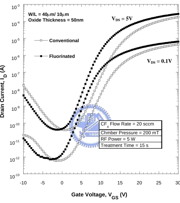
Figure 2.2(a) shows the transfer characteristics (ID-VGS) for the control and
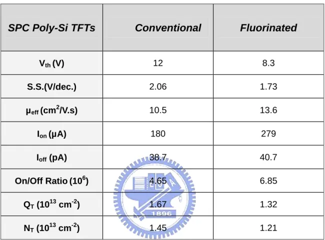
fluorinated poly-Si TFTs. The measurements were performed at two different drain voltages of VDS = 0.1 V and 5 V. The parameters of the devices, including the
threshold voltage (Vth) and subthreshold swing (S.S.), maximum On-current (Ion) and
the minimum Off-current (Ioff) were measured at VDS = 5 V. The threshold voltage is
defined as the gate voltage required to achieve a normalized drain current of ID =
(W/L) ×100 nA. Accordingly, the performance of the fluorinated poly-Si TFT is significantly improved. The Vth and S.S. of the fluorinated poly-Si TFT were found to
be 8.3 V and 1.73 V/dec., which are superior to those of the control one (12 V and 2.06 V/dec., respectively). It’s known that the Vth and S.S. are strongly influenced by
the deep trap states, associated with dangling bonds in the channel, which have energy states near the middle of the silicon band gap. Therefore, one can infer that CF4
plasma treatment can terminate the dangling bonds in the poly-Si and SiO2/poly-Si
interface. Additionally, the Ion and On/Off current ratio of the fluorinated TFT are also
better than those of the control TFT.
The minimum Off-current of the fluorinated device is nearly unsuppressed, which is consistent with the previous reports by Chern et al. [6] and Kim et al. [9] However, while the applied gate voltage was toward more negative (VGS < -2 V ), the
fluorinated poly-Si TFT shows smaller leakage current compared with that of the control TFT. It is known that under a high electric field leakage current of the poly-Si TFT mainly comes from the trap-assisted band to band tunneling near the drain edge [10]. This observation suggests that there must be fewer trap states existed in the fluorinated poly-Si TFT, and thus the leakage current under a high electric field is reduced.
Figure 2.2(b) shows field-effect mobility versus the gate voltage of control and fluorinated poly-Si TFTs. The field-effect mobility was calculated from the value of transconductance at VDS = 0.1V. The fluorinated poly-Si TFT shows approximately
22.8 % enhancement in the maximum field-effect mobility. Note that the field-effect mobility is significantly affected by the tail states near the band edge, which is resulted from the strain bonds in poly-Si and SiO2/poly-Si interface [1]. These results
imply that the CF4 plasma treatment may not only terminate the dangling bonds, but
also relieve the strain bonds. The extracted device parameters are listed in Table 2.1.
2.3.2 Extraction of Trap State Density
The grain boundary trap state densities (QT) of the conventional and fluorinated
exhibits the plots of the ln[ID/(VGS-VFB)] versus 1/(VGS-VFB)2 curves at low VDS and
high VGS. The QT was extracted from the slopes of these curves. The fluorinated
poly-Si TFT exhibits a QT of 1.32×1013 cm-2, whereas the control TFT has 1.67×10¹³
cm-2. This result implies that the CF4 plasma treatment can terminate the grain
boundary trap states in the poly-Si film. To further study the fluorine passivation effect near the interface, the effective interface trap states densities (NT) near the
SiO2/poly-Si interface were also calculated. From the S.S., by neglecting the depletion
capacitance, the Nt can be expressed as[13]:
NT = [(S.S./ln 10)(q / kT)-1)](Cox/q) (1)
where the Cox is the capacitance of the gate oxide. The NT of the control TFT and
the fluorinated TFT are 1.45 × 10¹³
cm-2 and 1.21 × 1013 cm-2, respectively. The NT
values reflect trap states near the SiO2/poly-Si interface.
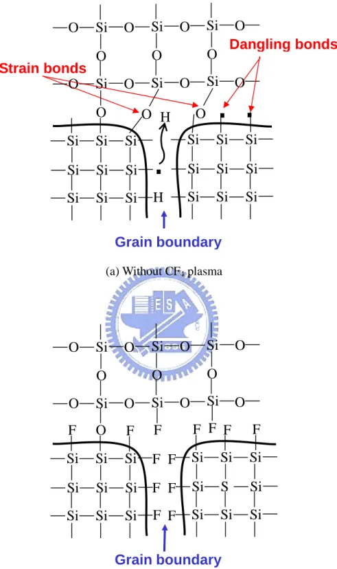
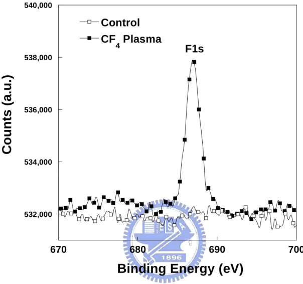
Figure 2.4 shows the SIMS (secondary ion mass spectroscopy) profiles of the control and fluorinated poly-Si films. The SIMS profiles exhibit that substantial amount of fluorine were introduced into the poly-Si layer by CF4 plasma treatment,
not carbon atoms. The SIMS analysis also shows a notably high concentration of fluorine atoms piling up near the SiO2/poly-Si interface, instead of in the deep ploy-Si
layer. These piled-up fluorine atoms is believed that they can provide more effective passivation of trap states, because the quality of SiO2/poly-Si interface are the main
issue for carrier transport.
Therefore, these results figure that trap states in both grain boundaries and the SiO2/poly-Si interface were reduced by using CF4 plasma treatment, which resulting
the great improvement in the device performance. Based on these results, a schematic cross section view of the SiO2/poly-Si interface is illustrated in Fig. 2.5. It is
2.3.3 Output Characteristics and Activation Energy
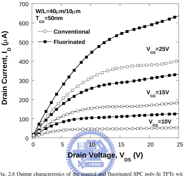
Figure 2.6 shows the output characteristics (ID-VDS) of the fluorinated and
control poly-Si TFTs. As can be seen, the driving current increases significantly for the fluorinated poly-Si TFT compared with that of the control TFT. This is due to the higher mobility and smaller threshold voltage of the fluorinated poly-Si TFT. The driving current increased 130%, 84% and 55% at VDS= 20 V with VGS= 10 V, 15 V
and 25 V, respectively.
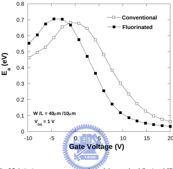
Figure 2.7 exhibits the activation energy (Ea) versus the gate voltage for the
control and fluorinated poly-Si TFTs at VDS = 1 V. In Off-region (low VGS), the value
of Ea reflects the required energy for carriers to leak by means of traps, whereas in
On-region (high VGS), the value of Ea reflects the carrier transport barrier caused by
the trap states within the poly-Si channel [14]. Compared with the control TFT, the extracted Ea of the fluorinated poly-Si TFT decreases in On-region and increases in
Off-region. That is to say, for fluorinated poly-Si TFT, fluorine atoms can passivate the trap states and hence reduce the barrier height for carrier transport when device is turned on. On the other hand, in Off-region fewer trap states after fluorinating process resulting in the increasing of Ea and thus the trap-assisted leakage current is
suppressed. Moreover, in the subthreshold region, a steeper profile can be found for the fluorinated TFT, which proves that the interface quality of the fluorinated TFT is much better than that of the control TFT.
2.3.4 Device Reliability
Additionally, the hot carrier stress was carried out to examine the reliability of the device. The device degradation under hot carrier stress can be attributed to two mechanisms: oxide trap charges and the creation of trap states in the poly-Si. This can be attributed to channel-hot-electron (CHE) and self-heating (SH) phenomenon. For
CHE, electrons were injected and trapped in the gate oxide; then, the carrier flow in the channel is disturbed, therefore reducing the Ion. SH-induced damage is due to the large Joule heat, resulted from a high drain current [15], [16]. Because TFTs are fabricated on a poor thermal-conducting substrate, devices can reach a very high temperature during operation. Such high temperature enhances bonds breaking to generate trap states in the poly-Si, and thus degrade the TFT performance.
Figure 2.8 shows the variation of On-current under a hot carrier stress. The stress condition is performed at VDS=30V and VGS=30V for 4500 s. The variation in Ion is
defined as (Ion,stressed–Ion,initial)/ Ion,initial×100%, where the Ion,initial and Ion,stressed are the
measured Ion prior to and after the electrical stress. As can be seen, the fluorination
process can greatly alleviate the On-current degradation under a hot carrier stress. We deduce that the the interface quality is greatly improved because of the fluorine incorporation after CF4 plasma treatment,. The improved interface can result in a great
enhancement of gate oxide integrity [17]. Moreover, Si-F bonds are form to replace weak bonds in the poly-Si, and therefore the bonds breaking can be eliminated. Hence, damage caused by channel-hot-electron and self-heating was suppressed for the fluorinated sample. As a result, device reliability was great improved for the fluorinated poly-Si TFT.
2.4 Summary
A new fluorinating technique of SPC poly-Si TFTs by employing CF4 plasma
treatment is demonstrated. Using this technique, significant improvements in the performance of fluorinated poly-Si TFTs have been presented. A steeper S.S., smaller Vth and better ON/OFF current ratio can be obtained. Moreover, the fluorinated
mobility. These results can be attributed to the reduction of the trap states in the poly-Si and the SiO2/poly-Si interface. Moreover, the CF4 fluorinating process also
improves the hot-carrier immunity. It is concluded that CF4 plasma treatment can
provide a simple, effective and process-compatible method to introduce fluorine atoms into poly-Si film to fabricate high-performance and high-reliability poly-Si TFTs.
References:
[1] I. W. Wu, W. B. Jackson, T. Y. Huang, A. G. Lewis, and A. Chiang, “Passivation kinetics of two types of defects in polysilicon TFT by plasma hydrogenation,”
IEEE Electron Devices lett., vol. 12, pp. 181-183, May 1991.
[2] G. K. Giust and T. W. Sigmon, “High-performance thin-film transistors fabricated using excimer laser processing and grain engineering,” IEEE Trans. Electron
Devices, vol. 45, pp. 925-932, Apr. 1998.
[3] C. F. Yeh, T. J. Chen, C. Liu, J. T. Gudmundsson and M. A. Lieberman, “Hydrogenation of polysilicon thin-film transistor in a planar inductive H2/Ar
discharge,” IEEE Electron Device Lett., vol. 20, pp. 223-225, 1999.
[4] H. C. Cheng, F. S. Wang, and C. Y. Huang, “Effects of NH3 plasma passivation on
N-channel polycrystalline silicon thin-film transistors,” IEEE Trans. Electron
Devices, vol. 44, pp. 64-68, 1997.
[5] S. Maegawa, T. Ipposhi, S. Maeda, H. Nishimura, T. Ichiki, M. Ashida, O. Tanina, Y. Inoue, T. Nishimura and N. Tsubouchi, “Performanc and reliability improvements in poly-Si TFT’s by fluorine implantation into gate poly-Si,”
IEEE Trans. Electron Devices, vol. 42, pp. 1106-1111, June 1995.
[6] H. N. Chern, C. L. Lee, and T. F. Lei, “The effects of fluorine passivation on polysilicon thin film transistors,” IEEE Trans. Electron Devices, vol. 41, pp. 698-702, May 1994.
[7] J. W. Park, B. T. Ahn, and K. Lee, “Effects of F+ implantation on the characteristics of poly-Si films and low-temperature n-ch poly-Si thin-film transistors,” Jpn. J. Appl. Phys., vol. 34, pp. 1436-1441, Mar. 1995.
[8] C. H. Fan and M. C. Chen, “Performance improvement of excimer laser annealed Poly-Si TFTs using fluorine ion implantation” Electrochemical and Solid State
Lett., vol. 5, pp. G75-G77, 2002.
[9] C. H. Kim, S. H. Jung, J. S. Yoo, and M. K. Han, “Poly-Si TFT fabricated by laser-induced in-situ fluorine passivation and laser doping,” IEEE Electron
Devices lett., vol. 22, pp. 396-398, Aug. 2001.
[10] K. R. Olasupo and M. K, Hatalis, “Leakage current mechanism in sub-micron polysilicon thin-film transistors,” IEEE Trans. Electron Devices, vol. 43, pp. 1218-1223, 1996.
[11] J. Levinson, F. R. Shepherd, P. J. Scanlon, W. D. Westwood, G. Este, and M. Rider, “Conductivity behavior in polycrystalline semiconductor thin film transistors,” J. Appl. Phys., vol. 53, pp. 1193-1202, Feb. 1982.
[12] R. E. Proano, R. S. Misage, and D. G. Ast, “Development and electrical properties of undoped polycrystalline silicon thin-film transistors,” IEEE Trans.
Electron Devices, vol. 36, pp. 1915-1922, Sep. 1989.
[13] C. A. Dimitriadis, P. A. Coxon, L. Dozsa, L. Papadimitriou, and N. Economou, “Performance of thin-film transistors on polysilicon films grown by low-pressure chemical vapor deposition at various pressures,” IEEE Trans. Electron Devices, vol. 39, pp. 598-606, Mar. 1992.
[14] J. Y. W. Steo, “The electrical properties of polycrystalline silicon films,” J. Appl.
Phys., vol. 46, pp. 5247-5254, 1975.
[15] S. Inoue and H. Ohshima, “New degradation phenomenon in wide channel poly-Si TFTs fabricated by low temperature process,” in IEDM Tech. Dig., 1996 pp. 781-784.
[16] M. Kimura, S. Inoue, T. Shimoda, S. W.-B. Tam, O. K. B. Lui, P. Migliorato and R. Nozawa, “Extraction of trap states in laser-crystallized polycrystalline-silicon thin-film transistors and analysis of degradation by self-heating,” J. Appl. Phys., vol. 91, pp.3855-3858, Mar. 2002.
[17] Y. Mitani, H. Satake, Y. Nakasaki, and A. Toriumi, “Improvement of charge-to-breakdown distribution by fluorine incorporation into thin gate oxides,” IEEE Trans. Electron Devices, vol. 50, pp. 2221-2226, Nov. 2003.
(a) Thermal oxidation, depositing amorphous-silicon.
(b) Recrystallization by SPC, defining active region and CF4 plasma treatment.
(c) Deposition of TEOS gate oxide by PECVD and poly-Si gate by LPCVD.
(100) N-Type Si Wafer
Buffer Thermal Oxide
Poly-Si Channel
(100) N-Type Si Wafer
Buffer Thermal Oxide
TEOS Oxide
Poly-Si Gate
Poly-Si Channel
(100) N-Type Si Wafer
Buffer Thermal Oxide
a-Si
(d) Defining the gate electrode and self-aligned S/D implantation.
(e) Dopant activation by furnace annealing.
(100) N-Type Si Wafer
Buffer Thermal Oxide
Poly-Si Channel
Phosphorous ion implantation
(100) N-Type Si Wafer
Buffer Thermal Oxide
Poly-Si
(f) Depositing passivation oxide, opening contact holes and patterning metal pads.
Fig. 2.1 Schematic diagram of fabrication process for SPC poly-Si TFTs with CF4
plasma treatment.
(100) N-Type Si Wafer
Buffer Thermal Oxide
Fig. 2.2(a) Transfer characteristics of the control and fluorinated SPC poly-Si TFTs with VDS=0.1V and 5V.
V
DS= 5V
V
DS= 0.1V
10-13 10-12 10-11 10-10 10-9 10-8 10-7 10-6 10-5 10-4 10-3 -10 -5 0 5 10 15 20 25 30 Conventional FluorinatedD
rain C
u
rr
en
t,
I
D(A
)
Gate Voltage, V
GS(V)
W/L = 40µm/ 10µm Oxide Thickness = 50nm CF 4 Flow Rate = 20 sccm Chmber Pressure = 200 mT RF Power = 5 W Treatment Time = 15 sFig. 2.2(b) Field-effect mobility of the control and fluorinated SPC poly-Si TFTs with VDS=0.1V. 0 5 10 15 0 5 10 15 20 25 30 Conventional Fluorinated
F
ie
ld-E
ff
e
c
t M
obi
li
ty
(c
m
2/ V
s
)
Gate Voltage, V
GS(V)
W/L = 40µm/ 10µm Oxide Thickness = 50nm V DS = 0.1 VTable 2.1 Comparison of device characteristics of the control and fluorinated SPC poly-Si TFTs.
SPC Poly-Si TFTs
Conventional
Fluorinated
Vth (V) 12 8.3 S.S.(V/dec.) 2.06 1.73 µeff (cm2/V.s) 10.5 13.6 Ion (µA) 180 279 Ioff (pA) 38.7 40.7 On/Off Ratio(106) 4.65 6.85 QT (1013 cm-2) 1.67 1.32 NT (1013 cm-2) 1.45 1.21
-20 -18 -16 -14 -12 0 0.002 0.004 0.006 0.008 0.01 Conventional Fluorinated In [ I DS /( V GS -V FB )] (Ω -1 ) 1/ (V GS-VFB) 2 (V-2)
N
T=1.67*10
13cm
-2N
T=1.32*10
13cm
-2Fig. 2.3 ln[ID/(VGS-VFB)] versus 1/(VGS-VFB)2 curves at VDS = 0.1V and high VGS for
(a) Conventional poly-Si
(b) Fluorinated poly-Si
Fig. 2.4 SIMS analyses of (a) control and (b) fluorinated SPC poly-Si films.
0 2000 4000 6000 8000 10000 12000 14000 50 100 150 200 250 300 350 Carbon Fluorine Se co n d ar y I o n Co u n ts (a .u .) Depth (nm) Conventional Gate Oxide Poly-Si
Channel Buffer Thermal Oxide
0 2000 4000 6000 8000 10000 12000 14000 50 100 150 200 250 300 Carbon Fluorine Se co n d ar y I o n Co u n ts (a .u .) Depth (nm) Fluorinated Gate Oxide Poly-Si
(a) Without CF4 plasma
(b) With CF4 plasma
Fig. 2.5 Schematic cross-sectional view of SiO2/poly-Si interface (a) without CF4
plasma and (b) with CF4 plasma treatment.
O
Grain boundary
Si
Si
Si
F
Si
Si
Si
Si
Si
Si
Si
Si
Si
S
Si
Si
Si
Si
Si
Si
O
O
O
Si
O
O
Si
O
O
Si
O
O
Si
O
Si
O
F
F
F
F
F
F
F
F
F
F
F
F
O
Grain boundary
Strain bonds
Si
Si
Si
H
Si
Si
Si
Si
Si
Si
Si
Si
Si
Si
Si
Si
Si
Si
Si
Si
O
O
O
Si
O
O
Si
O
O
Si
O
O
O
Si
O
Si
O
O
H
.
. .
Dangling bonds
0 100 200 300 400 500 600 700 0 5 10 15 20 25 Fluorinated Conventional
Drain
Curr
ent, I
D(
µA)
Drain Voltage, V
DS(V)
W/L=40µm/10µm T OX=50nm V GS=25V V GS=15V V GS=10VFig. 2.6 Output characteristics of the control and fluorinated SPC poly-Si TFTs with VGS= 10V, 15V and 25V.
![Fig. 2.3 ln[I D /(V GS -V FB )] versus 1/(V GS -V FB ) 2 curves at V DS = 0.1V and high V GS for control and fluorinated SPC poly-Si TFTs](https://thumb-ap.123doks.com/thumbv2/9libinfo/8142140.166719/49.892.170.728.124.708/fig-versus-curves-high-control-fluorinated-poly-tfts.webp)