以DSP晶片實現之無刷直流馬達無感測驅動與速度調整
76
0
0
全文
(2) 以 DSP 晶片實現之直流無刷馬達 無感測驅動與速度控制. DSP-BASED SENSORLESS DIRVE AND SPEED REGULATION FOR BLDC MOTOR. 研 究 生: 陳胤宏. Student: Yin-Hung Chen. 指導教授: 陳永平 教授. Advisor: Professor Yon-Ping Chen. 國 立 交 通 大 學 電機與控制工程學系 碩士論文 A Thesis Submitted to Department of Electrical and Control Engineering College of Electrical and Computer Engineering National Chiao Tung University In Partial Fulfillment of the Requirements For the degree of Master In Electrical and Control Engineering June 2007 Hsinchu, Taiwan, Republic of China. 中 華 民 國 九 十 六 年 六 月.
(3) 以 DSP 晶片實現之無刷直流馬達無感測驅動與速度調整. 學生:陳胤宏. 指導教授:陳永平 教授. 國立交通大學電機與控制工程學系. 摘要 馬達的應用在現今已相當廣泛,舉凡機械手臂、電動車、遙控模型等,而 直流無刷馬達因具有高扭力以及不需額外維護的優點較常被使用。要驅動直流 無刷馬達,一般傳統的方式都是依賴安裝在馬達內部的霍爾感測器去偵測轉子 的位置,並輸出信號給外部的控制器,可是此類的感測器卻會增加馬達體積, 也可能受到高溫及高速運轉的影響而損壞。因此,近年來發表的無感測控制方 式即可避免使用這些感測器。本論文主要目的是採用估測轉子位置法,從回授 的端電壓訊號即時估算感應電動勢,在 F2812 DSP 控制板上實現直流無刷馬達 無感測驅動,馬達的速度也可以藉由調整 PWM 輸出訊號的 duty ratio 來改變。 此外,程式中亦加入了馬達的啟動程序,克服無感測法不適用於靜止狀態的問 題,因此,馬達便可完整的由靜止啟動到達所要求的速度。. i.
(4) DSP-based Sensorless Drive and Speed Regulation for BLDC Motor. Student: Yin-Hung Chen. Advisor: Professor Yon-Ping Chen. Department of Electrical and Control Engineering National Chiao Tung University. ABSTRACT Today, the application of the motor is diverse such as robot arms, electric vehicles, radio control (R/C) models, and etc. However, the brushless DC motor, BLDC motor in brief, is utilized popularly because of its high toque and maintenanceless. To drive the BLDC motor, the Hall-effect sensors located inside the motor are traditionally used to detect the rotor position and deliver the information to the controller. However, the sensors will increase the volume of the motor and may cause damage while rotating in high speed and in high heat environment. Thus, a sensorless method is proposed recently to avoid the use of these sensors. This thesis realizes a sensorless drive for the BLDC motor on the powerful F2812 DSP board by implementing the position estimated method, which computes the back-EMFs from the feedback of the terminal voltages of BLDC motor. The speed of the motor is able to be regulated by changing the duty ratio of the input PWM signals. Additionally, an open-loop start-up procedure is adopted to fulfill the rotation from standstill to a fixed speed. ii.
(5) Acknowledgment 本論文能順利完成,首先要感謝指導老師 陳永平教授指引研究的方向及 方法,在英文的寫作方面也給予了許多指教,甚至於為學處事的態度,老師皆 毫無保留的傳達給我最正確的觀念,謹向老師至上最高的敬意與謝意;感謝博 士班的建峰學長,在平時忙碌之餘,亦不吝傳授知識與經驗;感謝清大的明昌 學長為我解答許許多多的難題;感謝已畢業的思穎學姐將研究成果詳細地傳授 給我。最後,感謝口試委員. 梁耀文老師與. 張浚林老師提供寶貴意見,使本. 得本論文能臻於完整。 此外,還要感謝可變結構實驗室的豐洲學長、世宏學長、桓展學長、子揚、 世昌、思穎以及學弟妹們,在我的實驗室生活中給予協助與陪伴;也感謝我的 父親、弟弟與培真,在生活上給予照顧與精神上的支持。最後,我要感謝我偉 大母親,雖然您不在我身邊,但是孩兒的努力不會讓您失望,願您在天國永遠 安息。 謹以此篇論文獻給所有關心我、照顧我的人。. 陳胤宏 2007.6. iii.
(6) Contents Chinese Abstract. i. English Abstract. ii. Contents. iii. Index of Figures. v. Index of Tables. viii. CHAPTER 1 INTRODUCTION .............................................................................1 1.1 BACKGROUND ................................................................................................... 1 1.2 THESIS ORGANIZATION .................................................................................... 2 CHAPTER 2 THE REVIEW OF BLDC MOTORS..............................................4 2.1 THE MATHEMATICAL MODEL OF BLDC MOTORS ............................................ 4 2.2 THE TYPICAL DRIVER OF BLDC MOTORS WITH HALL-EFFECT SENSORS....... 8 CHAPTER 3 SENSORLESS CONTROL FOR BLDC MOTORS....................12 3.1 BACK-EMF BASED POSITION ESTIMATION METHOD................................... 12 3.2 COMMUTATION PHASE SHIFTER .................................................................... 15 3.3 START-UP STRATEGY FOR BLDC MOTORS .................................................... 17 CHAPTER 4 DESCRIPITION OF DSP...............................................................19 4.1 HARDWARE DESCRIPTION .............................................................................. 20 4.2 ANALOG-TO-DIGITAL CONVERTER (ADC).................................................... 24 4.3 PULSE-WIDTH MODULATION (PWM) ........................................................... 29 CHAPTER. 5. THE. DSP. PROGRAMMING. AND. HARDWARE. IMPLEMENTATION OF DRIVER CIRCUIT BASED ON SENSORLESS METHOD ...................................................................................................................35 5.1 THE DSP PROGRAM ....................................................................................... 35 iv.
(7) 5.2 THE HARDWARE IMPLEMENTATION OF DRIVER CIRCUIT ............................ 40 5.3 THE NOISE PROBLEM DURING FEEDBACK..................................................... 44 CHAPTER 6 EXPERIMENT RESULTS AND ANALYSIS ...............................46 6.1 THE WHOLE SYSTEM OF THE EXPERIMENT .................................................. 46 6.2 THE EXPERIMENT RESULTS WITH LOW-PASS FILTER.................................... 48 6.3 THE EXPERIMENT RESULTS OF START-UP STRATEGY .................................... 50 6.4 THE EXPERIMENT RESULTS OF SENSORLESS STRATEGY ............................... 52 CHAPTER 7 CONCLUSIONS..............................................................................60. REFERENCE.............................................................................................................62. v.
(8) Index of Figures Fig.2.1. Equivalent circuit model of a BLDC motor ..............................................5. Fig.2.2. Characteristic for co-energy ......................................................................7. Fig.2.3. Ideal back-EMF and phase current waveform of a BLDC Motor.............9. Fig.2.4. System schematic of a BLDC Motor by using Hall-effect sensor ..........10. Fig.3.1. Ideal three terminal voltages and the waveform of back-EMF................14. Fig.3.2. System schematic of sensorless BLDC motor drive................................15. Fig.3.3. The relationship of the non-excited phase back-EMF, zero-crossing signal, and Hall-effect signal ...............................................................................16. Fig.3.4. Block diagram of FIPS ............................................................................17. Fig.3.5. The contracted PWM control signal ........................................................18. Fig.4.1. Functional Block Diagram ......................................................................22. Fig.4.2. Layout of ezDSP F2812 ..........................................................................24. Fig.4.3. Voltage-divider circuit .............................................................................26. Fig.4.4. Block Diagram of the F2812 ADC module.............................................26. Fig.4.5. The relationship between the PWM frequency and the current of controller..................................................................................................30. Fig.4.6. The relationship between the duty cycle of input and the motor’s speed…... .............................................................................................................. vi. 31.
(9) Fig.4.7. The two transition modes in producing the asymmetric PWM waveform .................................................................................................................31. Fig.4.8. Three. phase. power. inverters. for. a. BLDC. motor. drive. ..................................................................................................................32 Fig.4.9. (a) the six PWM waveforms (b) a phase current waveform of a BLDC motor........................................................................................................33. Fig.5.1. (a) The view of SDConfig® (b) The view of CCStudio® .......................36. Fig.5.2. The flowchart of the DSP program..........................................................39. Fig.5.3. The relationship between terminal voltages and back-EMFs..................40. Fig 5.4. The motor driver circuit...........................................................................42. Fig.5.5. The typical connection of IR2110 to power MOSEFET .........................44. Fig.5.6. The low-pass filter circuit........................................................................45. Fig.6.1. The complete hardware connection of whole system..............................47. Fig.6.2. The BLDC motor.....................................................................................47. Fig.6.3. (a) The comparison between the original terminal voltage signal and that dealt with the low-pass filter (b) The result of the three terminal voltage signals dealt with the low-pass filter .....................................................49. Fig.6.4. The appearance of the attenuate PWM....................................................51. Fig.6.5. The terminal voltages at the end of start-up procedure ...........................52. vii.
(10) Fig.6.6. The results of digitized input signals by ADC module............................53. Fig.6.7. The computed back-EMFs ......................................................................54. Fig.6.8. The relationship between the digitized input signals and the back-EMFs. .................................................................................................................54. Fig.6.9. The appearance of the delayed trigger with the digitalized input signal and the back-EMF ..........................................................................................55. Fig.6.10. (a) The PWM signals (duty ratio = 0.2). (b) The enlarged PWM signals. (c) The terminal voltages .......................................................................56 Fig.6.11 (a) The PWM signals (duty ratio = 0.37) (b) The enlarged PWM signals (c) The terminal voltages.........................................................................57 Fig.6.12 (a) The PWM signals (duty ratio = 0.8) (b) The enlarged PWM signals (c) The terminal voltages.........................................................................58 Fig.6.13 (a) The PWM signals (duty ratio = 1) (b) The terminal voltages ............59. viii.
(11) Index of Tables Table 2.1 Properties related to the six segments .....................................................11 Table 4.1 Specification Comparison of TMS320F240, TMS320LF2407A, and TMS320F2812.........................................................................................20 Table 4.2 Commutation State in 3-phase BLDC Motor control..............................34 Table 5.1 The electrical characteristics of TL072 and HA17741 in typical condition .................................................................................................................43 Table 5.2 The electrical characteristics of IR2110...................................................43 Table 5.3 The electrical characteristics of IRF640N................................................43. ix.
(12) Chapter 1 Introduction. 1.1 Background Many kinds of motors such as brush motor, BLDC motor and PMSM motor are invented in the application of the motor robot arms, electric vehicles, radio control (R/C) models, and etc. The brushless DC motor, BLDC motor in brief, is utilized popularly since its high toque power and no extra maintenance. Unlike the brush motor, the driving of the BLDC motor is not only needed the power but also the sequential input signals provided by additional controller and driver according to the rotor position of the motor. Traditionally, an internal sensor called Hall-effect sensors are used to detect the rotor position and produce the signals to the controller. However, these sensors occupy the space of the motor and may suffer damage in the high heat environment under the high speed rotation. The sensorless methods which are proposed in [1]-[6] are applied to avoid the disadvantages of the sensors and achieve the same goal of driving the BLDC motor. Based on these methods, a driving strategy is implemented in the computer or controller to develop a whole system for driving the motor plant. The hardware is claimed to possess the two important I/O modules, PWM module and ADC module. In. 1.
(13) the thesis [19], the driving strategies are created by the Simulink®, and the AD/DA card, PCI-6024E, is an I/O board as the communication between the plant and the computer. In the industry and business, the TI® 2000 series of DSP boards are particularly designed and applied in the motor contro/l, providing the completely peripherals including PWM module and ADC module for all kinds of the motor. The whole driving strategies should be programmed in C language or assemble language and compiled to machine code, then download the machine code to the DSP chip. Thus, the executing process to control the plant only adopts the DSP board and the driver circuits, without a computer.. 1.2 Thesis Organization The purpose of the thesis is to drive the BLDC motor by implementing the sensorless control strategy in the F2812 DSP board, which has complete interfaces and powerful operating frequency. Hence, the proposed sensorless control strategy can regulate the motor to a high speed by producing control signals. The high speed R/C BLDC motor is used as the plant since it is small and has high efficiency and low power consumption. In the thesis, Chapter 2 introduces the basic concepts of BLDC motor and Chapter 3 introduces the sensorless method based on zero-crossing detection [7] and the start-up procedure [7]. The description of the DSP board is briefly. 2.
(14) given in Chapter 4, especially on the ADC module and PWM module. The core of this thesis is the software programming and hardware implementation proposed in Chapter 5, including the flow charts and the circuitries. Some techniques and trial-and-error ways are also proposed in Chapter 5. The experiment results are shown in Chapter 6 to verify the sensorless control strategy and the start-up procedure. Finally, Chapter 7 presents the concluding remarks.. 3.
(15) Chapter 2 The Review of BLDC Motors The traditional DC motor has to commutate phase currents with the use of brushes, which are easily worn and thus require maintenance. Commonly, friction and noise would be also produced by the brushes not only to disturb the surrounding electrical equipments, but also to shorten the lifetime of the DC motor. To avoid the above disadvantages, the brushless DC motor, BLDC motor in brief, has been adopted as a substitute of the traditional DC motor. This chapter will introduce the mathematical model of a BLDC motor and present its typical driver.. 2.1 The mathematical model of BLDC motors The equivalent circuit model of a BLDC motor with Y-connected stator windings is shown in Fig.2.1. Since the neutral point is isolated, the phase currents of BLDC motor, ias(t), ibs(t), ics(t), are related as ias (t ) + ibs (t ) + ics (t ) = 0. (2-1). 4.
(16) ias. vas. Lms. Lms. ibs. Lms. vbs vcs ics. Fig.2.1 Equivalent circuit model of a BLDC motor The three windings are distributed with. 2π in electrical degree apart to each other. 3. Let Ls and Lms represent the self-inductance and the mutual inductance of the stator winding, and λas , λbs , λcs be the flux linkages related to the three phases of the stator [8]. Therefore, the stator flux can be expressed as. λas = Lsias + Lmsibs + Lmsics + λ pm cos(θ e ) 2π ⎞ ⎟ 3 ⎠ 4π ⎞ ⎛ λcs = Lmsias + Lmsibs + Lsics + λ pm cos⎜θ e − ⎟ 3 ⎠ ⎝ ⎛ ⎝. λbs = Lmsias + Lsibs + Lmsics + λ pm cos⎜θ e −. (2-3) (2-4) (2-5). where θ e is the permanent magnetic angle. Moreover, λ pm is the flux magnitude produced by the permanent magnets, which are assumed sinusoidally distributed in the air-gap. Then, the stator voltages, vas(t), vbs(t), and vcs(t), can be formulated as. vas (t ) = Rs ias (t ) +. d λas (θ e ,t ) dt. (2-6). vbs (t ) = Rs ibs (t ) +. d λbs (θ e ,t ) dt. (2-7). 5.
(17) vcs (t ) = Rs ics (t ) +. d λcs (θ e ,t ) dt. (2-8). Thus, (2-6)-(2-7) can be rewritten as vas (t ) = Rs ias (t ) + Li&as (t ) − ω e λ pm sinθ e. 2 ⎞ ⎛ vbs (t ) = Rs ibs (t ) + Li&bs (t ) − ω e λ pm sin⎜θ e − π ⎟ 3 ⎠ ⎝ 4 ⎞ ⎛ vcs (t ) = Rs ics (t ) + Li&cs (t ) − ω e λ pm sin⎜θ e − π ⎟ 3 ⎠ ⎝. where ω e =. (2-9) (2-10) (2-11). d θ e is the electrical angular velocity, and L = Ls − Lms . Also, the matrix dt. form can be shown as. Vabcs. ⎡ Rs = ⎢⎢ 0 ⎢⎣ 0. where Vabcs. 0 Rs 0. 0⎤ ⎡L 0 0 ⎤ ⎥ 0 ⎥ I abcs + ⎢⎢ 0 L 0 ⎥⎥ I&abcs ⎢⎣ 0 0 L ⎥⎦ Rs ⎥⎦. ⎡ ⎤ ⎢ ⎥ sin θ e ⎢ ⎥ 2 ⎞⎥ ⎛ ⎢ − ω e λ pm sin⎜θ e − π ⎟ ⎢ ⎝ 3 ⎠⎥ ⎢ 4 ⎥ ⎢ sin⎛⎜θ e − π ⎞⎟⎥ 3 ⎠⎦⎥ ⎣⎢ ⎝. (2-12). ⎡vas ⎤ ⎡ias ⎤ ⎢ ⎥ = ⎢vbs ⎥ , I abcs = ⎢⎢ibs ⎥⎥ . Therefore, the back-EMFs [9] could be shown in ⎢⎣ vcs ⎥⎦ ⎢⎣ics ⎥⎦. matrix form as ⎤ ⎡ ⎥ ⎢ sin θ e ⎡ea ⎤ ⎥ ⎢ ⎢e ⎥ = −ω λ ⎢ sin⎛θ − 2 π ⎞⎥ e pm ⎢ b⎥ ⎢ ⎜⎝ e 3 ⎟⎠⎥ ⎢⎣ ec ⎥⎦ ⎥ ⎢ ⎢ sin⎛⎜θ e − 4 π ⎞⎟⎥ 3 ⎠⎥⎦ ⎢⎣ ⎝. (2-13). From (2-9)-(2-11), the dynamic equation of the 3-phase stator is represented as. ω e λ pm R 1 i&as (t ) = − s ia (t ) + vas (t ) + sinθ e L L L 6. (2-14).
(18) ω e λ pm ⎛ R 1 2π ⎞ i&bs (t ) = − s ib (t ) + vbs (t ) + sin⎜θ e − ⎟ L L L 3 ⎠ ⎝ ω e λ pm ⎛ R 1 4π ⎞ i&cs (t ) = − s ic (t ) + vcs (t ) + sin⎜θ e − ⎟ L L L 3 ⎠ ⎝. (2-15) (2-16). Besides, since the rotor would be engaged by the excited phase currents, the torque of the motor produced while moving could be shown as[20] Te (ias ,ibs ,ics ,θ e ) =. ∂Wco ∂θ e. (2-17). where Wco is the co-energy defined in Fig.2.2, and represented as. Wco = ∫ λas dias + ∫ λbs dibs + ∫ λcs dics. (2-18). Fig.2.2 Characteristic for co-energy. From (2-3)-(2-5), for a p-pole 3-phase motor, the total electrical energy could be expressed as. [. ]. p1 p Ls ias2 + Ls ibs2 + Ls ics2 + [Lms ias ibs + Lms ibs ics + Lms ias ics ] 22 2 ⎡ 2 ⎞ 4 ⎞⎤ p ⎛ ⎛ + λ pm ⎢ias cos(θ e ) + ibs cos⎜θ e − π ⎟ + ics cos⎜θ e − π ⎟⎥ 2 3 ⎠ 3 ⎠⎦ ⎝ ⎝ ⎣. Wco =. (2-19). Then, the electromagnetic torque would be formulated by three phase currents as. 7.
(19) Te = −. ⎡ p 2 ⎞ 4 ⎞⎤ ⎛ ⎛ λ pm ⎢ias sin(θ e ) + ibs sin⎜θ e − π ⎟ + ics sin⎜θ e − π ⎟⎥ 2 3 ⎠ 3 ⎠⎦ ⎝ ⎝ ⎣. (2-20). From (2-16), the relationship between electromagnetic torque and back-EMFs would be represented as. Te =. p ea ias + eb ibs + ec ics 2 ωe. (2-21). According to the Newton law, the electromechanical equation can be expressed as. Te −. 2 (Bm ωe + TL ) = 2 (Jω& e ) p p. (2-22). Te =. 2 (Jω& e + Bm ωe + TL ) p. (2-23). or. where J is the motor’s inertia, Bm is the viscous damping, TL is the load torque. B. Therefore, the mathematical model of the BLDC motors are (2-14)-(2-16) and (2-23). In these dynamic equations, there are four state variables, ias, ibs, ics, and ω e , and three input voltages, vas , vbs , and vcs , and one external load torque TL.. 2.2 The typical driver of BLDC motors with Hall-effect sensors The typical commutation for a BLDC motor is accomplished by controlling the six inverter switches based on the sequence of six segments CB , AB , AC , BC ,. BA , CA to produce the phase current waveforms as shown in Fig.2.3[21], and the. 8.
(20) rotor position is required to be detected before switching. The rotor position which is commonly obtained according to the Hall-effect sensors located inside the motor is represented by a three-bit digital signal. With these Hall-effect sensors, the system of a BLDC motor is schematically depicted in Fig.2.4, including the driver circuit and PWM control. CB. ea. Phase A 0. AC. AB. BC. ia. eb. Phase B 0. ib. ec. ic. Phase C 0. CA. BA. θe 0°. 60°. 120°. 180°. 240°. 300°. 360°. Fig.2.3 Ideal back-EMF and phase current waveform of a BLDC Motor. 9.
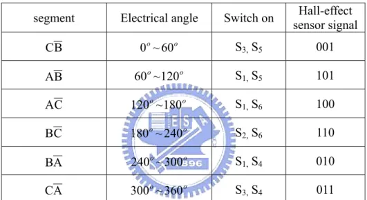
(21) Driver circuit. ia. ib Duty ratio. ic. Ha Commutation Logic. Hb. PWM control. Hc Hall-effect sensor. Fig.2.4 System schematic of a BLDC Motor by using Hall-effect sensor For example, if the Hall-effect sensors send out 001 which means the rotor position is in the segment CB , the transistors S1 and S5 in the driver circuit should be turned ON to produce the phase current pass through a to b. Then, the rotor will move to the region located in segment AB and the Hall-effect sensors will send out the three-bit signal 101. Step by step, the rotor will be rotated following the sequence of. CB , AB , AC , BC , BA , CA , and the properties related to these six segments are shown in Table.2.1. By the way, the segment AB also represents the direction of the phase current pass through a to b where ia is positive and ib is negative as shown in Fig.2.3. Additionally, the two cascaded power transistors in the driver circuit can not conduct at the same time, such as S1 must be ON while S4 is OFF, to avoid burned out. Evidently, the Hall-effect sensors are commonly used to measure the rotor. 10.
(22) position, which is important information for normally operating the BLDC motor. Unfortunately, the Hall-effect sensors have some disadvantages to face. They may increase the cost and size of the motor, or may be affected by the operating conditions, such as temperature or humidity. Therefore, the strategy of sensorless instead of the Hall-effect sensors has become more and more popular nowadays, which will be discussed in the next chapter. segment. Electrical angle. Switch on. Hall-effect sensor signal. CB. 0 o ~ 60 o. S3, S5. 001. AB. 60 o ~ 120 o. S1, S5. 101. AC. 120 o ~ 180 o. S1, S6. 100. BC. 180 o ~ 240 o. S2, S6. 110. BA. 240 o ~ 300 o. S1, S4. 010. CA. 300 o ~ 360 o. S3, S4. 011. Table 2.1 Properties related to the six segments. 11.
(23) Chapter 3 Sensorless Control for BLDC Motors From the previous chapter, in order to substitute the Hall-effect sensors located inside the motor, several sensorless control strategies have been proposed, such as back-EMF based position estimation method[10], Kalman-filter based method[4], third harmonics voltage position detection method[5], and free-wheeling diode conducting method[6]. This chapter will focus on the back-EMF based position estimation method, which will be employed in this thesis.. 3.1 Back-EMF Based Position Estimation Method In the basic BLDC motor operation, only two of three stators windings are excited at any segment and the third one is open while in the transition period with declined or rising back-EMF in Fig.2.3. Based on this appearance, the rotor position could be detected by sensing the back-EMF voltage, the so-called zero-crossing point detection, to determine the switching sequence by detecting the instant where the back-EMF in the unexcited phase crosses zero. With Y-connected stator windings and the neural voltage vn , the three terminal voltages va , vb , and vc can be expressed as. va = van + vn = Ria + L. dia + ea + vn dt. (3-1). vb = vbn + vn = Rib + L. dib + eb + vn dt. (3-2). 12.
(24) vc = vcn + vn = Ric + L. dic + ec + vn dt. (3-3). where van , vbn , and vcn are the phase voltages. Then, it can be obtained that. va + vb + vc = (van + vbn + vcn ) + 3vn. (3-4). from (3-1) to (3-3). When one phase is non-excited, its phase current will vanish and the other two phase currents are constant. For example, sections CB and BC in Fig.2.3 show that ib = −ic , eb = −ec , and ia = 0 , i.e., phase a is non-excited. In this case, the back-EMF voltage of non-excited phase a becomes. ea =. 3⎡ 1 ⎤ va − (va + vb + vc )⎥ ⎢ 2⎣ 3 ⎦. (3-5). which can be derived from (3-1) to (3-4). Similarly, the back-EMFs of non-excited phase b and non-excited phase c can be respectively obtained as. eb =. 3⎡ 1 ⎤ vb − (va + vb + vc )⎥ ⎢ 2⎣ 3 ⎦. (3-6). eb =. 3⎡ 1 ⎤ vb − (va + vb + vc )⎥ ⎢ 2⎣ 3 ⎦. (3-7). It is noticed that only the back-EMF voltage of the non-excited phase has the feature of zero-crossing, which is the basic concept of the zero-crossing point detection. As the previous example concerning non-excited phase a, the section CB and. BC. where. rotor is located are considered to obtain. The relationship between three terminal voltages and the waveform of the back-EMF ea produced from (3-5) are shown in Fig.3.1 which is matched with the Fig.2.3. Thus, when the back-EMF ea equals to zero, the position of the zero-crossing point is been detected, then the electrical angle. 13.
(25) could be in the region of 0°-60° or 180°-240°, i.e., section CB and. BC. respectively.. Furthermore, the other angles will be found with phase b and phase c in the same way. CB. Vdc. AC. AB. BC. CA. BA. va. 0 Vdc. vb. 0 Vdc vc. 0. 3 Vdc 4 0 3 − Vdc 4. ea =. 0°. 60°. 120°. 180°. 3⎡ 1 ⎤ va − (va + vb + vc )⎥ ⎢ 2⎣ 3 ⎦. 240°. 300°. 360°. Fig.3.1 Ideal three terminal voltages and the waveform of back-EMF. The system scheme in Fig.2.4 could be changed as Fig.3.2. Note that most of the existing sensorless techniques cannot be applied in the low speed range, since it is difficult to sense the zero-crossing points of back-EMF voltage from a low voltage signal. To overcome such problem, compensation algorithms have been proposed in [11], and other strategies are also proposed such as [12].. 14.
(26) Driver circuit. a. b. c. n. Duty ratio. Commutation Logic. Phase Voltage. PWM control. Zero-crossing detection. Fig.3.2 System schematic of sensorless BLDC motor drive. 3.2 Commutation Phase Shifter By the previous method, the zero-crossing signal would be produced and shown in Fig3.3, and the Hall-effect signal is also presented as reference. Compared with these two signals in Fig.3.3, the zero-crossing signal advances 30 electrical degrees. In order to produce the same commutation signal, the zero-crossing signal should be delayed 30 electrical degrees for matching the Hall-effect signal. Thus, the produced commutation signal will be correct with this sensorless method instead of Hall-effect sensor.. 15.
(27) ea −non. Zero-crossing signal. Ha. 0°. 60°. 120°. 180°. 240°. 300°. 360°. Fig.3.3 The relationship of the non-excited phase back-EMF, zero-crossing signal, and Hall-effect signal In traditional, the phase shifter with low pass filter will be affected by the rotor speed. A novel phase shifter which has been proven independent of input signal frequencies is proposed in [3], and it also can be implemented easily on a microcomputer. This frequency-independent phase shifter (FIPS) has been improved in [1] and the block diagram presented by Simulink® is shown in Fig.3.4. The variable γ which denote the decreasing increments for the counters can be set with desired degrees φ * of the phase shift and represented as. γ=. π φ*. (3-8). Thus, to produced the 30∘delayed zero-crossing signal y (k ) , γ should equal to 6 while x(k ) is the zero-crossing signal.. 16.
(28) c p (k ). xP. c n (k ) xN. Fig.3.4 Block diagram of FIPS[1]. 3.3 Start-up Strategy for BLDC Motors Since there is no or a little back-EMF to sensed when the motor standstill or at a low speed, the sensorless method based on zero-crossing detection may not be used. An additional start-up procedure should be executed first to avoid this problem. In the experiment, an open-loop start-up strategy is accomplished by providing a rotating stator field which increases gradually in frequency, and the stator field attracts the rotor field to overcome friction and inertia, then the rotor begins to rotate. Assume one of the input PWM control signal shown in Fig.3.5, and its period is changed from T1 to T4, where T1> T2> T3> T4. The final period T4 is determined in a trial-and-error way based on the specification of the motor, and the value of initial period T1 should be set a little larger. From standstill to starting, the period of the input signal attenuates with time, and the rotor will become rotating while the period equals to the final value. 17.
(29) After this start-up procedure, the motor starts rotating and the sensorless method can be used by detecting the zero-crossing points from the computed back-EMF.. T1. T2. T3. Fig.3.5 The contracted PWM control signal. 18. T4.
(30) Chapter 4 Description of DSP F2812 In the experiment of this thesis, a DSP board called ezDSPTM F2812 was utilized to realize the previous theorem. The DSP chip as a microprocessor or microcontroller in this board is TMS320F2812. It is a member of TMS320C2000 DSP generation which is a high-performance solution for demanding control applications and manufactured by TI. The generation TMS320C2000 is divided into two groups, TMS320C24x and TMS320C28x. The DSP chips, TMS320F240, TMS320LF2407A, and TMS320F2812, which belong to those two groups, are mostly used in the control applications. A roughly specification comparison of these three DSP chips is shown in Table 4.1, where the advantages of TMS320F2812 can be seen obviously due to the highest operating frequency, fastest conversion speed and 12-bit high resolution ADC module. In addition, the on-chip memory is also the largest for users to store data. Therefore, this chip is powerful in application and may be adaptive in the high-speed situation. The main purpose of using this DSP board is not only developing the algorithm inside the chip but also utilizing its useful peripherals such as ADC module and PWM waveform generation module to connect the motor plant and the driver circuit. The two modules will be introduced in the following sections.. 19.
(31) TMS320F240. TMS320LF2407A. TMS320F2812. Frequency. 20 MHz. 40 MHz. 150 MHz. CPU. 16-Bit. 16-Bit. 32-Bit. Multiply/Accumulate. 16 × 16. 16 × 16. 32 × 32. On-Chip Ram. 544 × 16. 2.5 K × 16. 18 K × 16. On-Chip Flash. 16 K × 16. 32 K × 16. 128 K ×16. ADC Resolution. 10-Bit. 10-Bit. 12-Bit. ADC Channels. 16. 16. 16. ADC Conversion time. 6.1us. 500ns. 200ns. PWM. 12-ch. 16-ch. 16-ch. Table 4.1 Specification Comparison of TMS320F240, TMS320LF2407A, and TMS320F2812 [22]. 4.1 Hardware Description The hardware description of the DSP should be divided into two parts, the DSP chip and the DSP board, and the manufacturers are different. Some problems which might occur when designing the peripheral circuit were solved by the manufacturer of the DSP board. The end user needn’t consider the problem of the compatibility when connecting to other equipments. The functional block diagram of the DSP chip is shown in Fig.4.1, and it can be roughly divided into four parts, CPU, memory, peripherals, and external interface. The external interface is not used in the experiment since no extra memory is required. To 20.
(32) enable the functions of the peripherals, some flags should be set first according to some header files released by TI for end users to define these flags. Hence, this experiment could directly give the specific command in programming instead of assembling the complicated machine code of the flags. With this functional block diagram, let’s see how to implement the motor drive procedure. First, the signals of the motor’s three-phase terminal voltages will be sent through three channels into the 12-bit ADC, which converts these analog signals into digital data and stores them in the ROM. Then, the CPU will use these digital data to execute the pre-designed process, such as the process to find the zero-crossing. Finally, the desired signals generated from the pre-designed process will be sent out through General-Purpose Input/Output (GPIO), and thus the procedure of the motor drive is realized.. 21.
(33) Fig.4.1 Functional Block Diagram [13] The layout of the DSP board ezDSPTM F2812 is shown in Fig.4.2. Socket U8 is the place where the DSP chip is installed. If the DSP chip is damaged, it can be replaced easily. Although both the JTAG interface P1 and the parallel port P3 could be used to download the DSP programs, our experiment adopts P3 only. The connectors P4, P7, and P8 are the GPIO interfaces, and the connectors P5 and P9 are the analog interfaces. Note that the input voltage of the analog interface is between 0V and 3V,. 22.
(34) thus a voltage-decaying circuit will be needed for voltage reduction. According to the previous example, the input signal must be connected to P5/P9, and the produced signal will be output by P4/P8/P7. In addition, the source voltage of this DSP board is 5V and is provided through P6. This DSP board contains six jumpers JP1, JP7, JP8, JP9, JP11, and JP12 are also shown in Fig.4.2, which are available for users to determine the functions on the DSP board. The jumper JP1 is used to set the operating mode. In this experiment, the jumper JP1 is set as microcomputer mode for the use of the software CCS. The jumpers JP7, JP8, JP11, and JP12 are used to determine what mode the DSP will use for bootloading on power up. The mode of running code from flash memory can be set by these jumpers. Users can store their program in the flash memory and load it after booting the DSP board instead of loading it again from computer. Finally, the jumper JP9 is used to enable/disable the use of the Phase Lock Loop (PLL) logic on the DSP, and the default setting “PLL Enabled” is only used in the experiment.. 23.
(35) Fig.4.2 Layout of ezDSP F2812 [14]. 4.2 Analog-to-Digital Converter (ADC) The ADC module of TMS320F2812 will be utilized in our experiments as converting the signals of the motor’s three-phase terminal voltages. The specification [15] is listed below: . 12-bit ADC core with built-in dual sample-and-hold (S/H). . Analog input: 0V to 3V. . Fast conversion time runs at 25 MHz, ADC clock, or 12.5 MSPS. . 16-channel, multiplexed inputs. . 16 result registers (individually addressable) to store conversion values. Since the input voltage is limited between 0V and 3V, a simple circuit such as shown in. 24.
(36) Fig.4.3 is used to lower down the three terminal voltages of the motor, which are analog signals and will be input to ADC module through three channels, ADCINA0, ADCINA1 and ADCINA2, shown in Fig.4.4. Actually, these analog signals Vi are converted into digital values via ADC module as. if Vi ≤ 0 V ⎧ 0 ⎪ V - ADCLO ⎪ , if 0 V <Vi < 3V Digital Value = ⎨ 4095 × i 3 ⎪ if Vi ≥ 3V ⎪⎩ 4095 where ADCLO is the reference voltage of the analog ground which located in pin18 of the port P9 shown in Fig.4.2 and 4095 is related to 12-bit resolution. The obtained digital values will be stored in the 16 Result Registers, whose addresses can be assigned in the on-chip memory. Further, re-scale the digital values within the range of 0~3 volts to match with the 16-bit ADC Result Registers such that the ADC output range will be between 0000h and FFF0h. In our experiment, the three registers, Result Reg 0, Result Reg 1 and Result Reg 2, store the converted values from ADCINA0, ADCINA1 and ADCINA2, respectively.. 25.
(37) +12V. 30KΩ. 3V 10KΩ. Fig.4.3 Voltage-divider circuit. Fig.4.4 Block Diagram of the F2812 ADC module[15] In general, programming skill in DSP code is used to simplify the initial setting and extract the signal of ADC module, so is in our experiment. It is known that the ADC control registers must be set for initializing the ADC module to determine its 26.
(38) specification such as operating mode, sampling mode, and etc. Those parameters of ADC control registers have been defined in the head files, and the users should include all these head files in their programs for parameter setting. However, using these parameters directly in our main function will make the program complicated. For simplicity, a self-defined head file is further developed by constructing a structure which define a smaller number of new parameters, each able to represent some of the parameters related to the ADC control registers. Below show part of the structure containing some new defined parameters utilize in our main function: typedef struct { int16 Ch1Out;. //Output: Channel 1 output. int16 Ch2Out;. //Output: Channel 2 output. int16 Ch3Out;. //Output: Channel 3 output. Uint16 ChSelect;. //Parameter: ADC channel selection. …… In this structure, ChSelect represent the four channels of ADC module are selected and the other Ch1Out, Ch2Out and Ch3Out respectively represent the results of the signals converted by the ADC module from channel 1, channel 2 and channel 3. To use the parameters in the structure directly, the structure is named as adc1 in main function. Therefore, if ChSelect is needed, the parameter adc1.ChSelect should be used instead. For example, in our main function, when the value of Chselect is assigned as 0x3210,. 27.
(39) it means that the channel A0, A1, A2, and A3 are selected. Then, call the ADC initial function to store the change. This will complete the initialization of the ADC module with the following code: adc1.Chselect = 0x3210; adc1.init(&adc1); By the way, the sequence of each values will affect the relationship between Result Regs and ADC channels, since the parameter Ch1Out directly point to the location of Result Reg0. In this case, the three registers of ADC, Result Reg 0, Result Reg 1 and Result Reg 2, will be assigned to respectively store the converted values from A0, A1 and A2. Result Reg 3 will store the converted value from A3. If the data of channel 1 is needed, just call adc1.Ch1Out, and the value will be obtained. For example, in the main function of our experiment, Va = adc1.Ch1Out; Vb = adc1.Ch2Out; Vc = adc1.Ch3Out; which means the digitized values of three terminal voltages va , vb , and vc can be obtained by the ADC module. Then, in the sub function, the neutral voltage vn can be computed as Vn = (Va+Vb+Vc)/3. 28.
(40) The back-EMF voltage of non-excited phase a can be computed as Ea = Vc−Vn Therefore, use if and else function, and it will be simple to judge the zero-crossing of back-EMF.. 4.3 Pulse-Width Modulation (PWM) The PWM waveforms are generated by the DSP board to control the power applied to the motor in our experiment. Both of the event manager functions, EVA and EVB, of TMS320F2812 can support eight PWM waveforms simultaneously, and only six of them in EVA are used here to generate six switching states for the 3-phase power inverters to drive the BLDC motor. Conveniently, some principal characteristics of the PWM are programmable, such as frequency, the number of outputs, dead band, asymmetric/symmetric waveform, duty cycle and transition mode. Since frequency, duty cycle and active mode are important in the controller design, each of them will be discuss below. First, the PWM frequency is obtained by dividing the CPU clock and it will affect the current of the controller as shown in Fig.4.5, where the current of the frequency in the middle range is clearly smaller than both ends. It means that the power consumes more in the low end and the high end. Hence, the PWM frequency is set at 20 KHz in our experiment to prevent unnecessary power consumption. Second,. 29.
(41) the duty cycle of the input signal controls the motor’s speed and there relationship is roughly shown in Fig.4.6. The larger the duty cycle, the faster the motor’s speed. Finally, the transition mode will influence the generating of a PWM signal. To generate a PWM signal, an appropriate timer, such as timer 1 in EVA, is needed to repeat a counting period that is the same as the PWM period. In the Fig.4.7, an asymmetric PWM waveform and timer 1 is utilized for this example. A compare register is used to hold the modulating values. The value of the compare register is constantly compared with the value of the timer counter. When the values match, a transition (from low to high, or high to low) happens on the associated output. When a second match is made between the values, or when the end of a timer period is reached, another transition (from high to low, or low to high) happens on the associated output. Therefore, active high and active low are the two transition modes in producing the PWM signal.. Fig.4.5 The relationship between the PWM frequency and the current of controller[23]. 30.
(42) input. motor’ speed. Fig.4.6 The relationship between the duty cycle of input and the motor’s speed. Fig.4.7 The two transition modes in producing the asymmetric PWM waveform[16]. The motor drive is based on the proper sequential PWM waveforms, which are used to control the six inverters shown in Fig.4.8 for driving the BLDC motor. Fig.4.9(a) shows the PWM waveforms controlling the six inverters and Fig.4.9(b) depicts one of the resultant line current of the BLDC motor matching to the currents in Fig.2.3. In the DSP code, the main purpose of generating PWM waveforms is to fulfill the proper action of the sequence in Table 4.2. The design technique is using a pointer labeled with a number in {0, 1, 2, …, 5} to represent these six states. By accumulating. 31.
(43) the number in the pointer, the desired sequence of signals is created. Notice that the PWM module has to be initialized and the same programming skill mentioned in the previous section is used again. Another self-defined head file is developed by constructing a structure which defines a less number of new parameters. The parameters such as duty ratio and transition mode can be set previously in this head file.. Fig.4.8 Three phase power inverters for a BLDC motor drive. 32.
(44) (a) S1 S4 S2 S5 S3 S6. (b) i. Fig.4.9 (a) the six PWM waveforms (b) a phase current waveform of a BLDC motor. 33.
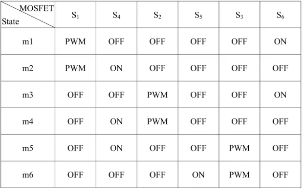
(45) MOSFET. S1. S4. S2. S5. S3. S6. m1. PWM. OFF. OFF. OFF. OFF. ON. m2. PWM. ON. OFF. OFF. OFF. OFF. m3. OFF. OFF. PWM. OFF. OFF. ON. m4. OFF. ON. PWM. OFF. OFF. OFF. m5. OFF. ON. OFF. OFF. PWM. OFF. m6. OFF. OFF. OFF. ON. PWM. OFF. State. Table 4.2 Commutation State in 3-phase BLDC Motor control. 34.
(46) Chapter 5 The DSP Programming and Hardware Implementation of Driver Circuit Based on Sensorless Method The objective of our experiment is to realize the sensorless control strategies introduced in the previous chapters. This can be separated into two parts, software and hardware. The software is programmed for the desired strategies by the tools of DSP, and the hardware is to implement amplifiers and gate drivers in some PCBs. This chapter will introduce all of the processes concerning the software and the hardware.. 5.1 The DSP Program The tools of the DSP program are SDConfig® and CCStudio®. The first one checks the connection between PC and DSP board, while the other one compiles and executes the DSP program. The views of these two programs are shown in Fig.5.1. By the way, the CCStudio® can show the change of the DSP memory data while the DSP board is executing. It is convenient to assign the number of the specific parameters in the program and easy to check which function is executing currently.. 35.
(47) (a). (b). Fig.5.1 (a) The view of SDConfig® (b) The view of CCStudio®. Since the DSP board has been introduced in Chapter 4, this section will focus on the program of the executing process, which is written in C code and divided into several parts according to their functions. Some peripheral files provided by the manufacturer must be included, where the defined parameters will be utilized in our main function. The flowchart of the program is shown in Fig.5.2 with the main 36.
(48) function on the left side and the interrupt function on the right side. The interrupt function contains some self-defined modules and executes when the change of the parameter “EnableFlag” occurs. In the main function, only the initialization of the DSP board is concerned. In F2812, all the peripherals which will be utilized should be initialized by setting the corresponding parameters. The released references such as TMS320F2812 Data Manual [17] or TMS320x281x DSP Event Manager Reference Guide [16] show how to set the parameters. At the end of the main function, an infinite loop is located. When the parameter “EnableFlag” is set to be 1, the interrupt function will be executed. In addition, the self-defined modules should be named in the main function, and the parameters in these modules can be set if needed. In the interrupt function, five self-defined modules are included to execute the specific function. The ADC_DR module drives the ADC of the DSP. It allows the ADC to convert the analog signals and store the digitized signals in the memory. The Start_UP module is utilized to drive the motor from standstill by creating the time-variant period of the PWM waveforms. This could also determine the final speed of the start-up by limiting the period of the PWM waveforms when the motor is rotating. The MOD module is utilized to check if the state is changed. Its output represents the six states of the sequence in Table 4.2 with a number in {0, 1, 2, …, 5}. 37.
(49) for normally operating the BLDC motor. When a state is going to be changed, this module will receive a trigger. Then, it will output the represented number of the next state. The PWM module drives the PWM of the DSP to produce the waveforms. It is commanded by the output of the MOD module as the introduction in Section 4.2. Finally, the Zero_Cross module is to realize the sensorless method in Chapter 3. The concept of this module is based on the ideal relationship between the terminal voltages and back-EMF shown in the Fig.5.3. The six segments are labeled as m1, m2, m3, m4, m5 and m6 matched with the Table 4.2 in order to connect with the MOD module and PWM module. Since each of them only has one zero-crossing point, it is convenient to develop six cases in the Zero_Cross module for judging the zero-crossing point. For example, in the case m1, the zero-crossing point is only occurred in the back-EMF ec, and the terminal voltage vb should be zero. Therefore, just compute the back-EMF ec by the two terminal voltages va and vc receieved from ADC and the other two back-EMFs needn’t be calculated. When the zero-crossing point is detected, a trigger will be produced. However, this trigger should not directly pass to MOD module since the reason has been introduced in Section 3.2. So, a delay function is needed to let the trigger signal delay 30 electrical degrees for matching the Hall-effect signal.. 38.
(50) c_int 0. INT. Initialize S/W modules. Save contexts and clear interrupt flags. Initialize timer, period and interrupt. Execute ADC_DR module. Initialize system and module parameters. Execute Start_UP module. loop. Execute MOD module. INT. Execute PWM module. Execute Zero_Cross module. Return. Fig.5.2 The flowchart of the DSP program. 39. Restore contexts.
(51) Vdc. m1. va. m2. m3. m4. m5. m6. 0 Vdc vb. 0 Vdc. vc. 0 Vdc ea 0 −Vdc Vdc. eb 0 −Vdc Vdc ec 0 −Vdc Fig.5.3 The relationship between terminal voltages and back-EMFs. 5.2 The Hardware Implementation of Driver Circuit To drive the BLDC motor, it is required to implement its driver circuit based on the six digital signals provided by PWM module of the DSP board, and the hardware is shown in Fig.5.4, including three parts: signal amplifier, half bridge driver unit and 40.
(52) power MOSFET. The function of signal amplifiers is to appropriately enlarge the six digital signals before passed to the half bridge driver unit since the output high voltage of the DSP board is only 3V and the required minimum input voltage of IR2110 is 9.5V. Two kinds of amplifier IC, TL072 and HA17741 with different slew rates, are chosen to design the signal amplifiers for different frequencies. The IC TL072 is capable to enlarge the 20KHz PWM signals since its high slew rate is up to 13 V/μs. The other IC HA17741 is utilized to enlarge the fully on PWM signals. In such case, all of the input signals will still be square waveforms after amplifying. The function of the half bridge unit is composed of three driver ICs, IR2110, which provide the floating channel at high side used to drive an N-channel of the power MOSFET and its high and low side referenced output channels are independent. In addition, if one of the channels detects under-voltage, the action lockout will be started to ensure sufficient gate bias for the power MOSFET. The typical connection of IR2110 to power MOSFET (IRF640N) is shown in Fig.5.5. Each IR2110 connects two power MOSFET and drive one phase of BLDC motor, and the bootstrap capacitor is utilized to charged enough voltage at the beginning for giving the floating voltage to the capacitor of power MOSFET S1. This is achieved by turning off the PWM signals in a short time at the beginning and required a waiting loop in the PWM module of the DSP program. Finally, the supply voltage is connected to Vin, and the ports, R, Y and. 41.
(53) B, are then connected to the 3 phases of the BLDC motor. With the six power MOSFET as the inverters, this completes the driver circuits matched with that of Fig.3.2.. Signal Amplifier. Half Bridge Driver Unit. Power MOSFET. Fig.5.4 The motor driver circuit. 42.
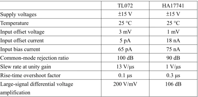
(54) Supply voltages. TL072 ±15 V. HA17741 ±15 V. Temperature. 25 °C. 25 °C. Input offset voltage. 3 mV. 1 mV. Input offset current. 5 pA. 18 nA. Input bias current. 65 pA. 75 nA. Common-mode rejection ratio. 100 dB. 90 dB. Slew rate at unity gain. 13 V/μs. 1 V/μs. 0.1 μs. 0.3 μs. 200 V/mV. 106 dB. Rise-time overshoot factor Large-signal differential voltage amplification. Table 5.1 The electrical characteristics of TL072 and HA17741 in typical condition IR2110 VBIAS. 15 V. Temperature. 25 °C. Logic “1” input voltage (min). 9.5 V. Logic “0” input voltage (max). 6.0 V. Turn-on propagation delay (typ.). 120 ns. Turn-off propagation delay (typ.). 94 ns. Shut down propagation delay (typ.). 110 ns. Turn-on rise time (typ.). 25 ns. Turn-off fall time (typ.). 17 ns. Delay matching (max). 10 ns. Vout. 10~20V Table 5.2 The electrical characteristics of IR2110 IRF640N. Drain-to-source breakdown voltage (min). 200 V. Static Drain-to-source on-resistance (max). 0.15 Ω. Gate threshold voltage (min) (max). 2.0 V 4.0 V. Drain-to-source leakage current (max). 25 μA. Rise time (typ.). 19ns. Fall time (typ.). 5.5ns Table 5.3 The electrical characteristics of IRF640N. 43.
(55) Fig.5.5 The typical connection of IR2110 to power MOSEFET [18]. 5.3 The Noise Problem during Feedback In our experiment, the noise generated by the PWM signals during feedback may cause the mistakes of the computation in the Zero_Cross module of the DSP program since the sensitivity of the ADC module of the DSP board. To overcome this problem, a hardware solution and a software solution are both considered. In the hardware solution, the low-pass filter with a voltage amplifier is shown in Fig.5.6, which is developed to eliminate the noise and reduce the terminal voltages from 0 to 3V, as the desired input of ADC module. All the scale of the components in Fig.5.6 is given in a trial-and-error way under experiment. By selecting the proper resistors and capacitors, the 20KHz PWM signals are eliminated and the 70Hz terminal voltage signals are reserved. Thus, the shape of the resulting feedback waveforms becomes trapezoid and achieves the ideal waveforms of terminal voltages shown in the Fig.3.1. By the way, 44.
(56) the practical waveforms have a little offset, but it will not affect the computation of back-EMF since the computation method introduced in section 3.1 can avoid such problem. The software solution is utilized two programming techniques in the Zero-Cross module of the DSP program. One is using moving average method to smooth the violent variation of the input signal. The ADC module of the DSP board reads 4 times of the input signals. Then, the average of these signals is computed and assigned to the corresponding variable of the program. Second is discarding the first few scans of the ADC signals when the new phase commutation occurs. When the zero crossing point appears, the trigger will be put off in a short delay to prevent the error computation. Note that the delay can not be longer than the period of the phase commutation.. Fig.5.6 The low-pass filter circuit 45.
(57) Chapter 6 Experiment Results and Analysis Since the control method and the implementation of hardware and software have been introduced in the previous chapters, the experiment results are presented in this chapter to verify those strategies and methods. The three parts of the results will be shown in the following sections: the signals dealt with the low-pass filter, the results of start-up strategy and the results of sensorless strategy.. 6.1 The Whole System of the Experiment Fig.6.1 shows the complete hardware connection of the whole system. The DSP program is compiled to the machine code by the computer, and then the machine code is downloaded to the DSP board through printer port. While the program is executing on the DSP board, the PWM signals are sent to the driver circuit for driving the BLDC motor. Then, the feedback signals dealt with the low-pass filter are passed to the ADC module of DSP board. The 3-phase BLDC motor, ALIGN BL400S, shown in Fig.6.2 is used as the experiment plant. This motor is small and has high efficiency and low power consumption with its specifications is simply listed in Table 6.1.. 46.
(58) Fig.6.1 The complete hardware connection of whole system. Fig.6.2 The BLDC motor. Input Voltage. DC 7.4 ~ 14.8 V. Dimension. Shaft = 3.17 mm 27.5×28 mm. Weight. 58 g. Max Output Power. 190 W. Pole numbers. 8. Maximum unload speed (with input voltage 11.7V). 11182 rpm. Table 6.1 The specification of the BLDC motor [24]. 47.
(59) 6.2 The Experiment results with Low-pass Filter Since the noise caused by the PWM signals may cause the computation error, a low-pass filter is utilized to deal with these terminal voltage signals. Observed by the oscilloscope, the terminal voltage signals shown in Fig.6.3 (a) are quite different after dealt with the low-pass filter. The noise contained in the original terminal voltage is eliminated by the low-pass filter, and the trapezoidal shape of the signals is retained. Through this method, the results of the three filtered terminal voltage signals shown in Fig.6.3 (b) are close to those in the Fig.5.3. Hence, it will enhance the back-EMF computation and the zero-crossing point will be detected correctly.. 48.
(60) (a). (b). Fig.6.3 (a) The comparison between the original terminal voltage signal and that dealt with the low-pass filter (b) The result of the three terminal voltage signals dealt with the low-pass filter. 49.
(61) 6.3 The Experiment results of Start-up strategy With the start-up procedure, the motor driven by the PWM signals with decaying period can rotates from standstill. In Fig.6.4, the three experiment results show the appearance of the attenuate PWM signals produced by the DSP board. The duration of the start-up procedure may influence the rotor rotation since the supply voltages for motors in different size are not the same. Hence, it is important to choose the proper duration by setting the value of parameters defined in DSP program. In the experiment, the duration is almost 2 sec. when the duty ratio of the PWM signals is 0.2, but it may be less than 1 sec. while the duty ratio is larger than 0.5. This is because the larger the duty ratio is, the more the excited current will be. Finally, the motor is starting when the period is fixed in the final value and the sensorless procedure will executed immediately to keep the rotation or change the motor speed. The terminal voltages measured by oscilloscope are shown in Fig.6.5 when the start-up procedure is ended.. 50.
(62) Fig.6.4 The appearance of the attenuate PWM. 51.
(63) Fig.6.5 The terminal voltages at the end of start-up procedure. 6.4 The Experiment results of Sensorless strategy In order to do the sensorless procedure, the digitized signals converted by the ADC module should be checked if they are corresponding with the input signals. Fig.6.6 shows that the ADC module absolutely converts the input signals into digital signals. Then, the back-EMFs, computed by the Zero-Cross module of DSP program with the equations (3-5)–(3-7), are shown in Fig.6.7. The relationship between the digitized signals and the back-EMFs is shown in Fig.6.8. These experiment results and Fig.5.3 are matched and the zero-crossing point can be well detected since the error of computation is reduced. When the zero-crossing point is detected, the trigger determined in the Zero_Cross module of DSP program is delayed 30 electrical degrees to produce the correct PWM signals, which have been introduced in Section 3.2, and. 52.
(64) the relationship between the delayed trigger and the back-EMFs is shown in Fig.6.9. After the start-up procedure, the sensorless procedure is executed immediately to keep the rotation and the motor speed can be regulated in this process. From Fig.6.10 to Fig.6.13, the experiment results are shown when the motor is rotating with the different PWM duty ratio.. Fig.6.6 The results of digitized input signals by ADC module. 53.
(65) Fig.6.7 The computed back-EMFs. Fig.6.8 The relationship between the digitized input signals and the back-EMFs. 54.
(66) Fig.6.9 The appearance of the delayed trigger with the digitalized input signal and the back-EMF. 55.
(67) (a). (b). Duty ratio =0.2 (c). Fig.6.10 (a) The PWM signals (duty ratio = 0.2) (b) The enlarged PWM signals (c) The terminal voltages. 56.
(68) (a). (b). Duty ratio =0.37 (c). Fig.6.11 (a) The PWM signals (duty ratio = 0.37) (b) The enlarged PWM signals (c) The terminal voltages. 57.
(69) (a). (b). Duty ratio =0.8 (c). Fig.6.12 (a) The PWM signals (duty ratio = 0.8) (b) The enlarged PWM signals (c) The terminal voltages. 58.
(70) (a). Duty ratio =1 (b). Fig.6.13 (a) The PWM signals (duty ratio = 1) (c) The terminal voltages. 59.
(71) Chapter 7 Conclusions The main purpose is to achieve the sensorless driving technology and implement it to steer the BLDC motor from standstill to a fixed speed. In addition, the motor speed can be regulated by changing the duty-ratio of PWM signals. During the operation, the start-up procedure is executed first until the period of the output signals matches to the desired value, and then the sensorless procedure is started immediately. This completes the rotation of the BLDC motor from standstill to a fixed speed. The duration of the start-up procedure, tuned in the DSP program, may influence the rotor rotation since the supply voltages for motors in different size are not the same. Usually, big motors need more power, which means the start-up duration should set a little longer for larger excitation current. On the other hand, the R/C motor used in the thesis is small and need less power, so the duration of the start-up procedure could be shortened. The feedback technology is utilized to grab the 3-phase terminal voltages of the motor for sensorless control strategy processing, but the ADC module of the DSP board is sensitive and may record the noise caused by PWM signals. The computation error may occur correspondingly, so a low-pass filter designed by trial-and-error way and some techniques applied in the DSP program are used to avoid such problem. As a. 60.
(72) result, the zero-crossing point will be well detected, and the produced PWM signals may not be delayed to influence the rotation. By the way, if the low-pass filter is not used, the motor may fail to rotate or rotates unsmoothly. The whole system is established to achieve the BLDC motor drive, and all of the strategies is implemented in the DSP program and executed on the DSP board. In the program, all the functions of the strategies are divided into several modules connected by the internal signal parameters. In the future, a PI or PD controller may be developed as a module of the program to connect with the corresponding internal signals such as ADC memories or PWM output control to achieve the goal. Additionally, the starting and the duty ratio changing instructions are commanded directly by the computer in the real-time mode since it is convenient to observe the change of the memory. These instructions may be given by other input signals from external voltages through the interfaces of the DSP board as the future work.. 61.
(73) Reference [1]. K. Y. Cheng and Y. Y. Tzou, “Design of a Sensorless Commutation IC for BLDC Motors,” IEEE Transactions on Power Electronics, vol.18, no.6, pp.1365-1375, November 2003.. [2]. J. Shao, D. Nolan, and T. Hopkins, “Improved direct back EMF detection for sensorless brushless DC (BLDC) motor drives,” in Proc. IEEE-APEC Conf., pp.300-305, 2003.. [3]. D. H. Jung and I. J. Ha, “Low-cost sensorless control of brushless DC motors using frequency-independent phase shifter,” IEEE Transactions on Power Electronics, vol.15, no.4, pp.744-752, July 2000.. [4]. B. Terzic and M. Mohan, “Design and Implementation of the Extended Kalman Filter for the Speed and Rotor Position Estimation of Brushless DC Motor,” IEEE Transactions on Industrial Electronics, vol.48, no.6, pp. 1065-1073, December 2001.. [5]. J. C. Moreira, “Indirect Sensing for Rotor Flux Position of Permanent Magnet AC Motors Operating Over a Wide Speed Range,” IEEE Transactions on Industry Applications, vol.32, no.6, pp.1394-1401, November 1996.. [6]. S. Ogasawara and H. Akagi, “An approach to position sensorless drive for brushless dc motors,” IEEE Tran. Industry Applications, vol. 27, no. 5, pp. 62.
(74) 928-933, Sep. /Oct. 1991. [7]. K. Iizuka, H. Uzuhashi, M. Kano, T. Endo, K. Mohri, “Microcomputer control for sensorless bruchless motor,” IEEE Trans. Ind. Applicat., vol, pp.595-601, May/June 1985.. [8]. T. H. Kim and M. Ehsani, “Sensorless Control of the BLDC Motors From Nero-Zero to High Speeds,” IEEE Trans. Power Electronics, vol. 19, no. 6, pp.1635-1644, Nov. 2004.. [9]. P. Pillay and R. Krishnan, “Modeling, Simulation, and Analysis of Permanent-Magnet Motor Drives, Part II: The Brushless DC Motor Drive,” IEEE Trans. Industry Applications, vol. 25, no. 2, pp.274-279, Mar. 1989.. [10] J. Shao and D. Nolan, “Further Improvement of Direct Back EMF Detection for Sensorless Brushless DC (BLDC) Motor Drives,” in Applied Power Electronics Conference and Exposition, IEEE-APEC, vol. 2, pp.933-937, 2005 [11] G. H. Jang, J. H. Park, and J. H. Chang, “Position detection and start-up algorithm of a rotor in a sensorless BLDC motor utilizing inductance variation,” IEEE Proc. Power Applications, vol. 149, no. 2, pp.137-142, Mar. 2002. [12] Y. Kang, S. B. Lee, and J. Yoo, “A Microcontroller Embedded AD Converter based Low Cost Sensorless Technique for Brushless DC Motor Drives,” in Industry Applications Conference, Fourtieth IAS Annual Meeting, vol. 3,. 63.
(75) pp.2176-2181, 2005. [13] “TMS320F2812 Digital Signal Processor Data Manual,” SGUS053, Taxes Instruments, Dec. 2004. [14] “eZdsp F2812 Technical Reference,”, 506265-0001 Rev. C, Spectrum Digital, Sep. 2002. [15] “TMS320x281x Analog-to-Digital Converter (ADC) Reference Guide,” spru060d Rev. D, Taxes Instruments, Jul. 2005. [16] “TMS320x281x Event Manager (EV) Reference Guide,” spru065d Rev. D, Taxes Instruments, Aug. 2006. [17] “TMS320F2810,. TMS320F2811,. TMS320F2812,. TMS320C2810,. TMS320C2811, TMS320C2812 Digital Signal Processors,” SPRS174N, Taxes Instruments, May. 2006. [18] IR2110/2113(S) Data Sheet No.PD60147-O from International Rectifier Company. [19] 程思穎, 直流無刷馬達無感測驅動技術之實現 , 國立交通大學電機與控制 工程學系, 碩士論文, 2006.. [20] 陳志成, 無轉軸偵測元件之無刷馬達驅動系統研製, 國立中央大學電機工 程學系, 碩士論文, 2001.. [21] 林翰宏, 無刷直流馬達之分析與無感測器驅動之建模, 國立交通大學電機. 64.
(76) 與控制工程學系, 碩士論文, 2004.. [22] http://www.ti.com/ [23] http://www.seattlerobotics.org/encoder/200011/pwm.html [24] http://www.align.com.tw/. 65.
(77)
數據
![Table 6.1 The specification of the BLDC motor [24]Fig.6.2 The BLDC motor](https://thumb-ap.123doks.com/thumbv2/9libinfo/8102545.165246/58.892.132.759.120.365/table-specification-bldc-motor-fig-bldc-motor.webp)
相關文件
See Chapter 5, Interrupt and Exception Handling, in the IA-32 Intel Architecture Software Developer’s Manual, Volume 3, for a detailed description of the processor’s mechanism
Before the frame start specified in PMC_RSP, the MS shall transmit PMC_REQ in response to receipt of an PMC_RSP from the BS directing a change to uplink power
Starting from a discussion on this chapter, Jay a nanda proceeds to explain 22 kinds of mental initiation for the pursuit of enlightenment... The first chapter of Madhyamak a vat a
Thus, for example, the sample mean may be regarded as the mean of the order statistics, and the sample pth quantile may be expressed as.. ξ ˆ
Al atoms are larger than N atoms because as you trace the path between N and Al on the periodic table, you move down a column (atomic size increases) and then to the left across
Now, nearly all of the current flows through wire S since it has a much lower resistance than the light bulb. The light bulb does not glow because the current flowing through it
We have been promoting STEM education among schools in a holistic and coherent manner, with strategies that embrace renewing the curricula of the Science,
Numerical results are reported for some convex second-order cone programs (SOCPs) by solving the unconstrained minimization reformulation of the KKT optimality conditions,
