Nano-structured Metal-Oxide-Semiconductor Devices for Efficient
Band-edge Electroluminescence
Peng-Fei Chung', Ting-Wien Si?,
Ching-Fuh
Lina,*, Miin-Jang Chenc, and Wei-Fang Su'
bGraduate
Institute of Electro-Optical Engineering, National Taiwan University, Taiwan, R.O.C.
aalso
with Graduate Institute of Electronics Engineering and Dept. of Electrical Engineering,
National Taiwan University, Taiwan, R.O.C.
C
Institute
ofApplied Science and Engineering Research, Academia Sinica, Taiwan, R.O.C.
d Institute of Materials Science and Engineering, National Taiwan University, Taiwan, R.O.C.
Email: [email protected]
Abstract
We report that electroluminescence (EL) at Si bandgap energy is significantly enhanced from the nano-structured metal-oxide-semiconductor (MOS) devices on silicon. The nano-structure is constructed by inserting Si02 nanoparticles with the size of 12 nm in the oxide layer. The measured EL efficiency of the nano-structured MOS devices is enhanced to be near iO, which exceeds the limitation imposed by the indirect bandgap nature of silicon. We also observed the nearly lasing behaviors such as the threshold and resonance modes in the EL characteristics. The enhanced EL efficiency is attributed to simultaneous localization of electrons and holes to form exciton by nano-structure. This causes the process of the phonon-assisted radiative recombination of electron-hole pair more like two-particle (exciton-phonon) collision than three-particle (electron-hole-phonon) collision.
Keywards : Silicon, MOS, electroluminescence. nanoparticle
1. Introduction
Because of the dominance of silicon in ultra-large-scale-integration (ULSI) circuits, there has been a strong desire to realize monolithic integration of microelectronics and optoelectronics on a single silicon chip. However, silicon has limited applications in area of optoelectronics due to its indirect bandgap characteristics that make it hardly emit light. In order to convert silicon to a light-emitting material, many efforts had been tried before, including porous silicon, nanocrystalline Si, Si/Ge alloy, and Erbium doping of Si, and so on 113• However,this luminescence originates from either the defect-related mechanisms or band-structure modification. The fabrication processes are complicated and not commonly used in current ULSI technology, leading to the difficulty of commercial applications.
Recently, MOS structures on silicon with the ultrathin oxide grown by the well-controlled rapid thermal oxidation (RTO) had also been discovered to exhibit significant EL at silicon bandgap energy at room temperature. Becausethe structure and processing steps are compatible with current ULSI circuits, it shows the promise to realize monolithically integrated electronics and optoelectronics on a single chip based on silicon. However, the EL efficiency is only in the order of lO from the conventional MOS structures with RTO grown oxide without special treatment 13,14 Inthis paper, we demonstrate that Si02 nanoparticles with the size of 1 2 nm in the oxide layer creates the nano-structure MOS devices. The nano-structure could enhance EL efficiency at silicon bandgap energy from MOS structures for orders of magnitudes. The measured EL efficiency from the nanoparticle-modified MOS devices is enhanced to near lO, compared to the 10
8
efficiencyfrom conventional MOS structures without using Si02 nanoparticles. In addition, the nanoparticle-modified
MOS devices exhibit nearly lasing actions such as the threshold behavior and resonance modes. As a result, the efficient light-emitting MOS devices with nano-structure show promise to achieve the practical on-chip light source for optical interconnection and silicon-based optoelectronics integrated circuits (OEIC).
+
2. Device Fabrication
The processing steps and device structures for nano-structured MOS are very simple. The Si02 nanoparticles were used in the insulation layer ofthe MOS structure to create nano-structures. The processing steps are described as follows. The (100) Si wafers used in the experiment were n-type with the resistivity of 1-10 Q-cm. The wafers were first cleaned with standard processing techniques and the native oxide on the silicon wafer was removed by buffer-oxide-etchant (BOE). The cleaning process helps nanoparticles spread out on the silicon surface. Otherwise, the 5i02 nanoparticles cannot be smoothly and uniformly deposited. Afterwards, diluted solution with 5i02 nanoparticles were spun onto the wafer. The size of nanoparticles is about 12 nm in diameter, which is held in isopropyl alcohol solution. The original solution with 30% (by weight) 5i02 nanoparticles, IPA-ST-S it was diluted by adding several times of the isopropyl alcohol solvent in volume. The use ofproper solution is critical. Ifwater solution is used, the surface tension ofwater will cause the nanoparticles to fly off the Si surface together with the water. Afterwards, the sample was dried in the oven at the temperature 88'-90°C for about 1 minute to remove the isopropyl alcohol solvent. Several dilution ratios and spin speeds have been experimented. Depending on the dilution ratio and the spin speed, the thickness of the insulation layer ranges from 500 nm to 2000 nm. The thickness ofoxide is measured by ellipsometry. The SEM photo (field-emission type) ofthe spun-on 5i02 nanoparticles is shown in Fig. 1 .Thespun-on 5i02 nanoparticles form an insulation layer with grainy structures with a feature size of 12 nm, determined by the nanoparticle size. Aluminium metal was deposited on the nanoparticles using thermal evaporation to form the gate electrode in the MOS structure. Silver paint is then applied on top ofit to hold a gold wire for electrical contact. A thick layer ofAl is also evaporated onto the back side ofthe Si to form another electrical contact. A schematic ofthe device is shown in Fig. 2.
100 nrn
Fig. I SEM photo of Si02 nanoparticles spun on the Si surface.
Al
cY'cTyc)cD
NanoparticleSi
v__
Al
3. I-V Characteristics, Electroluminescence Spectra and Efficiency
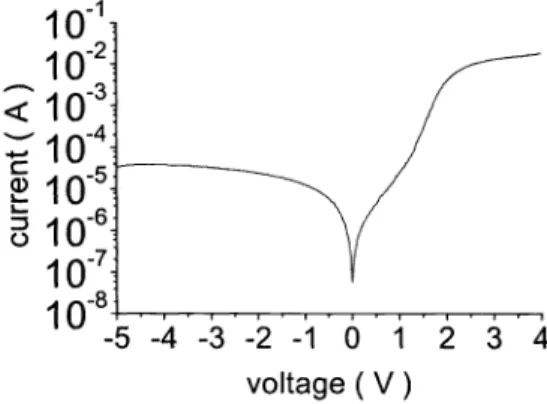
Because the spun Si02 nanoparticles are not tightly packed, there are lots of hollow spaces between those particles. During evaporation, the Al metal could get into those hollow spaces. Therefore, Al metal could be very close to the Si surface. In some areas, the insulation layer is thin enough to allow carriers tunneling through. The measured I- V (current-voltage) characteristics are shown in Fig. 3 The I- V curve shows the rectifying characteristics. When the gate is biased at negative voltage, an inversion layer ofthe holes is formed at Si/Si02 interface, as shown in Fig.4(a). As long as the holes in the inversion layer are generated, they tunnel away to the metal gate and the inversion layer is always kept at the onset of the inversion region, instead of the strong inversion. The reverse-biased current is limited by the generation rate of the holes through the Si/Si02 interface state and so is much smaller than the forward biased current.
Note that there is a kink in the I- V characteristics at the forward bias about 1 V in Fig.3, which implies two different current tunneling mechanisms. I5,6
At
applied gate voltage smaller than 0.5 V, the current is composed of the electrons tunneling from the Si conduction band and from the Si/5i02 interface state to metal gate. (see Fig.4 (b)). When the gate voltage is larger than 1 V, lots of majority electrons are accumulated at the silicon surface, as shown in Fig.4 (c). The tunneling probability also increases rapidly with the gate voltage due to the reduced effective barrier height. These result in significant tunneling current. As indicated in Fig.4(c), the holes tunneling from the metal gate to the Si valence band also contribute to the total current.0—•
Ill/Ill
I
I
<I
voltage(V)
Fig. 3 1- V characteristics of the nano-structured MOS devices.
Fig.4 Schematic band diagram of of the nano-structured MOS devices.
-4 -3 -2 -1
0
12 3 4
metal Si02 metal
Si02 n-Si metal Si02 n-Si
n-Si
(a)
leakage 1111111 EF (b) (c)When significant current tunnels through the insulation layer, EL is clearly observed through an JR-viewer even with a very low injection current density <
I
A/cm2. The diode is operated at room temperature under continuous wave operation without cooling. Because ofthe different barrier heights between the electrons (3.1eV) and holes ('-5.6eV), the electron tunneling current is much larger than the hole tunneling current. As shown in Fig.4 (c), EL was still observed even though the electron tunneling current acts as the leakage current for radiative recombination.The EL spectrum from the nano-structured MOS devices is shown in Fig.5. The spectrum was measured using an InGaAs detector placed at the exit of the monochromator (CVI, CM1 10). The peak of spectrum is slightly below the bandgap energy of crystalline silicon at room temperature due to the participation of optical phonon in the radiative recombination.9 The spectrum could be explained by models including optical phonon, interface roughness, and localized
carriers. 3,14,17-19Theemission ofTO phonon with energy 57.8 meV is known as the dominate mechanism for momentum
conservation for radiative recombination and so contributes to the main peak of the emission
tru'9 The
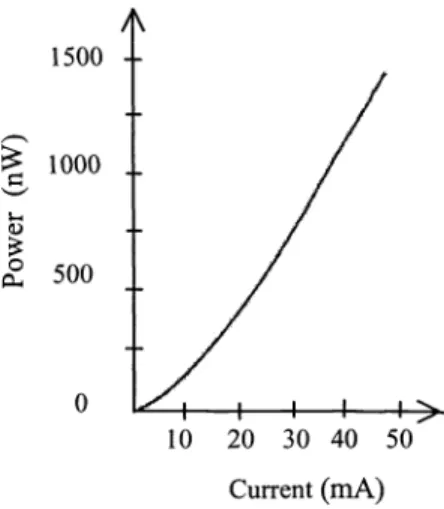
long-wavelength tail in the Fig.5 is due to the two-phonon process with the phonon energy 57.8+64.5 meV (TO+ Or), emission of a momentum-conserving TO phonon and a zone center (Or) phonon. 'Thecalculated luminescent lineshape of the main TO peak and two-phonon signal is demonstrated in Fig. 6. 'Becausethe evaporated Al atoms mostly get into the hollow space of the nanoparticles, they can hardly conduct current laterally. As a result, the silver paint is the main conductive material for current flow, so EL mainly takes places under the silver paint. Therefore, most of light is blocked by the thick silver paint. If only the light emitted from the periphery ofthis pad is taken into account, the measured slope efficiencies ofEL are all more than 1 x 10⁶ at the injection current density of 1.67 A/cm2. The best efficiency could be 4 x iO. Fig. 7 shows the L-I curve of the efficient light emission at the Si bandgap energy. The light emitted to the edge of the device is also measured. The total optical power emitted from the four edges is approximately equal to that measured from the top of the pad, so the total measured efficiency could be near iO. There is still some portion of light totally blocked by the pad of silver paint, so the actual efficiency should be better than lO. In addition, all of the L-I characteristics measured at room temperature show a
suprelinear increase with the injection current. Thus more efficiency is expected as the current density increases. The
1.o
Co
cDV:
0.0!
0.9
1.0
photon energy (eV)
Fig.5 The EL spectrum of the nano-structured MOS devices
1.0
0.8
- 0.6
>
0.4
a)0.0
0.9
1.0
1.1 1.2photon energy (eV)
1.3
measured efficiencies from nano-structured MOS devices are orders of magnitudes stronger than previous reports on conventional MOS structures without nanoparticles. 13,14
1500 1000 a) 500 0 - I 10 20 30 40 50 Current
(mA)
Fig.7 The L-I curve ofthe efficient light emission from nano-structured MOS device.
4. Threshold Behavior and Resonance Modes
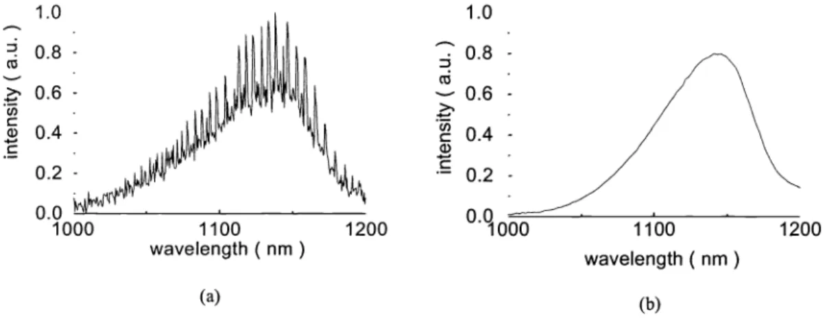
With the enhanced EL efficiency from the nano-structured MOS decives, one of the devices exhabits the near lasing behavior. Figure 8(a) shows a sudden increase of the output power after the threshold current ( 12mA) in the measured L-I (optical power-current) characteristics. The corresponding spectrum at 50 mA is shown in Fig. 9(a). Although the resolution of our monochromator (CVI, CM1 10) is not able to completely resolve each Fabry-Perot mode of the MOS device, some of the resonance modes are still observed in Fig. 9(a). The L-I curve of another device without threshold is shown in curve (b) in Fig. 8 as a comparsion. Its output power shows only a graduate increase with the injection current. Figure 9(b) is the spectrum corresponding to Fig. 8(b). No resonance modes are observed for the devices without the threshold behavior. The possible reason for the near lasing behaviors will be discussed later.
400 300
1
a) 2000
1000
Current (mA)
Fig. 8 Room-temperature L-I curves: (a) the device with threshold. (b) the device without threshold.
(a)
(b)
1.0 1.0 0.8
-c
.
0.6 -U) a)0.4
0.2-0.0
1000 1200 1200 wavelength (nm)
(a) (b) Fig. 9 EL spectrum (a) with resonance modes, corresponding to L-I curve in Fig. 7(a)(b) without resonance modes, corresponding to L-I curve in Fig. 7 (b)
5. Discussions
Possible reasons for the efficient EL from the nano-structured MOS devices at room temperature are discussed as follows. The main reason for inefficient light emission from indirect-bandgap semiconductors is attrributed to the low radiative recombination rate of electrons and holes, which is in the order of 104/sec. In comparison, the typical
electron-hole radiative recombination rate in the direct-bandgap semiconductor such as GaAs and InP is in the order of 1 09/sec. On the other hand, the transition rate of electrons from the conduction band to the valence band via the non-radiative
recombination centers is usually in the order of iO /sec. For direct-bandgap materials, because the radiative
recombination rate is much larger than the non-radiative one, light emission is quite easy. In contrast, the radiative recombination rate is only one-tenth of the non-radiative one for indirect-bandgap semiconductors. Thus light emission is inefficient in indirect-bandgap materials because the non-radiative recombination is the dominant process.
For the state-of-the-art ULSI technology, the non-radiative transition rate is in the order of 105/sec in silicon, which is larger than the radaitive recombination rate for only about one order of magnitude. If some mechanism is provided to
increase the radiative recombination rate and/or decrease the non-radiative recombination rate, the radiative
recombination might dominate over the nonradiative recombination in siliocn. Then efficient light emission from indirect-bandgap materials becomes possible.
Because of the indirect bandgap of cryatalline silicon, some mechanisms are required for momentum conservation in the radiative recombination. In addition to the participation of phonons, several mechanisms had been proposed to possibly increase radiative recombination. 'The carrier scattering by Si/Si02 interface roughness was shown to be important to provide some momentum to compensate the momentum-mismatch between the electrons and holes in the
k-space. 14,18Anothermechanism is the spatial localization ofcarriers. The localized carriers cause the spreading of carrier momentum in the recopical space due to the uncertainty principle and so relax the momentum mismatch between electrons and holes. In addition, it also leads to the easy formation of excitons, so phonons can more easily involve in the electron-hole radiative recombination. If an electron and a hole are already bound together spatially to form an exciton, radiative recombination involves only two particles, an exciton (or electron-hole pair) and a phonon. In constract, if the radiative recombination involves three particles, an electron, a hole, and a phonon, the probability for the three particles to meet together is very low. Therefore, the two-particle collision has a much higher probability than the three-particle collision. Therefore, radiative recombination is greatly enhanced.
The nanoparticles inserted in the insulation layer could enhance the spatial localization ofcarriers. The nanoparticles cause the thickness of the insulation layer between the metal gate and silicon to be nonuniform and results in the following
Co
0.6
- >-Cl) Co0.2
-1100
wavelength
(nm)
1100two effects.First, when the positive gate voltage is applied, the thin-oxide region has a stronger voltage gradient than the thick-oxide region. Thus the band bending of silicon near the thin oxide region is more severe than the thick oxide region, resulting in three-dimensional potential wells for carrier confinement in the accumulation layer near the Si/Si02 interface. Fig. 10 shows a two-dimensional (x-z) schematic diagram of the band structure for devices on n-type silicon under positive gate volatge. The behavior along the y-axis is similar to that along the x-axis. Second, in the region with the thin oxide, more carriers tunnel to Si through the thin oxide layer than through the thick oxide layer. This equivalently provides two-dimensional confinement for the tunneled carriers. Therefore, electrons and holes coincidentally have the similar spatial confinement near the Si/Si02 interface. The spatial localization of electrons and holes in the same region possibly helps the formation of excitons. The probability of radiative recombination is then enhanced because the process is now more like two-particle (phonon vs. electron-hole pair) collision than the three-particle (electron, hole, phonon) collision. In this way, the indirect-bandgap obstacle is overcome to make the indirect-bandgap material behave similarly to the direct-bandgap semiconductors.
Because the nanoparticles are only applied on the surface of silicon substrate, they cause no significant influence on the structure of silicon crystal, leading to the emission remained at Si bandgap energy. Furthermore, Si02 nanoparticles are stable, not chemically influenced by the standard semiconductor processing techniques. Therefore their related processing steps are compatible with the standard ULSI technology.
The nearly lasing behavior takes place probably because the minimal non-radiative recombination states and the optimal enhancement of radiative recombination by the Si02 nanoparticles coincidentally occur at the same location of thesiliocn substrate. Therefore, a significant gain could occur in the crystalline silicon. Because silicon is an indirect
bandgap material, its absorption is not signifivant at the bandgap energy as compared to the direct-bandgap
semiconductors. Thus the gain possibly surpasses the absorption loss in the region without injection current, resulting in the nearly lasing actions.
Al
Fig. I 0 Two-dimensional (x-z) schematic of the band structure for devices made on n-type siliocn under positive gate voltage. The behavior along the y-axis is similar to that along the x-axis. The dashed arrows point to the regions with the thin oxide, where more holes tunnel to silicon.
6. Summary
In summary, the EL efficiency at Si bandgap energy is significant enhanced from nano-structured MOS devices at room temperature. The measured EL efficiency is near iO, which breaks the limitation ofindirectbandgap ofthe silicon. The nanoparticles cause the thickness of the insulation layer in MOS devices between the metal gate and silicon to be nonuniform and result in the simultaneous spatial localization of electrons and holes. This makes the electron-hole radiative recombination more like two-particle collision than three-particle collision. Therefore the probability of radiative recombination increases. The nearly lasing actions like the threshold behavior and resonance modes are also observed. The efficient nano-structured MOS devices shows promise to achieve the monolithically integration of microelectronics and optoelectronics on a single silicon chip.
energy
Ec
Ef
Si Si02
ACKNOWLEDGEMENTS
The authors acknowledge the support from National Science Council, ROC under the contract NSC9O-2622-L-002-002.
References
1. David J. Lockwood, Light Emission in Silicon From Physics to Devices, Academic Press, 1998 2. Robert Hull and John C, Bean, Germanium Silicon: Physics and Materials,Academic Press, 1999.
3 . L.T. Canham, "Siliconquantum wire array fabrication by electrochemical and chemical dissolution of wafers" , AppI.Phys. Lett. 57,pp.1046-1046, 1990.
4. S. Lazarouk, P. Jaguiro, S. Katsouba, G. Masini, S. La Monica, G. Maiello, and F. Ferrari, "Stableelectroluminescence from reverse biased n-type porous silicon—aluminum Schottkyjunction device", Appl. Phys. Lett. 68, pp.2108-2110, 1996.
5. 5. Schuppler, S. L. Friedman, M. A. Marcus, D. L. Adler, Y.-H. Xie, F. M. Ross, Y. J. Chabal, 1. D. Harris, L. E. Brus, W. L. Brown, E. E. Chaban, P. F. Szajowski, S. B. Christman, and P. H. Citrin, "Size,shape, and composition ofluminescent species in oxidized Si nanocrystals and H-passivated porous Si", Phys. Rev. B 52, pp.4910-4925, 1995.
6. D. B. Geohegan, A. A. Puretzky, G. Duscher, and S. J. Pennycook, "Photoluminescence from gas-suspended SiO nanoparticles synthesized by laser ablation", Appl. Phys. Lett. 73, pp.438-440, 1998.
7. L. S. Liao, X.-M. Bao, X.-Q. Zheng, N-S. Li, andN.-B. Min,"Blueluminescence from Si-imp1anted Si02 films thermally grown on crystalline silicon", AppI. Phys. Lett. 68, pp.850-852, 1996.
8. M. Matsuoka and S. Tohno, "Electroluminescence oferbium-doped silicon films as grown by ion beam epitaxy" , Appl. Phys. Lett.
7l,pp.96-98, 1997.
9. D. R. Baigent, R. N. Marks, N. C. Greenham, R. H. Friend, S. C. Moratti, and A. B. Holmes, "Conjugated polymer light-emitting diodes on silicon substrates",Appl. Phys. Lett. 65,pp.2636-2638, 1994.
10. M. Garter, J. Scofield, R. Birkhahn, and A. J. Stecki, "Visible and infrared rare-earth-activated electroluminescence from indium tin oxide Schottky diodes to GaN:Er on Si", Appl. Phys. Lett. 74, pp.182-184, 1999.
I 1 . A.Loni, A. J. Simons, T. I. Cox, P. D. J. Calcott, L. T. Canham, "Electroluminescent porous silicon device with an external quantum efficiency greater than 0.1% under CW operation", Electron. Lett., 31, pp.1288-1289 ,1995
12. 5. Coffa, F. Priolo, G. Franzo, A. Polman, S. Libertino, M. Saggio, and A. Camera, "Materials issues and device performances for light emitting Er-implanted Si ",NuclearInstruments and Methods in Physics Research B, 106, pp.386-392, 1995
13. Ching-Fuh Lin, C. W. Liu, Miin-Jang Chen M. H. Lee, and I. C. Lin, "Electroluminescence at Si Bandgap Energy Based on Metal-Oxide-Silicon Structures," J. AppI. Phys., 97, pp8793-8795, 2000.
14. C. W. Liu, M. H. Lee, Miin-Jang Chen, I. C. Lin, and Ching-Fuh Lin, "Room-Temperature electroluminescence from electron-hole plasmas in the metal oxide silicon tunneling diodes," Appi. Phys. Lett., 76, pp.1516-iSiS, 2000.
.1_i C. W. Liu, W. T. Liu, M. H. Lee, W. S. Kuo, and B. C. Hsu, "A novel photodetector using MOS tunneling structures", IEEE Electron Device Lett. 21, pp.307-309, 2000.
16. A. Ghetti, E. Sangiorgi, J. Bude, T. W. Sorsch, and G. Weber, "Low voltage tunneling in ultra-thin oxides: a monitor for interface states and degradation", Tech. Dig. Int. Electron Devices Meet. Pp.731-734, 1999.
17. C. W. Liu, M-J Chen, I. C. Lin, M. H. Lee, and C-F Lin, "Temperature dependence of the electron-hole-plasma
electroluminescence from the metal-oxide-silicon tunneling diodes," Appl. Phys, Lett. 77, pp.1111-1113, 2000.
18. C. W. Liu ,M.H. Lee, M. J. Chen, C-F Lin, and M. Y. Chern ,"Roughness-enhancedelectroluminescence from
metal-oxide-silicon tunneling diodes," IEEE Electron Device Lett. ,vol. 21(6), pp.601-603, 2000.
19. Miin-Jang Chen, Eih-Zhe Liang, Shu-Wei Chang, and Ching-Fuh Lin, "Model for band-edge electroluminescence from metal-oxide-semiconductor silicon tunneling diodes," .1. App!. Phys., 90, pp.789-793, 2001.