Optimized Design of a Floating-Point Matrix
Multiplier
Lan-Chau Yang
Department of Computer Science and Information Engineering National Chi Nan University
Puli, Nantou Hsien, 54561 Taiwan Email: [email protected]
Dyi-Rong Duh
Department of Computer Science and Information Engineering National Chi Nan University
Puli, Nantou Hsien, 54561 Taiwan Email: [email protected]
Abstract―Floating-point matrix multiplications are widely used in many complex scientific computations. To accelerate such enormous computing, a large number of researches are investigating a more efficient floating-point matrix multiplier. Matrix multiplication consists of many multiplications and accumulations. Both of them sum up two vectors to one in the final stage. By using a CLA could achieve the final addition. The CLA is faster than a traditional CPA in computation time. However, it still consumes much time and many hardware costs. This work proposes an efficient design of a floating-point matrix multiplier. In the process of accumulating products, we reserve the two vectors generated from multiplication arithmetic and take advantage of CSAs to accumulate products. Finally, the carry and sum vectors generated from CSAs will be summed through a CLA. Thus one result of matrix multiplication is obtained. On the other hand, this design of floating-point matrix multiplier also includes the scalable concept. The multiplier and adder are divided into two modules. According to the demands on delay and cost, a developer can make a decision and accomplish an optimized design of a floating-point matrix multiplier.
Index Terms―Matrix multiplication; floating-point number; floating-point arithmetic; merged arithmetic; partial product matrix reduction.
I. INTRODUCTION
Since many scientific applications involve performing complex floating-point computations, a large number of researches on improving the performance of floating-point operations have been proposed [2], [7], [15]. The amount of representable bits of a floating-point number is finite. Fast rounding operation is necessary to deal with redundant bits generated in floating-point operations [12], [13], [14]. Furthermore, the matrix multiplication is widely used within these scientific
computations. The basis of matrix multiplication, inner product, consists of multiplication and accumulation. Thus the execution time of multiplication and addition is concerned.
In 1969, Strassen proposed an algorithm computing the inner product of two square matrices of order n, and the time complexity is
approximately O(n2.8), in contrast that the
traditional one takes O(n3) [16]. Nowadays, there
are more and more components can be made on a smaller chip. People intend to resolve the matrix multiplication in multiple processors. In [9], Huang
and Duh proposed architecture with n2 PEs
(Processing Element) to compute the matrix multiplication ordered by n. The time delay for data transfer does not exist since it using data sharing on the bus. As a result, the computational complexity is O(n) on their proposed structure.
Recently, there are many scientists improving the floating-point matrix multiplication implementation on FPGA devices [3], [4], [10], [11], [18], [19]. Some of them perform floating-point matrix multiplication with a linear array of processing elements. They partition the matrix into sub-blocks and compute the block matrix multiplication in order to exploit data reusability. Dividing floating-point multiplier and floating-point adder into multiple pipeline stages is also a common approach for improving the performance [6].
Swartzlander introduced a concept called “Merged Arithmetic” to resolve the inner product problem in an efficient way [8], [17]. It reduces the hardware cost and the computation time of the implementation which performs matrix multiplications. The complexity of merged two’s complement multiplier-adders is analyzed [5]. Also, it reveals that merged arithmetic is suitable for
portable and low-power designs such as wireless communications.
In 1985, IEEE published the standard 754 [1]. It provides a standard for binary floating-point number format. The standard includes different lengths of format. This work designs a floating-point matrix multiplier for 64-bit double precision format. Nonetheless, the design can transform to other formats easily.
The double precision is composed of three parts, sign part, exponent part and fraction part, as shown in Fig. 1. The sign bit represents the sign of the floating-point number. Zero represents positive, otherwise negative. The exponent part consists of
11 bits. It is biased by 2t1, where t is the number
of bits in the exponent part. Thus the bias in double precision is 1023. This operation leads to every exponent number unsigned. That’s result from 2’s complement representation is harder to be compared than unsigned numbers. There are 52 bits in fraction part. The floating-point format uses scientific representation. Since there is always a one preceding the binary point, it only reserves the fraction part of the binary number while storing.
1 bit 11 bits 52 bits
sign exponent mantissa
Fig. 1. The IEEE Standard 754 double precision. In 2007, Bensaali proposed a design of floating-point matrix multiplier on FPGA [4]. The proposed design includes a floating-point multiplier and adder. It is used as a basis component of a floating-point matrix multiplier for 3D affine transformations. The Multiply Accumulate unit (MAC unit) in its floating-point matrix multiplier consists of one floating-point multiplier, one floating-point adder and a register for storing intermediate results temporarily. The MAC illustration is shown in Fig. 2.
The floating-point multiplier consumes two floating-point numbers. It generates 1-vector product. Next, it sends the result to the floating-point adder. In the process of computing the product, the final addition has 2n1 wide dimension, where n is the length of the two input vectors. The floating-point adder also consumes two floating-point numbers. Another input comes from the register. Note that the register initializes to zero. The adder sums up the two inputs, then generates a sum. This addition operation is 2n1 wide as well, since rounding operation considers
the round bit, guard bit and sticky bits following the representable numbers. Afterward the sum would be stored into the register as an intermediate result. When this MAC computes one entry result of a matrix multiplication, it repeats multiplication and accumulation. This means that summing up two vectors into one vector occurs many times in such computations. Unfortunately, there still does not have any good way to achieve a very-high-speed two-input adder.
+ FA FB
Load C
Store C
Fig. 2. The MAC in the matrix multiplier
proposed by Bensaali.
According to [17], multiple multiplications could be summed quickly through “Merged Arithmetic.” The whole accumulations of products could be regarded as a computing operation. In the process of accumulation, the intermediate results are always two vectors, and so are the products. As a result, CSAs can achieve all the additions in the intermediate process except the final addition. Then a higher performance is achievable.
This paper introduces an efficient floating-point matrix multiplier by reserving the intermediate result as two vectors. The two vectors are summed in the end. The multiplier and adder of the matrix multiplier are modular. With duplicate multipliers and adders, faster floating-point matrix multiplier can be achieved. The results show that this work presents a more efficient floating-point matrix multiplier than traditional solution. In the simplest design of a floating-point matrix multiplier, the delay and delaycost improve 48.2% and 34.4%, respectively.
II. BACKGROUND
Traditionally, the standard matrix multiplication can be defined as follows:
Ci,j =
k=0 P1where A, B and C are MP, PN and MN matrices, respectively, and 0i<M, 0j<N. Equation (1) can be achieved by a straightforward algorithm and the pseudo code of the algorithm is shown in Fig. 3.
However, parallel processing can be considered in matrix multiplication. If there are i×j processors, each of them computes one entry of C. The algorithm would be reduced into the inner loop k with the initialization in Fig. 3.
For i =0 to M1 Do
For j =0 to N1Do
Ci,j = 0
For k =0 to P1 Do
Ci,j = Ci,j+Ai,k×Bk,j
End of k loop End of j loop End of i loop
Fig. 3. A straightforward algorithm for matrix multiplication.
Sometimes the number of processors is minor to the dimension of the matrix. Block matrix multiplication is used. Dividing the matrices into several sections and handling the sections step by step can be implemented easily. In this way, no matter how large the dimension is, fixed amount of processors always can finish the matrix multiplication.
For floating-point operations, the three parts of the floating-point number need to be computed.
Suppose X is a floating-point number, SX, eX and
MX are its sign, exponent and mantissa respectively.
While two floating-point numbers; a and b; are
added, note that Sab, ea+b and Ma+b are the three
parts of the result. The multiplication is noted as the same way.
III. MAIN RESULT
In [8] and [17], merged arithmetic has been proposed to speed up the inner product with lower gate counts and reduction stages. In [4], the proposed floating-point multiplier and floating-point adder inside the floating-point matrix multiplier still follow the conventional designs. This work propose an efficient design of floating-point matrix multiplier based on the concept of merged arithmetic. The floating-point multiplier and adder are both modular. The developer can decide the optimized design on
demands by various combinations of multipliers and adders.
A. System Structure
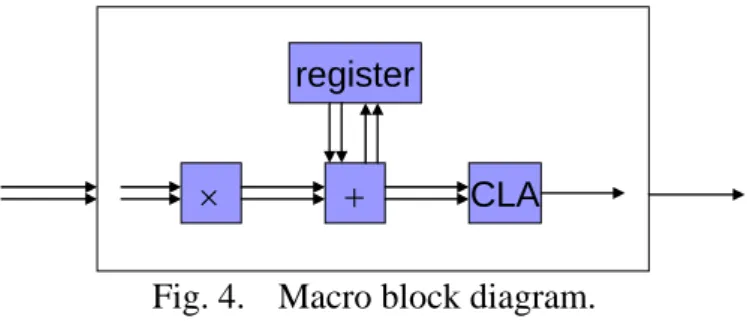
Here first shows a simplest design of floating-point matrix multiplier for presenting our work. This design contains a modular floating-point multiplier, a modular floating-point adder, a register for storing intermediate results and a CLA for final addition. The macro block diagram is shown in Fig. 4. Then the feature of scalable can be described.
register
CLA Fig. 4. Macro block diagram.
In Fig. 4, the arrows between the blocks are dataflow. The outer block represents a MAC which computes accumulation of productions. Thus a sequence of floating-point numbers is inputted to the outer block in order, pair by pair. It outputs result of one inner product. The multiplier block is in charge of generating two-vector partial products of floating-point multiplications. The adder block adds the inputted mantissa vectors up, reduces them into two vectors and outputs them. The register only provides storage space without computational function. The CLA sums up the two inputted vectors into one vector.
Fig. 5 presents a 44 matrix multiplication example for explaining its working processes. The algorithm for computing one entry is shown in Fig. 6. With duplicate designing blocks or repeating its working process, the entire matrix multiplication can be achieved. 44 43 42 41 34 33 32 31 24 23 22 21 14 13 12 11 44 43 42 41 34 33 32 31 24 23 22 21 14 13 12 11 44 43 42 41 34 33 32 31 24 23 22 21 14 13 12 11 C C C C C C C C C C C C C C C C B B B B B B B B B B B B B B B B A A A A A A A A A A A A A A A A
Fig. 5. A 44 matrix multiplication.
Ctemp = 0 //initialization
For k = 1 to 4 Do
Ctemp = Ctemp + Ai,kBk,j
End of k loop
Fig. 6. The algorithm for computation one
Note that i, j and k are the row number and the
column number of Ci,j, and the number of terms in
each inner product, respectively. Ctemp is the
register in Fig. 4. The multiplication and addition arithmetic symbols in Fig. 6 represent the floating-point multiplier and adder blocks in Fig. 4, respectively.
Suppose C1,1 is going to be computed. The
symbol i and j are both one. First, the data in register is initialized to zero. Then it starts to repeat
the loop. The operands of first multiplication, A1,1
and B1,1 are then loaded into the multiplier. Since
the multiplier does not accomplish final two-vector addition, the two vectors are sent to the adder as one of the operands. In other words, each operand of the adder has two-vector partial mantissas. Another operand of the adder is from register. The following step is using CSAs to reducing four vector inputs to two vectors. Significantly, there are two complement bits additionally besides the four vectors. We discuss these complement bits later. After the reduction the adder outputs two vectors and stores back to the register with the exponent. The second multiplication starts while the multiplier can be used, and it repeats the same processes three times in the above. When the last product vectors have been added, the result of addition will be transferred to the CLA block. This block sums up two vectors and gives the final result. Then one result of the matrix C is calculated. No matter how big the size of dimension of the matrix is, this simplest floating-point matrix multiplier could complete the task.
The exponent data flow shown in Fig. 7 is an important issue. First, when the addition operation
is undergoing, the greater exponent between eAB
and eCtemp will be the exponent of the addition
result, noted by e' I1 . However, the addition
operation may result in overflow. If overflow occurs, the exponent should increase by one;
otherwise zero. The increment is denoted by e' I2.
The addition result is the value of Ctemp. Clearly, the
exponent of Ctemp consists of two exponent vectors,
e' I1 and e' I2, and both of them will be stored into
the register. Before the adder adds MAB and Ctemp,
the difference between eAB and eCtemp needs to be
calculated. Here uses eAB to minus eCtemp. The
exponent vectors loaded from the register are eI1
and eI2. Hence, the equation to find the difference d
is demonstrated as (2). d = eA + eB eI1 eI2 (2) 1 I e 2 I e A,B register Difference Computing Exponents of A,B Exponents of Ctemp
Addition Unit Right shift or not ?
No, 0 bias Yes, 1 bias
Fig. 7. The data flow of the exponents. Equation (2) contains three addition operations. If the addition operations are solely implemented by CLA, the difference computation will be on the critical path of the whole design. When the two
vectors of MAB are generated, d is still under
computing. The shifting operation of the adder can not start immediately. To solve this bottleneck, we take advantage of CSA again. Reducing four vectors to two could be resolved by CSA easily. The CLA only is used in the final step. This solution helps the shifting operation can work at
once when the two vectors of MAB are generated.
Thus the delay decreases.
Fig. 8 is the detail block diagram of the simplest design. On the upper left corner is the register
which stores the intermediate result Ctemp and its
two exponent vectors. On the upper right corner section circled by red lines is the proposed multiplier and the other area is the proposed adder. The final two vectors addition CLA block only concerns in the last stage, so that it is not drawn on.
Partial Products Generation Mantissas
Partial Products Reduction (CSA)
Shifter (two vectors) Comparison Block
MAMB
Exponents
eA eB CtempRegister
(two vectors & its exponent)
Intermediate Result
Shifter (two vectors)
if 1’s complement differences
CSA (6 to 2) Leading one (zero) detector
Shifter New Intermediate Result Exponent Computation Parallel Shifter eI1 eI2
Leading one signal
SB SA+ eI1,eI2 eA,eB d11 Complement Bits 0 1 I e eI2
Fig. 8. Block diagram of our design.
The multiplier only generates the partial products and reduces them into two vectors plus a 2’s complement handling operation. Since the mantissa
of MAMB does not have sign but Ctemp has, MAB
must transform to 2’s complement for easy computation. The process of 2’s complement has two steps. First is to transform to 1’s complement. Second is to add one at the least significant bit of
the vector. The addition operation costs lots of time, so we leave it to the reduction stage in the proposed
adder. Notably, MAB has two vectors, so we
directly add one at the second least significant bit.
The output of SASB decides whether it is negative.
While it is one, then the 1’s complement operation will be executed and the complement bit is one. To
summarize the multiplier, it consumes MA and MB,
and outputs a two-vector product plus a complement bit signal.
The register stores the intermediate results
including Ctemp and its two exponent vectors, eI1
and eI2. The proposed adder is in charge of
computing exponents and addition of two two-vector inputs.
B. Comparison block
The adder and multiplier can process in parallel. When the two floating-point is loaded into this simple design, the comparison block starts to calculate the difference since it only needs the exponents. In Fig. 9, the calculation for
eA+eBeI1eI2 is to append each vector a sign bit,
then to make eI1 and eI2 1’s complement. The four
vectors will be reduced by CSA. This reduction uses a trick that the least significant column is reduced to one bit. This can be done at the second reduction stage by using a FA at the least significant column since there is no carry from lower column. As a result, when the four vectors are reduced, there is only one bit at the least significant column. Two ones are then filled into the last column to accomplish the 2’s complement
transformations of eI1 and eI2. The least significant
bit of the addition CLA can be implemented by a FA, thus three bits at the least significant column can be added.
Difference = eAeBeI1eI2
… … … … … … … … … … … 1 12-bit CLA Cin 1 1 Bit 11 0 0 Bit 11 Bit 11 1 Sign Stage 1 Stage 2 FA eA eB eI1 eI2
Fig. 9. An illustration for computing the
difference.
In Fig. 10, this comparison block would send
two differences to the parallel shifter, one for Ctemp
and another for MAB. There is always at least one
difference is zero cause we use the sign of the
difference, denoted by d11, to do the AND logic.
The difference is sent directly to the shifter for
Ctemp, and the inverted difference is sent to MAB
shifter. On the other hands, this comparison block
also sends the greater group, eA+eB or eI1+eI2, to the
exponent computation block according to the sign bit of the difference.
12-bit CLA Reduce 4 to 2 vectors Cin=1 d0~d10 d11 d0~d10 (d0~d10) AND
AND Shift amount for MAMB
Shift amount for IR
Greater exponent
eI1,eI2 eA,eB d11
Fig. 10. Dispatching the difference. C. Parallel shifters
As the MAB arrives, the Ctemp and differences are
all ready. The parallel shifters start immediately. The shifters are implemented based on multiplexers. Each bit of the difference controls a level of shifter.
The bit b controls one time 2b-bit shift, where b is
the bit number. The difference has 11 bits. Since the length of the inputs is not more than 107 bits, only bits 0 to 6 of the difference are needed to control the right shifts. If any one of the bits after 7 is not zero, the right shifts must more than 127 bits, then these bits are combined to pull down the data to zero. Each stage of right shift for each bit is implemented by a 2 to 1 multiplexer. The parallel shifters’ illustrations are shown in Fig. 11. Since the
MAB shifter receives the inverted difference, we
must shift one more bit to complete the 2’s
complement. Thus the shifter for MAB has some
different at shift stage seven. The d11 is used to
control if shifts one more bit.
Bit 6 … … Bit 5 … … Bit 1 … … … … … OR OR Bit 10 Bit 9 Bit 8 Bit 7 NOR … AND … Bit 0 Carry and sum vectors
Multiplexer-Based Barrel Shifter for MAMB
difference
…
d11
D. CSA block
This block mainly reduces the four shifted vectors to two. Due to the 2’s complement representation transformation, the four shifted vectors should plus two complement bits at the second least significant column. Thus there are four bits in each column except the second least significant column has six. Since this proposed adder is designed for modularization, it also can connect to two proposed multipliers. Therefore the complement bits are two. However, in this modularized design, the intermediate results in register are already in 2’s complement representation. One of the complement bit is always zero, and another one depends on the signal transmitted by the forward multiplier. Nonetheless, no matter the number of uncertain complement bits is, the number of reduction stages is three.
E. Normalization
This process includes two blocks, one is leading one (zero) detector, and another one is a shifter which right shifts one bit or zero. The detector checks two vectors whether any one of them overflows. While the overflow occurs, both of them right shift one bit and the detector sends one bit signal to the exponent computation block. The signal is called NS signal. One represents there has no shift; otherwise the two vectors right shift. F. Exponent computation
This block receives the two exponents of the greater exponent group from the comparison block,
V1 and V2, which are eA and eB or eI1 and eI2.Then it
computes V1+V21023 as new eI1 denoted by e' I1. It
also receives the NS signal to computes the new eI2
denoted by e' I2. Because e' I2 just has two different
values like NS does, it is very easy to computes e' I2
by only a simple logic layout.
The above example in Fig. 5 is resolved by a simplest design. When a developer has more demand on less delay, there are other ways to implement a faster floating-point matrix multiplier. It is shown in Fig. 12. + + register CLA
Fig. 12. The design consuming two pairs of
multiplications.
The design in Fig. 12 uses two multipliers, two
adders, one register and a final addition CLA. It can multiply two pairs of floating-point numbers at one time, so that the four multiplications and accumulations of one element computation could be done in two steps. Then repeat these computation 16 times, the whole matrix multiplication is done. The third design in Fig. 13 is that uses four multipliers, three adders and a final addition CLA. Apparently it can resolve one element in one step. If the demand is the fastest speed, just duplicate this design 16 times. Each copy computes a specific element of the matrix. Thus a very high speed is gained.
+ + CLA +
Fig. 13. The design consuming four pairs of
multiplications.
IV. COMPARISONS
To estimate our design, a widely accepted approach is described in the following. This method takes any monotonic gate (e.g. AND, NOR, etc.) has one gate delay and cost excluding the XOR gate which has two gate delays and costs.
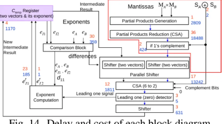
Fig. 14 reveals the delay and cost of each block in our simplest design. The delay and cost of each
block are shown by its side. Since e' I1 and e' I2 are
computed in different processes, the delay and cost are described separately. The critical path of this design is from partial products generation block to overflow shifter block. Totally the sum of delay through this path is 74 and cost of whole diagram is 39127.
Partial Products Generation Mantissas
Partial Products Reduction (CSA)
Shifter (two vectors) Comparison Block
MAMB
Exponents
eA eB CtempRegister
(two vectors & its exponent)
Intermediate Result
Shifter (two vectors)
if 1’s complement differences
CSA (6 to 2) Leading one (zero) detector
Shifter New Intermediate Result Exponent Computation Parallel Shifter eI1 eI2
Leading one signal
SB SA+ eI1,eI2 eA,eB d11 Complement Bits 0 1 2809 36 18488 17 13242 12 2 424 1811 2 2 3 5 3 631 30 359 4 1170 1 1 23 185 1 I e eI2
Fig. 14. Delay and cost of each block diagram. We separate a floating-point matrix multiplier
into four parts, the multiplier, the adder, the register, and the final addition CLA. Then compare these units with those in [4]. Note that in [4], there is no final addition CLA, because both of multiplier and adder in Bensaali’s have a CLA. The rounding process is skipped in both works. Since rounding is after the CLA addition, skipping rounding makes Bensaali’s work better. On the other hands, there is only one CLA in the final addition in our work, so that rounding speed has no noticeable effect.
Table 1 is the delay and cost of each unit of a matrix multiplier for our and Bensaali’s work. The major difference between ours and Bensaali’s is that the proposed design has a CLA for final addition while Bensaali’s has one CLA in each multiplier and adder so that our multiplier and adder have shorter delay than Bensaali’s.
Table 1 Delay and Cost of Each Component Unit.
Ours Bensaali et al. Delay Cost Delay Cost Multiplication Unit 39 21723 71 22488
Addition Unit 35 16234 79 8734
Register 4 1170 4 320
CLA (Final Addition) 32 767
The comparison is under three different designs. All of these designs are used to resolve one element of an 88 matrix multiplication. The three designs are drawn in Fig. 15, Fig. 16 and Fig. 17. They have different delay and cost. The first one is the simplest design as the above example. The second has 8 multipliers and 7 adders plus a final addition CLA. It makes an effort to accomplish the computation as fast as possible. The last one attempts to find the balance between delay and cost with 4 multipliers, 4 adders, 1 register and a final addition CLA. The comparing result is showed in Table 2.
Fig. 15. The first comparison.
Table 2 Comparison with Bensaali’s under the
Three Structures.
Ours Bensaali et al. Delay Cost DelayCost Delay Cost DelayCost First 379 39,894 15,119,826 731 31,542 23,057,202 Second 236 288,189 68,012,604 308 241,042 74,240,936 Third 275 153,765 42,285,375 391 125,208 48,956,328
Fig. 16. The second comparison.
Fig. 17. The third comparison
Apparently, in these three designs, our costs are higher than Bensaali’s as shown in Table 3. The main reason is that we always reserve two vectors in the intermediate processes. Since shift operation could not be avoided, shifting two vectors spends more cost. Nonetheless, each delay (delay cost) in three designs are decreased. For both of ours and Bensaali’s, the first design uses less cost and highest delay. The fastest speed could be achieved by second design with mass cost.
In the following, Table 3 is the improvement of our work comparing with Bensaali’s.
Table 3 Improvement Compared with Bensaali’s.
Improvement (%)
Delay Cost DelayCost
First 48.2 26.5 34.4
Second 23.4 19.6 8.4
Third 29.7 22.8 13.6
The result shows that with cost increasing 19%~ 26%, the computation time could improve 23%~48%. In the first design, our work gains the most desirable improvement. Although the cost increases, we still achieve higher performance and better delay cost.
V. CONCLUSION
Floating-point matrix multiplication is widely used in several scientific computations. In general,
a parallel processing architecture is often adopted for speeding up the matrix multiplication. Many efforts are done to achieve high performance or implement on FPGAs. This work proposes a design of floating-point matrix multiplier. The delay of the multiply unit and addition unit in this work are 39 and 35, respectively. In contrast, those in Bensaali’s are 71 and 79. Thus the delay improvement in the multiply unit and addition unit are 45.1% and 55.7%. In the simplest design of a floating-point matrix multiplier, the delay and delaycost improve 48.2% and 34.4%, respectively. As a result, eliminating the usage of CLA in the critical path except the final addition makes a floating-point matrix multiplier perform better. The multiplier and adder of the floating-point matrix multiplier are modular so that the matrix multiplier is scalable by arranging them with duplicate modules. Complex combinations lead to cost increasing but less delay. Depending on the demands of delay and cost, users can decide an optimized design of a floating-point matrix multiplier by evaluating carefully. The speed improved by using CSA to sum up the intermediate result. However, the cost lightly increases. The future work is to reduce the cost to achieve a more efficient design of a floating-point matrix multiplier.
ACKNOWLEDGMENT
The authors would like to thank the National Science Council of the Republic of China, Taiwan for financially supporting this research under Contract No. NSC-97-2221-E-260-001-.
REFERENCE
[1] ANSI/IEEE Standard 754-1985: IEEE Standard for Binary Floating-Point Arithmetic. Piscataway, NJ: IEEE Press, 1985.
[2] A. Beaumont-Smith, N. Burgess, S. Lefrere, and C. Lim, “Reduced latency IEEE floating-point standard adder architectures,” Proc. 14th IEEE Symp. Computer Arithmetic, pp. 35-43, 1999.
[3] F. Bensaali, A. Amira, and A. Bouridane, “Accelerating matrix product on reconfigurable hardware for image processing applications,” IEE Proceedings of Circuits, Devices and Systems, vol. 152, no. 3, pp. 236-246, 2005.
[4] F. Bensaali, A. Amira, and R. Sotudeh, “Floating-point matrix product on FPGA,” ACS/IEEE International Conference on Computer Systems and Applications
(AICCSA'7), pp. 466-473, 2007.
[5] G. Choe and E.E. Swartzlander, Jr., “Merged Arithmetic for computing wavelet transforms,” in Proceedings of the 8th Great Lakes Symposium on VLSI, pp. 196-201, 1998.
[6] Y. Dou, S. Vassiliadis, G. K. Kuzmanov, and G.N. Gaydadjiev, “64-bit floating-point FPGA matrix multiplication,” Proc.2005 ACM/SIGDA 13th Int. Symp. on FPGA, pp. 86–95, 2005.
[7] H.A.H. Fahmy, A.A. Liddicoat and M. J. Flynn, “Improving the effectiveness of floating point arithmetic,” 35th Asiloma Conference on Signals, Systems and Computers, Vol 1, pp 875-879, November 2001.
[8] K.A. Feiste and E.E. Swatzlander, Jr., “Merged arithmetic revisited,” in Proceedings of the IEEE Workshop on Signal Processing Systems, 1997, pp. 212-221.
[9] H.P. Huang and D.R. Duh, “Fast computation algorithm for robot dynamics and its implementation,” in Proceedings of the IEEE International Symposium on Industrial Electronics, 1992, pp. 352-356.
[10] J.W. Jang, S.B. Choi, and V.K. Prasanna, “Energy- and time-efficient matrix multiplication on FPGAs,” IEEE Transaction on Very Large Scale Integration Systems, vol. 13, no. 11, pp. 1305-1319, November 2005. [11] G. Kuzmanov and W.M. van Oijen,
“Floating-point matrix multiplication in a polymorphic processor,” International Conference on Field-Programmable Technology (ICFPT ), pp. 249-252, December 2007.
[12] W.C. Park, T.D. Han, and S.D. Kim, “Efficient simultaneous rouding method removing sticky-bit from critical path for floating point addition,” The Second IEEE Asia Pacific Conference on ASICs, pp. 223-226, August 2000.
[13] W.C. Park, S.W. Lee, O.Y. Kwon, T.D. Han, and S.D. Kim, "Floating-point adder/subtractor performing IEEE rounding and addition/subtraction in parallel," IEICE Trans. Information and Systems, vol. 4, pp. 297-305, 1996
[14] N.T. Quach, N. Takagi, and M.J. Flynn, “Systematic IEEE rounding method for high-speed floating-point multipliers,” IEEE
Transactions on Very Large Scale Integration (VLSI) Systems, vol. 12, no. 5, May 2004. [15] P.M. Seidel and G. Even, “Delay-optimized
implementation of IEEE floating-point addition,” IEEE Transaction On Computers, vol. 53, no. 2, pp. 97-113, February 2004. [16] V. Strassen, “Gaussian elimination is not
optimal,” Number. Math., vol.13, pp. 354-356, 1969.
[17] E.E. Swartzlander, Jr., “Merged arithmetic,” IEEE Transaction on Computers, vol. C-29, no. 10, pp. 946-950, October 1980.
[18] L. Zhuo and V.K. Prasanna, “Scalable and modular algorithms for floating-point matrix multiplication on FPGAs,” in Proceedings of the 18th International Parallel and Distributed Processing Symposium (IPDPS’4), pp. 94-103, 2004.
[19] L. Zhuo and V.K. Prasanna, “Scalable and modular algorithms for floating-point matrix multiplication on reconfigurable computing systems,” IEEE Trans. Parallel and Distributed Systems, vol. 18, no. 4, pp. 433–448, 2007.